

Page 1
Stereo Audio, 24-Bit,
a
FEATURES
5.0 V Stereo Audio ADC
with 3.3 V Tolerant Digital Interface
Supports 96 kHz Sample Rates
Supports 16-/20-/24-Bit Word Lengths
Multibit Sigma-Delta Modulators with
“Perfect Differential Linearity Restoration” for
Reduced Idle Tones and Noise Floor
105 dB (Typ) Dynamic Range
Supports 256/512 and 768 ⴛ f
Flexible Serial Data Port
Allows Right-Justified, Left-Justified, I
and DSP Serial Port Modes
Cascadable (up to Four Devices) from a Single DSP
SPORT
Device Control via SPI Compatible Serial Port or
Optional Control Pins
On-Chip Reference
28-Lead SSOP Package
APPLICATIONS
Professional Audio
Mixing Consoles
Musical Instruments
Digital Audio Recorders, Including
CD-R, MD, DVD-R, DAT, HDD
Home Theater Systems
Automotive Audio Systems
Multimedia
Master Clocks
S
2
S Compatible
96 kHz, Multibit ⌺-⌬ ADC
AD1871
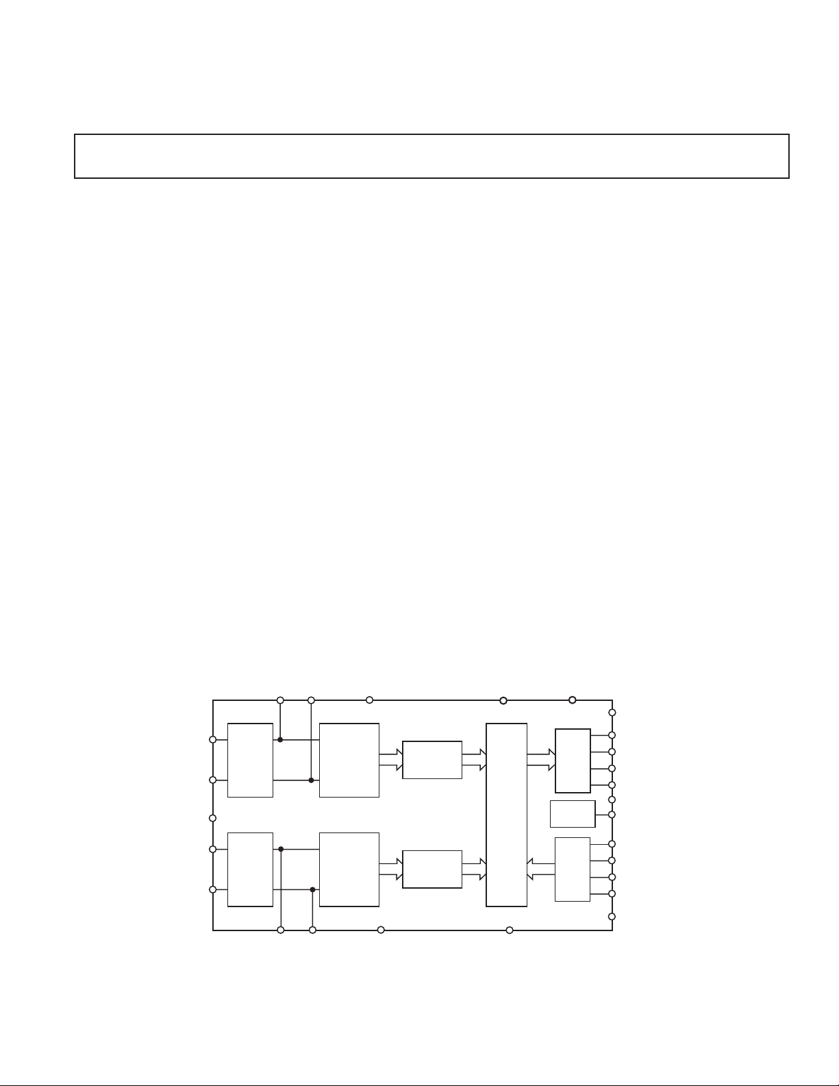
PRODUCT OVERVIEW
The AD1871 is a stereo audio ADC intended for digital audio
applications requiring high performance analog-to-digital
conversion. It features two 24-bit conversion channels each
with programmable gain amplifier (PGA), multibit sigma-delta
modulator, and decimation filters. Each channel provides 105 db
of dynamic range, making the AD1871 suitable for applications
such as digital audio recorders and mixing consoles.
Each of the AD1871’s input channels (left and right) can be
configured as either differential or single-ended (two inputs
muxed with internal single-ended-to-differential conversion).
The input PGA features a gain range of 0 dB to 12 dB in steps
of 3 dB. The Σ-∆ modulator features a proprietary multibit
architecture that realizes optimum performance over an audio
bandwidth with standard audio sampling rates of 32 kHz up to
96 kHz. The decimation filter response features very low passband ripple and excellent stop-band attenuation.
The AD1871’s audio data interface supports all common interface
formats such as I
modes that allow for convenient connection to general-purpose
digital signal processors (DSPs). The AD1871 also features an
SPI compatible serial control port that allows for convenient
control of device parameters and functionality such as sample
word-width, PGA settings, interface modes, and so on.
The AD1871 operates from a single 5 V power supply—with
an optional digital interfacing capability of 3.3 V. It is housed in
a 28-lead SSOP package and is characterized for operation
over the temperature range –40°C to +105°C.
2
S, left-justified, right-justified as well as other
FUNCTIONAL BLOCK DIAGRAM
CAPLN CAPLP AVDD DVDD ODVDD
VINLP
VINLN
VREF
VINRP
VINRN
ANALOG
INPU T
BUFFER
ANALOG
INPU T
BUFFER
CAPRN CAPRP AGND DGND
MULTIBIT
⌺-⌬
MODULATOR
MULTIBIT
⌺-⌬
MODULATOR
AD1871
REV. 0
Information furnished by Analog Devices is believed to be accurate and
reliable. However, no responsibility is assumed by Analog Devices for its
use, nor for any infringements of patents or other rights of third parties that
may result from its use. No license is granted by implication or otherwise
under any patent or patent rights of Analog Devices.
CASC
LRCLK
DECIMATOR
FILTER
ENGINE
DECIMATOR
One Technology Way, P.O. Box 9106, Norwood, MA 02062-9106, U.S.A.
Tel: 781/329-4700 www.analog.com
Fax: 781/326-8703 © Analog Devices, Inc., 2002
DATA
PORT
CLOCK
DIVIDER
SPI
PORT
BCLK
DOUT
DIN
RESET
MCLK
CLATCH/(M/S)
CCLK/(256/512)
CIN/(DF1)
COUT/(DF0)
XCTRL
Page 2

AD1871
TABLE OF CONTENTS
FEATURES . . . . . . . . . . . . . . . . . . . . . . . . . . . . . . . . . . . . . . . . . . . . . . . . . . . . . . . . . . . . . . . . . . . . . . . . . . . . . . . . . . . . . . . . . . . 1
FUNCTIONAL BLOCK DIAGRAM . . . . . . . . . . . . . . . . . . . . . . . . . . . . . . . . . . . . . . . . . . . . . . . . . . . . . . . . . . . . . . . . . . . . . . . 1
PRODUCT OVERVIEW . . . . . . . . . . . . . . . . . . . . . . . . . . . . . . . . . . . . . . . . . . . . . . . . . . . . . . . . . . . . . . . . . . . . . . . . . . . . . . . . . 1
SPECIFICATIONS . . . . . . . . . . . . . . . . . . . . . . . . . . . . . . . . . . . . . . . . . . . . . . . . . . . . . . . . . . . . . . . . . . . . . . . . . . . . . . . . . . . . . 3
TEST CONDITIONS UNLESS OTHERWISE SPECIFIED . . . . . . . . . . . . . . . . . . . . . . . . . . . . . . . . . . . . . . . . . . . . . . . . . . . . . 3
ANALOG PERFORMANCE . . . . . . . . . . . . . . . . . . . . . . . . . . . . . . . . . . . . . . . . . . . . . . . . . . . . . . . . . . . . . . . . . . . . . . . . . . . . . . 3
LOW-PASS DIGITAL FILTER CHARACTERISTICS . . . . . . . . . . . . . . . . . . . . . . . . . . . . . . . . . . . . . . . . . . . . . . . . . . . . . . . . . 4
HIGH-PASS DIGITAL FILTER CHARACTERISTICS . . . . . . . . . . . . . . . . . . . . . . . . . . . . . . . . . . . . . . . . . . . . . . . . . . . . . . . . 4
MASTER CLOCK (MCLK) AND RESET TIMING . . . . . . . . . . . . . . . . . . . . . . . . . . . . . . . . . . . . . . . . . . . . . . . . . . . . . . . . . . . 4
DATA INTERFACE TIMING . . . . . . . . . . . . . . . . . . . . . . . . . . . . . . . . . . . . . . . . . . . . . . . . . . . . . . . . . . . . . . . . . . . . . . . . . . . . 5
CONTROL INTERFACE TIMING . . . . . . . . . . . . . . . . . . . . . . . . . . . . . . . . . . . . . . . . . . . . . . . . . . . . . . . . . . . . . . . . . . . . . . . . 8
DIGITAL I/O . . . . . . . . . . . . . . . . . . . . . . . . . . . . . . . . . . . . . . . . . . . . . . . . . . . . . . . . . . . . . . . . . . . . . . . . . . . . . . . . . . . . . . . . . . 8
POWER . . . . . . . . . . . . . . . . . . . . . . . . . . . . . . . . . . . . . . . . . . . . . . . . . . . . . . . . . . . . . . . . . . . . . . . . . . . . . . . . . . . . . . . . . . . . . . 8
TEMPERATURE RANGE . . . . . . . . . . . . . . . . . . . . . . . . . . . . . . . . . . . . . . . . . . . . . . . . . . . . . . . . . . . . . . . . . . . . . . . . . . . . . . . . 8
ABSOLUTE MAXIMUM RATINGS . . . . . . . . . . . . . . . . . . . . . . . . . . . . . . . . . . . . . . . . . . . . . . . . . . . . . . . . . . . . . . . . . . . . . . . 9
ORDERING GUIDE . . . . . . . . . . . . . . . . . . . . . . . . . . . . . . . . . . . . . . . . . . . . . . . . . . . . . . . . . . . . . . . . . . . . . . . . . . . . . . . . . . . . 9
PIN CONFIGURATION . . . . . . . . . . . . . . . . . . . . . . . . . . . . . . . . . . . . . . . . . . . . . . . . . . . . . . . . . . . . . . . . . . . . . . . . . . . . . . . . . 9
PIN FUNCTION DESCRIPTIONS . . . . . . . . . . . . . . . . . . . . . . . . . . . . . . . . . . . . . . . . . . . . . . . . . . . . . . . . . . . . . . . . . . . . . . . 10
TERMINOLOGY . . . . . . . . . . . . . . . . . . . . . . . . . . . . . . . . . . . . . . . . . . . . . . . . . . . . . . . . . . . . . . . . . . . . . . . . . . . . . . . . . . . . . . 12
TYPICAL PERFORMANCE CURVES . . . . . . . . . . . . . . . . . . . . . . . . . . . . . . . . . . . . . . . . . . . . . . . . . . . . . . . . . . . . . . . . . . . . . 13
Filter Responses . . . . . . . . . . . . . . . . . . . . . . . . . . . . . . . . . . . . . . . . . . . . . . . . . . . . . . . . . . . . . . . . . . . . . . . . . . . . . . . . . . . . . 13
Device Performance Curves . . . . . . . . . . . . . . . . . . . . . . . . . . . . . . . . . . . . . . . . . . . . . . . . . . . . . . . . . . . . . . . . . . . . . . . . . . . . 14
FUNCTIONAL DESCRIPTION . . . . . . . . . . . . . . . . . . . . . . . . . . . . . . . . . . . . . . . . . . . . . . . . . . . . . . . . . . . . . . . . . . . . . . . . . . 16
Clocking Scheme . . . . . . . . . . . . . . . . . . . . . . . . . . . . . . . . . . . . . . . . . . . . . . . . . . . . . . . . . . . . . . . . . . . . . . . . . . . . . . . . . . . . 16
Modulator . . . . . . . . . . . . . . . . . . . . . . . . . . . . . . . . . . . . . . . . . . . . . . . . . . . . . . . . . . . . . . . . . . . . . . . . . . . . . . . . . . . . . . . . . . 16
Digital Decimating Filters . . . . . . . . . . . . . . . . . . . . . . . . . . . . . . . . . . . . . . . . . . . . . . . . . . . . . . . . . . . . . . . . . . . . . . . . . . . . . . 17
High-Pass Filter . . . . . . . . . . . . . . . . . . . . . . . . . . . . . . . . . . . . . . . . . . . . . . . . . . . . . . . . . . . . . . . . . . . . . . . . . . . . . . . . . . . . . 17
ADC Coding . . . . . . . . . . . . . . . . . . . . . . . . . . . . . . . . . . . . . . . . . . . . . . . . . . . . . . . . . . . . . . . . . . . . . . . . . . . . . . . . . . . . . . . . 17
Analog Input Section . . . . . . . . . . . . . . . . . . . . . . . . . . . . . . . . . . . . . . . . . . . . . . . . . . . . . . . . . . . . . . . . . . . . . . . . . . . . . . . . . 17
Serial Data Interface . . . . . . . . . . . . . . . . . . . . . . . . . . . . . . . . . . . . . . . . . . . . . . . . . . . . . . . . . . . . . . . . . . . . . . . . . . . . . . . . . . 17
CONTROL/STATUS REGISTERS . . . . . . . . . . . . . . . . . . . . . . . . . . . . . . . . . . . . . . . . . . . . . . . . . . . . . . . . . . . . . . . . . . . . . . . . 20
Control Register I . . . . . . . . . . . . . . . . . . . . . . . . . . . . . . . . . . . . . . . . . . . . . . . . . . . . . . . . . . . . . . . . . . . . . . . . . . . . . . . . . . . . 21
Control Register II . . . . . . . . . . . . . . . . . . . . . . . . . . . . . . . . . . . . . . . . . . . . . . . . . . . . . . . . . . . . . . . . . . . . . . . . . . . . . . . . . . . 22
Control Register III . . . . . . . . . . . . . . . . . . . . . . . . . . . . . . . . . . . . . . . . . . . . . . . . . . . . . . . . . . . . . . . . . . . . . . . . . . . . . . . . . . . 23
Peak Reading Registers . . . . . . . . . . . . . . . . . . . . . . . . . . . . . . . . . . . . . . . . . . . . . . . . . . . . . . . . . . . . . . . . . . . . . . . . . . . . . . . . 24
EXTERNAL CONTROL . . . . . . . . . . . . . . . . . . . . . . . . . . . . . . . . . . . . . . . . . . . . . . . . . . . . . . . . . . . . . . . . . . . . . . . . . . . . . . . . 24
Master/Slave Select . . . . . . . . . . . . . . . . . . . . . . . . . . . . . . . . . . . . . . . . . . . . . . . . . . . . . . . . . . . . . . . . . . . . . . . . . . . . . . . . . . . 24
MCLK Mode Select . . . . . . . . . . . . . . . . . . . . . . . . . . . . . . . . . . . . . . . . . . . . . . . . . . . . . . . . . . . . . . . . . . . . . . . . . . . . . . . . . . 24
Serial Data Format Select . . . . . . . . . . . . . . . . . . . . . . . . . . . . . . . . . . . . . . . . . . . . . . . . . . . . . . . . . . . . . . . . . . . . . . . . . . . . . . 24
MODULATOR MODE . . . . . . . . . . . . . . . . . . . . . . . . . . . . . . . . . . . . . . . . . . . . . . . . . . . . . . . . . . . . . . . . . . . . . . . . . . . . . . . . . 24
INTERFACING . . . . . . . . . . . . . . . . . . . . . . . . . . . . . . . . . . . . . . . . . . . . . . . . . . . . . . . . . . . . . . . . . . . . . . . . . . . . . . . . . . . . . . . 25
Analog Interfacing . . . . . . . . . . . . . . . . . . . . . . . . . . . . . . . . . . . . . . . . . . . . . . . . . . . . . . . . . . . . . . . . . . . . . . . . . . . . . . . . . . . 25
LAYOUT CONSIDERATIONS . . . . . . . . . . . . . . . . . . . . . . . . . . . . . . . . . . . . . . . . . . . . . . . . . . . . . . . . . . . . . . . . . . . . . . . . . . 26
OUTLINE DIMENSIONS . . . . . . . . . . . . . . . . . . . . . . . . . . . . . . . . . . . . . . . . . . . . . . . . . . . . . . . . . . . . . . . . . . . . . . . . . . . . . . . 27
–2–
REV. 0
Page 3

AD1871–SPECIFICA TIONS
TEST CONDITIONS UNLESS OTHERWISE NOTED
Supply Voltages . . . . . . . . . . . . . . . . . . . . . . 5.0 V
Ambient Temperature . . . . . . . . . . . . . . . . . 25∞C
Input Clock (f
Input Signal . . . . . . . . . . . . . . . . . . . . . . . . . 991.768 Hz
. . . . . . . . . . . . . . . . . . . . . . . . . . . . . . . . . . –0.5 dB Full Scale (dBFS) (Differential, PGA/MUX Enabled)
Measurement Bandwidth . . . . . . . . . . . . . . . 23.2 Hz to 19.998 kHz
Word Width . . . . . . . . . . . . . . . . . . . . . . . . . 24 Bits
Load Capacitance on Digital Outputs . . . . . 100 pF
Input Voltage High (V
Input Voltage Low (V
Master Mode, Data I
ANALOG PERFORMANCE
Parameter Min Typ Max Unit Conditions
RESOLUTION 24 Bits
DIFFERENTIAL INPUT PGA/MUX Enabled
Dynamic Range (20 Hz to 20 kHz, –60 dB Input)
Unweighted 98 103 dB
A-Weighted 100 105 dB
Signal-to-Noise Ratio 106 dB
Total Harmonic Distortion + Noise –85 dB Input = –0.5 dBFS
(THD+N) –103 dB Input = –20 dBFS
Multibit Modulator Only Modulator Output @ 5.6448 MHz
Dynamic Range (A-Weighted) 102 dB
SINGLE-ENDED INPUT PGA/MUX Enabled
Dynamic Range (20 Hz to 20 kHz, –60 dB Input)
Unweighted 103 dB
A-Weighted 105 dB
Signal-to-Noise Ratio 106 dB
Total Harmonic Distortion + Noise –85 dB Input = –0.5 dBFS
(THD+N) –103 dB Input = –20 dBFS
DIFFERENTIAL INPUT (BYPASS) PGA/MUX Disabled
Dynamic Range (20 Hz to 20 kHz, –60 dB Input)
Unweighted 103 dB
A-Weighted 106 dB
Signal-to-Noise Ratio 106 dB
Total Harmonic Distortion + Noise –86 dB Input = –0.5 dBFS
(THD+N) –104 dB Input = –20 dBFS
DIFFERENTIAL INPUT (f
Dynamic Range (20 Hz to 20 kHz, –60 dB Input)
Unweighted 103 dB
A-Weighted 106 dB
Signal-to-Noise Ratio 106 dB
Total Harmonic Distortion + Noise –87 dB Input = –0.5 dBFS
(THD+N) –104 dB Input = –20 dBFS
Analog Inputs
Differential Input Range (± Full Scale) –2.828 +2.828 V
Input Impedance (PGA/MUX) 8 kW Differential
Input Impedance (ByPass) 40 kW Differential
Input Impedance (PGA/MUX) 4 kW Single Ended
V
REF
DC Accuracy
Gain Error –10 %
Interchannel Gain Mismatch –0.2 –0.01 +0.2 dB
Gain Drift 100 ppm/∞C
Crosstalk (EIAJ Method) –100 dB
) [256 ¥ fS] . . . . . . . . . . 12.288 MHz
CLKIN
) . . . . . . . . . . . . . . . 2.4 V
IH
) . . . . . . . . . . . . . . . 0.8 V
IL
2
S Justified
= 96 kHz) PGA/MUX Enabled; AMC = 1
S
2.138 2.25 2.363 V
REV. 0
–3–
Page 4
AD1871–SPECIFICA TIONS
LOW-PASS DIGITAL FILTER CHARACTERISTICS (fS = 48 kHz)
Parameter Min Typ Max Unit
Decimation Factor 128
Pass-Band Frequency 21.77 kHz
Stop-Band Frequency 26.23 kHz
Pass-Band Ripple ± 0.01 dB
Stop-Band Attenuation 120 dB
Group Delay 910 ms
LOW-PASS DIGITAL FILTER CHARACTERISTICS (fS = 96 kHz)
Parameter Min Typ Max Unit
Decimation Factor 64
Pass-Band Frequency 43.54 kHz
Stop-Band Frequency 52.46 kHz
Pass-Band Ripple ± 0.01 dB
Stop-Band Attenuation 120 dB
Group Delay 460 ms
HIGH-PASS DIGITAL FILTER CHARACTERISTICS (fS = 48 kHz)
Parameter Min Typ Max Unit
Cutoff Frequency 2 Hz
HIGH-PASS DIGITAL FILTER CHARACTERISTICS (fS = 96 kHz)
Parameter Min Typ Max Unit
Cutoff Frequency 4 Hz
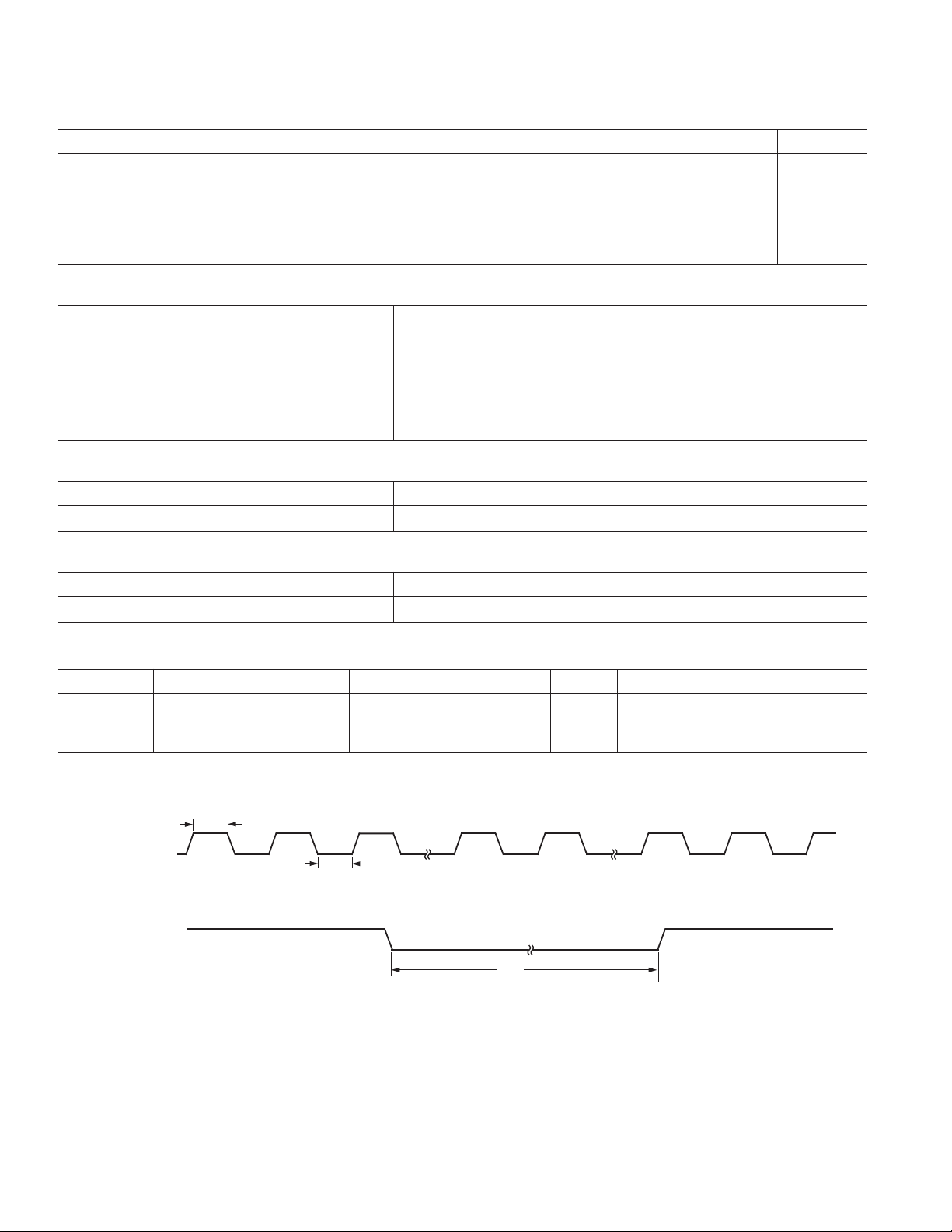
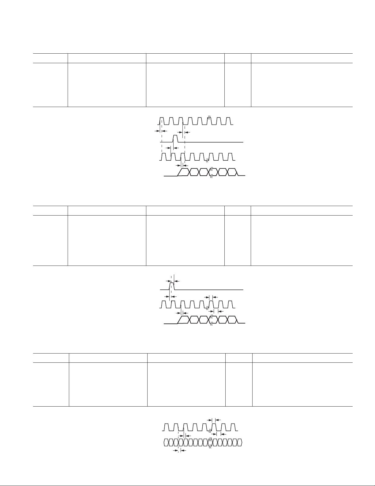
MASTER CLOCK (MCLK) AND RESET TIMING
Mnemonic Description Min Typ Max Unit Comment
t
MCH
t
MCL
t
PDR
MCLK High Width 20 ns
MCLK Low Width 20 ns
RESET Low Pulsewidth 20 ns
t
MCH
MCLK
t
MCL
RESET
t
Figure 1. MCLK/
RESET
PDR
Timing
–4–
REV. 0
Page 5
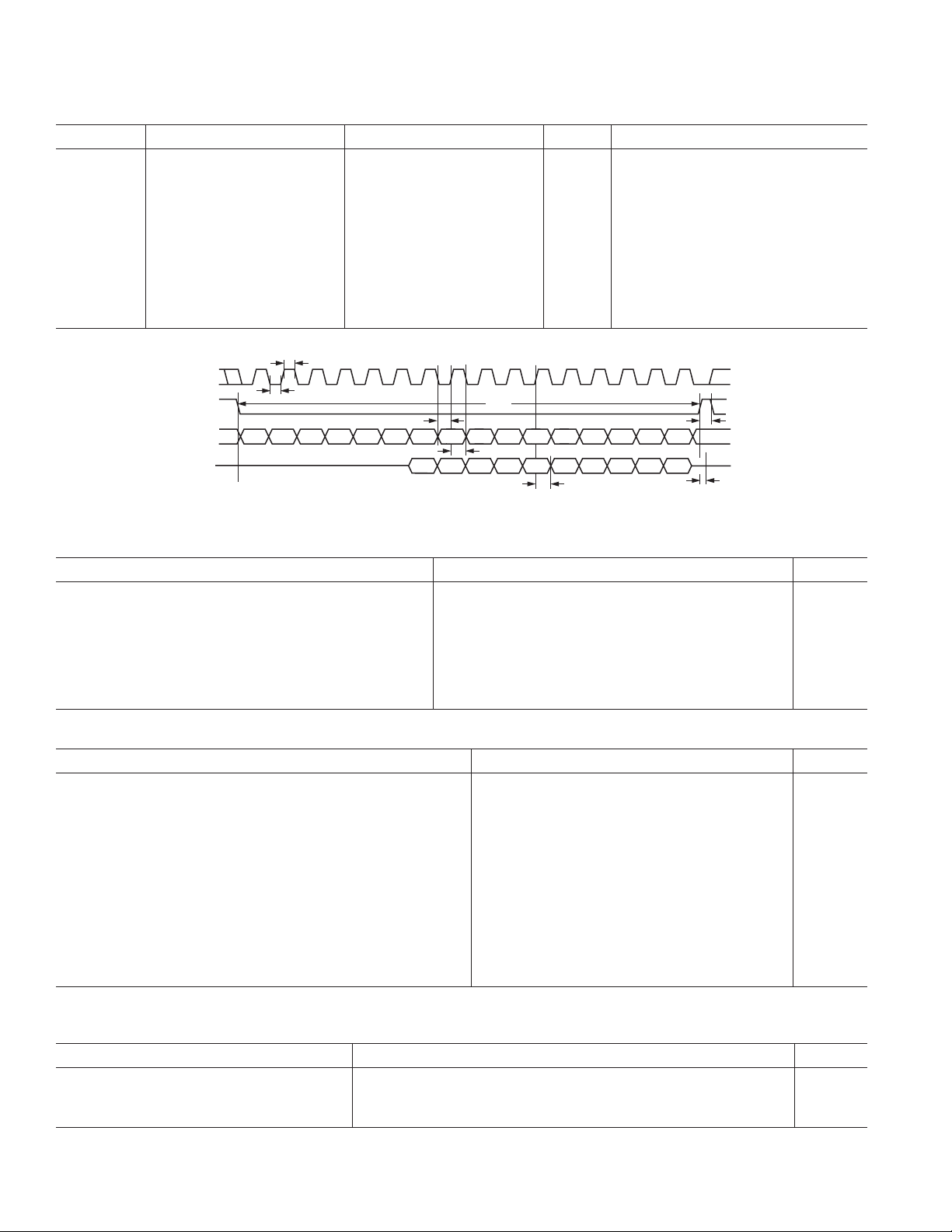
DATA INTERFACE TIMING (STANDALONE MODE–MASTER)
Mnemonic Description Min Typ Max Unit Comment
t
BDLY
t
BLDLY
t
BDDLY
LEFT-JUSTIFIED
2
I
S-JUSTIFIED
BCLK Delay 20 ns From MCLK Rising
LRCLK Delay to Low 10 ns From BCLK Falling
DOUT Delay 10 ns From BCLK Falling
MCLK
t
BDLY
BCLK
t
BLDLY
LRCLK
t
BDDLY
DOUT
MODE
DOUT
MODE
MSB
MSB–
MSB
1
AD1871
RIGHT-JUSTIFIED
DOUT
MODE
8-BIT CLOCKS
(24-BIT DATA)
12-BIT CLOCKS
(20-BIT DATA)
16-BIT CLOCKS
(16-BIT DATA)
MSB
Figure 2. Master Data Interface Timing
LSB
REV. 0
–5–
Page 6
AD1871
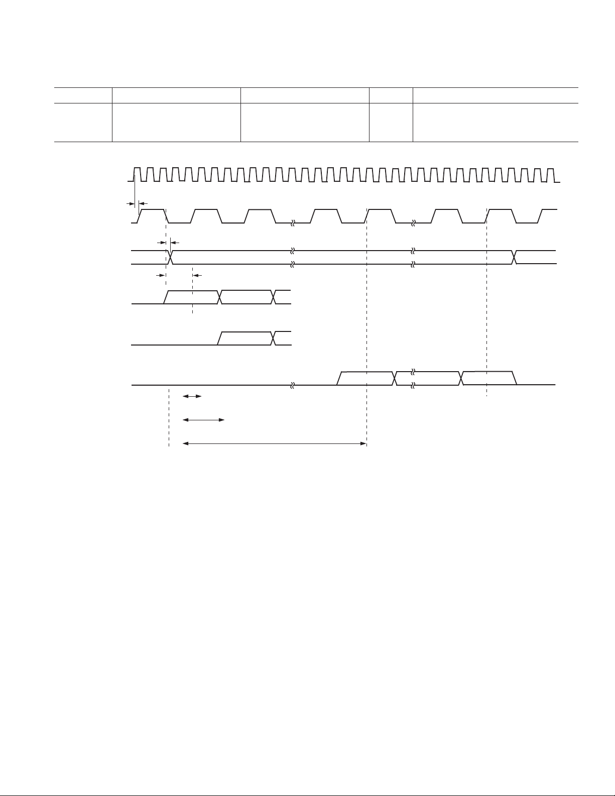
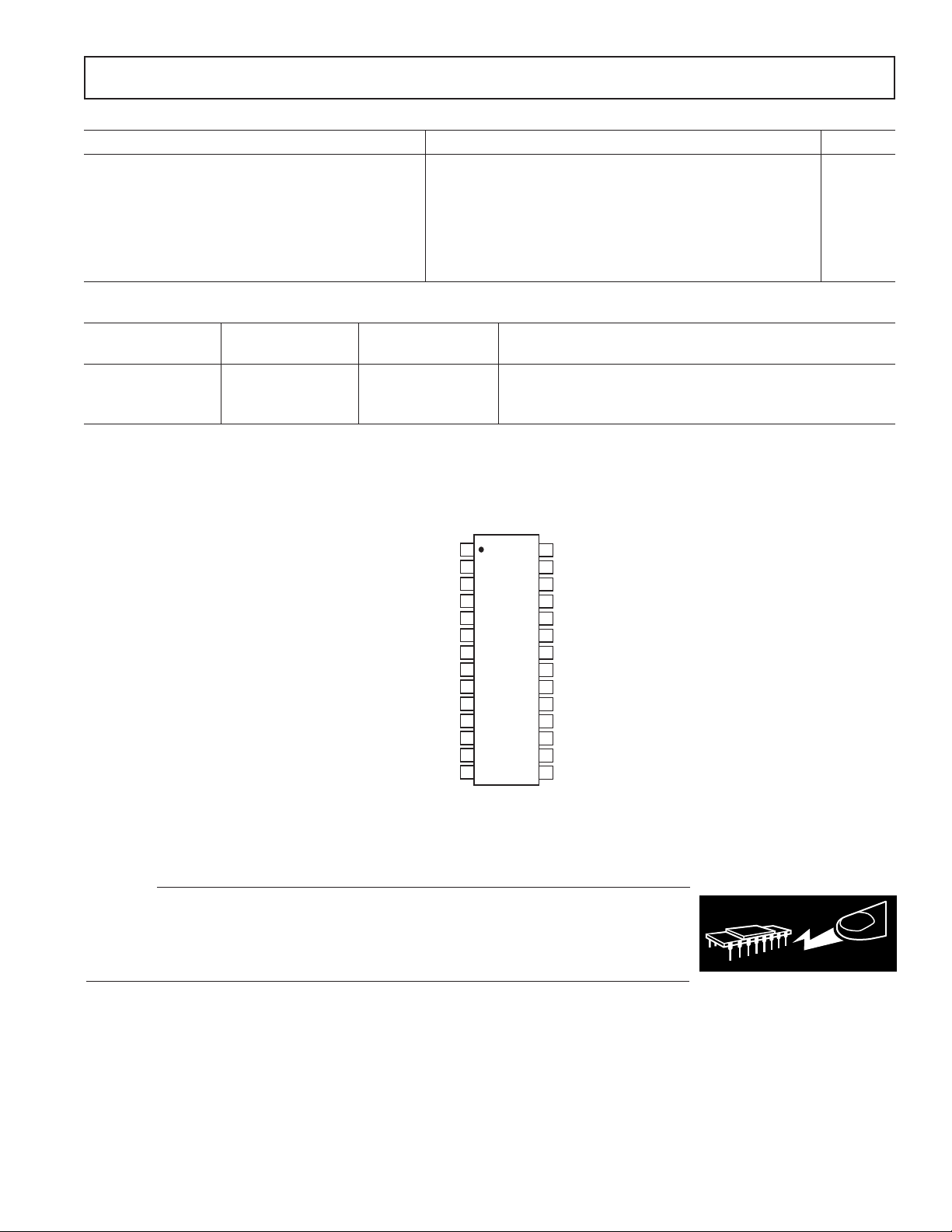
DATA INTERFACE TIMING (STANDALONE MODE–SLAVE)
Mnemonic Description Min Typ Max Unit Comment
t
BCH
t
BCL
t
BDSD
t
LRS
t
LRH
BCLK High Width 30 ns
BCLK Low Width 30 ns
DOUT Delay 20 ns From BCLK Falling
LRCLK Setup 10 ns To BCLK Rising
LRCLK Hold 5 ns From BCLK Rising
BCLK
LRCLK
DOUT
LEFT-JUSTIFIED
MO
DOUT
2
I
S-JUSTIFIED
DE
MO
RIGHT-JUSTIFIED
DOUT
DE
MO
DE
t
BCH
t
LRS
t
BDSD
MSB
8-BIT CLOCKS
(24-BIT DATA)
12-BIT CLOCKS
(20-BIT DATA)
16-BIT CLOCKS
(16-BIT DATA)
t
DBP
t
BCL
MSB–1
MSB
Figure 3. Slave Data Interface Timing
MSB
LSB
–6–
REV. 0
Page 7
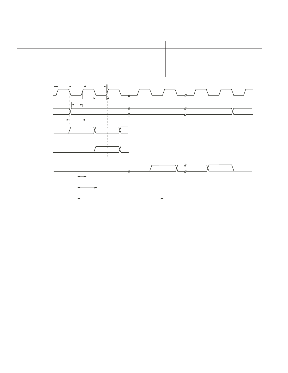
DATA INTERFACE TIMING (CASCADE MODE–MASTER)
Mnemonic Description Min Typ Max Unit Comment
t
BCHDC
t
BCLDC
t
BLRDC
t
BDDC
t
BDIS
t
BDIH
BCLK High Delay 20 ns From MCLK Rising
BCLK Low Delay 20 ns From MCLK Falling
LRCLK Delay 10 ns From BCLK Rising
DOUT Delay 10 ns From BCLK Rising
DIN Setup 10 ns To BCLK Rising
DIN Hold 10 ns From BCLK Rising
MCLK
t
BCHDC
LRCLK
BCLK
DOUT
t
BLRDC
t
t
BDDC
BCLDC
Figure 4. Master Cascade Interface Timing
DATA INTERFACE TIMING (CASCADE MODE–SLAVE)
Mnemonic Description Min Typ Max Unit Comment
t
BCHC
t
BCLC
t
BDSDC
t
LRSC
t
LRHC
t
BDIS
t
BDIH
BCLK High Width 30 ns
BCLK Low Width 30 ns
DOUT Delay 20 ns From BCLK Rising
LRCLK Setup 10 ns To BCLK Rising
LRCLK Hold 5 ns From BCLK Rising
DIN Setup 10 ns To BCLK Rising
DIN Hold 10 ns From BCLK Rising
AD1871
t
t
LRHC
LRSC
t
BDSDC
t
BCHC
t
BCLC
LRCLK
BCLK
DOUT
Figure 5. Slave Cascade Interface Timing
DATA INTERFACE TIMING (MODULATOR MODE)
Mnemonic Description Min Typ Max Unit Comment
t
MOCH
t
MOCL
t
MHDD
t
MLDD
t
MMDR
t
MMDF
MODCLK High Width MCLK ns
MODCLK Low Width MCLK ns
MOD DATA High Delay 30 ns From MCLK Rising
MOD DATA Low Delay 20 ns From MCLK Falling
MODCLK Delay Rising 30 ns MCLK Falling to MODCLK Rising
MODCLK Delay Falling 20 ns MCLK Falling to MODCLK Falling
t
MOCH
MODCLK
t
MOCL
D[0– 3 ]
t
MLDD
t
MHDD
Figure 6. Modulator Mode Timing
REV. 0
–7–
Page 8
AD1871
CONTROL INTERFACE (SPI) TIMING
Mnemonic Description Min Typ Max Unit Comment
t
CCH
t
CCL
t
CCP
t
CDS
t
CDH
t
CLS
t
CLH
t
COE
t
COD
t
COTS
CCLK High Width 40 ns
CCLK Low Width 40 ns
CCLK Period 80 ns
CDATA Setup Time 10 ns To CCLK Rising
CDATA Hold Time 10 ns From CCLK Rising
CLATCH Setup Time 10 ns To CCLK Rising
CLATCH Hold Time 10 ns From CCLK Rising
COUT Enable 15 ns From CLATCH Falling
COUT Delay 20 ns From CCLK Falling
COUT Three-State 25 ns From CLATCH Rising
t
CCH
CCLK
CLATCH
CIN
COUT
D15 D14 D12 D11 D10 D07 D06 D04 D03 D02 D01 D00D13 D09
t
CCL
t
CSU
D08
D08 D07 D06 D05 D04 D03 D02 D01 D00D09
t
t
CHD
CCL
D05
Figure 7. Control Interface Timing
t
CLH
DIGITAL I/O
Parameter Min Typ Max Unit
Input Voltage High (V
Input Voltage Low (V
Input Leakage (I
Input Leakage (I
IH
IL
Output Voltage High (V
Output Voltage Low (V
) 2.4 V
IH
) 0.8 V
IL
@ VIH = 5 V) 10 mA
@ VIL = 0 V) 10 mA
@ IOH = –2 mA) ODVDD – 0.4 V V
OH
@ IOL = +2 mA) 0.4 V
OL
Input Capacitance 15 pF
POWER
Parameter Min Typ Max Unit
Supplies
Voltage, AVDD, and DVDD 4.5 5 5.5 V
Voltage, ODVDD 2.7 5.5 V
Analog Current 40 45 mA
Analog Current—Power-Down (MCLK Running) 4.0 6.0 mA
Digital Current, DVDD 18 22 mA
Digital Current, ODVDD 0.5 1.0 mA
Digital Current—Power-Down (MCLK Running) DVDD* 0.8 2.0 mA
Digital Current—Power-Down (MCLK Running) ODVDD* 1.0 15.0 mA
Power Supply Rejection
1 kHz 300 mV p-p Signal at Analog Supply Pins –86 dB
20 kHz 300 mV p-p Signal at Analog Supply Pins –77 dB
*RESET held low.
TEMPERATURE RANGE
Parameter Min Typ Max Unit
Specifications Guaranteed 25 ∞C
Functionality Guaranteed –40 +105 ∞C
Storage –65 +150 ∞C
Specifications subject to change without notice.
–8–
REV. 0
Page 9
AD1871
ABSOLUTE MAXIMUM RATINGS
Min Typ Max Unit
DVDD to DGND and ODVDD to DGND 0 6 V
AVDD to AGND 0 6 V
Digital Inputs DGND – 0.3 DVDD + 0.3 V
Analog Inputs AGND – 0.3 AVDD + 0.3 V
AGND to DGND –0.3 +0.3 V
Reference Voltage Indefinite Short Circuit to Ground
Soldering (10 sec) 300 ∞C
ORDERING GUIDE
Package Package
Model Temperature Description Option
AD1871YRS –40∞C to +105∞C SSOP RS-28
AD1871YRS-REEL –40∞C to +105∞C SSOP RS-28 in 13” Reel (1500 pieces)
EVAL-AD1871EB Evaluation Board
PIN CONFIGURATION
MCLK
CCLK/(256/512)
COUT/(DF0)
CIN/(DF1)
CLATCH/(M/S)
DVDD
DGND
XCTRL
AVDD
VINLN
VINLP
CAPLN
CAPLP
VREF
1
2
3
4
5
6
AD1871
7
TOP VIEW
(Not to Scale)
8
9
10
11
12
13
14
28
27
26
25
24
23
22
21
20
19
18
17
16
15
LRCLK
BCLK
DOUT
DIN
RESET
ODVDD
DGND
CASC
AGND
VINRN
VINRP
CAPRN
CAPRP
AGND
CAUTION
ESD (electrostatic discharge) sensitive device. Electrostatic charges as high as 4000 V readily
accumulate on the human body and test equipment and can discharge without detection. Although
the AD1871 features proprietary ESD protection circuitry, permanent damage may occur on
devices subjected to high energy electrostatic discharges. Therefore, proper ESD precautions are
recommended to avoid performance degradation or loss of functionality.
WARNING!
ESD SENSITIVE DEVICE
REV. 0
–9–
Page 10

AD1871
PIN FUNCTION DESCRIPTIONS
Pin Input/
No. Output Mnemonic Description
1I MCLK Master Clock. The master clock input determines the sample rate of the device. MCLK
2I CCLK
3 I/O COUT
4I CIN
5I CLATCH
1
1, 2
1
1
6I DVDD 5 V Digital Core Supply
7I DGND Digital Ground
8I XCTRL External Control Enable. This pin is used to select the Control Mode for the device.
9I AVDD 5 V Analog Supply
10 I VINLN Left Channel, Negative Input (via MUX/PGA)
11 I VINLP Left Channel, Positive Input (via MUX/PGA)
12 I/O CAPLN Left External Filter Capacitor (Negative Input to Modulator)
13 I/O CAPLP Left External Filter Capacitor (Positive Input to Modulator)
14 O VREF
15 I AGND Analog Ground
16 I/O CAPRP Right External Filter Capacitor (Positive Input to Modulator)
17 I/O CAPRN Right External Filter Capacitor (Negative Input to Modulator)
18 I VINRP Right Channel, Positive Input (via MUX/PGA)
19 I VINRN Right Channel, Negative Input (via MUX/PGA)
20 I AGND Analog Ground
21 I CASC Cascade Enable. This pin enables cascading of up to four AD1871 devices to a single
22 I DGND Digital Ground
23 I ODVDD
24 I RESET Reset
25 I/O DIN
26 O DOUT
27 I/O BCLK
28 I/O LRCLK
NOTES
1
External Control Mode (See pg 11)
2
Modulator Mode (See pg 11)
2
2
2
2
can be 256, 512, or 768 times the sampling frequency.
Control Port Bit Clock—clock signal for control port (SPI) interface. This pin is reconfigured in the External Control Mode (Pin XCTRL is high), see below.
Control Port Data Out—serial data output from the control port (SPI) interface (in readback). This pin is reconfigured in the External Control Mode (Pin XCTRL is high), see
below; or in Modulator Mode (Bit MME of Control Register II is set), see below.
Control Port Data Input—serial data input for control port (SPI) interface. This pin is
reconfigured in the External Control Mode (Pin XCTRL is high), see below.
Control Port Frame Sync—frame sync (framing signal) for control port (SPI) interface.
This pin is reconfigured in the External Control Mode (Pin XCTRL is high), see below.
When XCTRL is low, control is via the SPI compatible control port (Pins CCLK, CLATCH,
CIN, and COUT). When XCTRL is enabled (high), control of several device functions
is possible by hardware pin strapping (Pins 256/512, M/S, DF1, and DF0). In
External
Control Mode, all other functions are in default state (please refer to the Control Register
Descriptions and External Control section).
Reference Voltage Output. It is recommended to connect a capacitor combination of 10 mF
in parallel with 0.1 mF between VREF and AGND (Pin 15). (See Layout Recommendations.)
DSP serial port (see Cascading section).
Digital Interface Supply. The digital interface can operate from 3.3 V to 5.0 V (nominal).
Serial Data Input. Serial data input pin, only valid when the device is configured in Cascade Mode (Pin CASC is high). This pin is reconfigured in Modulator Mode (Bit MME
of Control Register II is set), see below.
Audio Serial Data Output. This pin is reconfigured in Modulator Mode (Bit MME of
Control Register II is set), see below.
Audio Serial Bit Clock. The bit clock is the audio data serial clock and determines the
rate of audio data transfer. This pin is reconfigured in Modulator Mode (Bit MME of
Control Register II is set), see below.
Left/Right Clock. This clock, also known as the word clock, determines the sampling rate.
It is an output or input depending on the status of Master/Slave. This pin is reconfigured
in Modulator Mode (Bit MME of Control Register II is set), see below.
–10–
REV. 0
Page 11

AD1871
Pin Function Redefinition in External Control Mode
Pin Input/
No. Output Mnemonic Description
2I 256/512 Clock Rate Select. This pin is used to select between an MCLK of 256 f
512 f
3I DF0 Data Format Select 0. This pin is used as the low bit (DF0) of the data format selection
(see section on External Control).
4I DF1 Data Format Select 1. This pin is used as the high bit (DF1) of the data format selection
(see section on External Control).
5I M/S Master/Slave Select. This pin is used to select between the Master (pin low) or Slave (pin
high) Modes.
Pin Function Redefinition in Modulator Mode
Pin Input/
No. Output Mnemonic Description
3O MODCLK
25 O D3 Bit 3 of the Modulator Output Word
26 O D2 Bit 2 of the Modulator Output Word
27 O D1 Bit 1 of the Modulator Output Word
28 O D0 Bit 0 of the Modulator Output Word
This pin provides a clock output that allows the user to decode the left and right channel
modulator outputs. It is similar to a left/right clock but runs (nominally) at 5.6448 MHz
and gates a 4-bit modulator output word in each phase (see section on Modulator Mode).
(pin high).
S
(pin low) or
S
REV. 0
–11–
Page 12

AD1871
TERMINOLOGY
Dynamic Range
The ratio of a full-scale input signal to the integrated input
noise in the pass band (20 Hz to 20 kHz), expressed in decibels
(dB). Dynamic range is measured with a –60 dB input signal
and is equal to (S/[THD+N]) + 60 dB. Note that spurious
harmonics are below the noise with a –60 dB input, so the
noise level establishes the dynamic range. The dynamic range
is specified with and without an A-Weight filter applied.
Signal to (Total Harmonic Distortion + Noise)
(S/[THD+N])
The ratio of the root-mean-square (rms) value of the fundamental input signal to the rms sum of all other spectral components
in the pass band, expressed in decibels (dB).
Pass Band
The region of the frequency spectrum unaffected by the attenuation of the digital decimator’s filter.
Pass-Band Ripple
The peak-to-peak variation in amplitude response from equalamplitude input signal frequencies within the pass band, expressed
in decibels.
Stop Band
The region of the frequency spectrum attenuated by the digital
decimator’s filter to the degree specified by stop-band attenuation.
Gain Error
With a near full-scale input, the ratio of the actual output to the
expected output, expressed as a percentage.
Interchannel Gain Mismatch
With identical near full-scale inputs, the ratio of the outputs of
Crosstalk (EIAJ Method)
Ratio of response on one channel with a grounded input to a
full-scale 1 kHz sine-wave input on the other channel, expressed
in decibels.
Power Supply Rejection
With no analog input, signal present at the output when a
300 mV p-p signal is applied to power supply pins, expressed in
decibels of full scale.
Group Delay
Intuitively, the time interval required for an input pulse to
appear at the converter’s output, expressed in milliseconds (ms).
More precisely, the derivative of radian phase with respect to
radian frequency at a given frequency.
GLOSSARY
ADC—Analog-to-Digital Converter
DSP—Digital Signal Processor
IMCLK—Internal master clock signal, used to clock the decimating filter section. (Its frequency must be 256 ¥ f
MCLK—External master clock signal applied to the AD1871.
Its frequency can be 256, 512, or 768 ¥ f
internally to give an IMCLK frequency that must be 256 ¥ f
MODCLK—This is the - modulator clock that determines
the sample rate of the modulator. Ideally, it should not exceed
the lower of 6.144 MHz or 128 ¥ f
from the IMCLK by a divider that can be selected as /2 or /4.
MUX—Multiplexer
PGA—Programmable Gain Amplifier
the two stereo channels, expressed in decibels.
Gain Drift
Change in response to a near full-scale input with a change in
temperature, expressed as parts-per-million (ppm) per ∞C.
)
S.
. MCLK is divided
S
. The MODCLK is derived
S
.
S
–12–
REV. 0
Page 13

FILTER RESPONSES
Typical Performance Characteristics–AD1871
0
–20
–40
–60
–80
–100
MAGNITUDE – dB
–120
–140
–160
0155
FREQUENCY – NORMALIZED TO
10
TPC 1. Sinc Filter Response (AMC = 0)
0
–20
–40
–60
–80
–100
MAGNITUDE – dB
–120
–140
0
–20
–40
–60
–80
–100
MAGNITUDE – dB
–120
–140
–160
f
S
0155
FREQUENCY – NORMALIZED TO f
10
S
TPC 4. Second Half-Band Filter Response
0
–50
–100
MAGNITUDE – dB
–150
–160
0155
FREQUENCY – NORMALIZED TO
10
f
S
TPC 2. First Half-Band Filter Response
0
–20
–40
–60
–80
–100
MAGNITUDE – dB
–120
–140
–160
0155
FREQUENCY – NORMALIZED TO
10
f
S
TPC 3. Comb Compensation Filter Response
0
51015
FREQUENCY – NORMALIZED TO f
S
TPC 5. Composite Filter Response (AMC = 0)
0
–50
MAGNITUDE – dB
–100
–150
0
0.5 1.0 1.5 2.0
FREQUENCY – NORMALIZED TO
f
S
TPC 6. Composite Filter Response (Pass Band Section)
(AMC = 0)
REV. 0
REV. 0
–13–
Page 14

AD1871
DEVICE PERFORMANCE CURVES
5
0
–5
–10
–15
MAGNITUDE – dB
–20
–25
–30
0
5101520
FREQUENCY – Hz
TPC 7. High-Pass Filter Response, fS = 48 kHz
5
0
–5
–10
–15
MAGNITUDE – dB
–20
–25
–30
0
5101520
FREQUENCY – Hz
0
–20
–40
–60
–80
dBFS
–100
–120
–140
–160
–180
4681012 14 16 18
kHz
202
TPC 10. 1 kHz Tone at –20 dBFS, (32 k-Point FFT), fS = 48 kHz
0
–20
–40
–60
–80
dBFS
–100
–120
–140
–160
–180
4681012141618
kHz
202
TPC 8. High-Pass Filter Response, fS = 96 kHz
0
–20
–40
–60
–80
dBFS
–100
–120
–140
–160
–180
468101214 16 18
kHz
202
TPC 9. 1 kHz Tone at –0.5 dBFS, (32 k-Point FFT), fS = 48 kHz
TPC 11. 1 kHz Tone at –60 dBFS, (32 k-Point FFT),
= 48 kHz
f
S
–20
–30
–40
–50
–60
dB
–70
–80
–90
–100
dBr
–15–60 –55 –50 –45 –40 –35 –30 –25 –20 –10 –5
TPC 12. THD+N vs. Input Amplitude at 1 kHz, fS = 48 kHz
–14–
REV. 0
Page 15

AD1871
–60
–70
–80
dBFS
–90
–100
–110
4681012141618
kHz
202
TPC 13. THD+N vs. Input Frequency at –0.5 dBFS, fS = 48 kHz
–90
–95
–100
–105
dB
0
–10
–20
–30
–40
–50
–60
–70
dB
–80
–90
–100
–110
–120
–130
–140
–150
00.20.40.6 0.8 1.0 1.2 1.4 1.6 1.8 2.0 2.2 2.4 2.6 2.8 3.1
FREQUENCY–MHz
TPC 15. FFT of Modulator Output at –0.5 dBFS, fS = 6.144 MHz
–110
–115
–120
4681012 14 16 18
kHz
202
TPC 14. Channel Separation vs. Frequency at –0.5 dBFS, f
= 48 kHz
S
REV. 0
–15–
Page 16

AD1871
FUNCTIONAL DESCRIPTION
Clocking Scheme
The MCLK pin is the input for the master clock frequency to
the device. Nominally the MCLK frequency will be 256 ¥ f
S
for
correct operation of the device. However, if the user’s MCLK is
a multiple of 256 ¥ f
(perhaps 512 ¥ fS or 768 ¥ fS), it is possible
S
to divide down the MCLK frequency to a suitable internal master
clock frequency (IMCLK) using the MCLK divider block as
AMC BIT
(CONT REG I)
0/1
ANALOG
INPUT
IMCLK
DIVIDER
MCLK
DIVIDER
MODULATOR
6.144MHz
12.288MHz/
24.576MHz
/1 /2 /3
⌺-⌬
/2
/4
6.144MHz
MODCLK
IMCLK
SINC
FILTER
384kHz/
768kHz
shown in Figure 8. The divide options can be chosen from passthrough (/1), /2, or /3 corresponding with 256 ¥ f
768 ¥ f
MCLKs, respectively. The MCLK divider can be con-
S
, 512 ¥ fS, or
S
trolled using the MCD1–MCD0 Bits of Control Register III.
(see Table XIII.)
The resulting internal MCLK (IMCLK) is used to run the
decimating and filtering engine and must be chosen to be at a
48kHz/
96kHz
.
S
HPE BIT
(CONT REG I)
HIGH-PASS
FILTERS
48kHz/
96kHz
ratio of 256 ¥ f
HALF-BAND
FILTERS
MCLK
Figure 8. Clocking Scheme to Modulator and Filter Engine
Modulator
The AD1871’s analog - modulator section comprises a
second order multibit implementation using Analog Device’s
proprietary technology for best performance. As shown in
Figure 9, the two analog integrator blocks are followed by a
Flash ADC section that generates the multibit samples. The
output of the Flash ADC, which is thermometer encoded, is decoded
to binary for output to the filter sections and is scrambled for
feedback to the two integrator stages.
The modulator is optimized for operation at a sampling rate
of 6.144 MHz (which is 128 ¥ f
64 ¥ f
at 96 kHz sampling). The modulator clock control
S
at 48 kHz sampling and
S
(AMC Bit in Control Register I) is used to select the modulator
FROM
ANALOG
INPUT
SECTION
FEEDBACK DACs
兰兰
Figure 9. Modulator Block Diagram
clock (MODCLK) as a ratio from the IMCLK. The modulator
clock divider options are /2 (default) for 48 kHz operation and
/4 for 96 kHz operation. When operating with an IMCLK
of
12.288 MHz, the default divider setting (/2) gives a modulator clock
of 6.144 MHz. When operating with an IMCLK of 24.576 MHz,
the alternate divider setting (/4) gives a modulator clock of
6.144 MHz (see Figure 8).
If it is required to operate the device at a different output sample
rate than those detailed above, perhaps 44.1 kHz or 88.2 kHz,
the decimation filter cutoff characteristics can then be determined
from the normalized frequency response plot shown in TPC 6.
THERMO-
FLASH
ADC
SCRAMBLER
METER
TO
BINARY
DECODER
DIGITAL
OUTPUT
(4 BITS/6.144MHz)
–16–
REV. 0
Page 17

Digital Decimating Filters
CAPxN
CAPxP
V
CM
VINxP
VINxN
V
CM
CAPxN
CAPxP
V
CM
VINxP
VINxN
V
CM
The filtering and decimation of the AD1871’s modulator data
stream is implemented in an embedded DSP engine. The first
stage of filtering is the sinc filtering, which has selectable decimation (selected by the modulator clock control bit (AMC, see
Modulator section). The default decimation in the sinc stage
provides a sample rate reduction of 16; this corresponds with a
MODCLK rate of 128 ¥ f
. The alternate setting of the AMC
S
Bit gives a sinc decimation factor of 8 that corresponds with a
MODCLK rate of 64 ¥ f
stage is at a rate of 8 ¥ f
. The output of the sinc decimator
S
.
S
The filter engine implements two half-band FIR filter sections
and a sinc compensation stage that together give a further
decimation factor of 8. Please refer to TPCs 1 through 4 for
details on the responses of the sinc and FIR filter sections.
TPC 5 gives the composite response of the sinc and FIR filters.
High-Pass Filter
The AD1871 features an optional high-pass filter section that
provides the ability of rejecting dc from the output data stream.
The high-pass filter is enabled by setting Bit 8 (HPE) of Control
Register I to 1. Please refer to TPC 7 and TPC 8 for details of
the high-pass filter characteristics.
ADC Coding
The ADC’s output data stream is in a two’s complement
encoded format. The word width can be selected from 16 bits,
20 bits, or 24 bits (see Table VI and Table VII). The coding
scheme is detailed in Table I.
Table I. ADC Coding
Code Level
011111.......1111 +Full Scale
000000........0000 0 (Ref Level)
100000........0001 –Full Scale
Analog Input Section
The analog input section comprises a differential PGA stage.
It can also be configured for single-ended inputs, allowing
two such inputs to be selected via a multiplex switch. The
PGA has five gain settings (see Table V) ranging from 0 dB
to 12 dB in 3 dB steps.
In Differential Mode, the VINxP and VINxN input pins are
connected to a pair of inverting amplifiers whose outputs are
connected to the CAPxN and CAPxP pins, respectively.
(See Figure 10.)
AD1871
Figure 10. Differential Analog Input
In Single-Ended Mode, either VINxP or VINxN can be selected
as the input. The pair of input inverting amplifiers is reconfigured as
outputs
and CAPxN (see Figure 11).
The analog input section is enabled (powered ON) by default
on reset. If it is required to bypass the analog input section by
using the modulator input pins (CAPxP and CAPxN) directly,
then the analog input section must be powered down by setting
Bits MER and MEL in Control Register III.
Serial Data Interface
The AD1871’s serial data interface consists of three pins
(LRCLK, BCLK, and SDATA). LRCLK is the framing signal for left and right channel samples and its frequency is
equal to the sampling frequency (f
used to clock the data samples from the AD1871 and its frequency is equal to 64 ¥ f
of the left and right channels). SDATA outputs the left and right
channel sample data coincident with the falling edge of BCLK.
The serial data interface supports all the popular audio interface
standards, such as I
well as the serial interfaces of modern DSPs. The Interface Mode is
selected by programming the Bits DF1–DF0 of Control Register II
(see Tables VI and VIII).
The data sample width can be selected from 16, 20, or 24 bits by
programming Bits WW1–WW0 of Control Register II (see
Tables VI and VII).
a single-ended-to-differential conversion stage. Again the
of the differential section are connected to Pins CAPxP
Figure 11. Single-Ended Analog Input
). BCLK is the serial clock
S
(giving 32 BCLK periods for each
S
2
S, left-justified (LJ), and right-justified (RJ), as
REV. 0
–17–
Page 18

AD1871
I2S Mode
In I2S Mode, the data is left-justified, MSB first, with the MSB
placed in the second BCLK period following the transition of
the LRCLK. A high-to-low transition of the LRCLK signifies
LRCLK
BCLK
DOUT
MSB
MSB–2MSB–1 LSB+2 LSB+1
LEFT CHANNEL
LSB
Figure 12. I2S Mode
LJ Mode
In LJ Mode, the data is left-justified, MSB first, with the MSB
placed in the first BCLK period following the transition of the
LRCLK. A high-to-low transition of the LRCLK signifies the
LRCLK
BCLK
DOUT
MSB
MSB–2MSB–1 LSB+2 LSB+1
LEFT CHANNEL
LSB
the beginning of the left channel data transfer, while a low-tohigh
transition on the LRCLK signifies the beginning of the
right channel data transfer (see Figure 12).
RIGHT CHANNEL
MSB
MSB–2MSB–1
LSB+2 LSB+1
LSB MSB
beginning of the right channel data transfer, while a low-to-high
transition on the LRCLK signifies the beginning of the left
channel data transfer (see Figure 13).
RIGHT CHANNEL
MSB
MSB–2MSB–1
LSB+2 LSB+1
LSB
MSB
MSB–1
Figure 13. Left-Justified Mode
RJ Mode
In RJ Mode, the data is right-justified, LSB last, with the
LSB placed in the last BCLK period preceding the transition
of the LRCLK. A high-to-low transition of the LRCLK signifies
LRCLK
BCLK
DOUT
LSB
LEFT CHANNEL
MSB
MSB–2MSB–1 LSB+2 LSB+1
LSB
Figure 14. Right-Justified Mode
DSP Mode
In DSP Mode, the LRCLK signal becomes a frame sync signal
that pulses high for the BCLK period prior to the MSB (or in
the BCLK period of the previous LSB–32 bits). The data is leftjustified, MSB first, with the MSB placed in the BCLK period
following the LRCLK pulse (see Figure 15).
LRCLK
LEFT CHANNEL
the beginning of the right channel data transfer, while a low-tohigh transition on the LRCLK signifies the beginning of the left
channel data transfer (see Figure 14).
RIGHT CHANNEL
MSB
MSB –1
MSB –2
LSB +2
LSB+1
LSB
In I2S and LJ Modes, since the data is left-justified, differences in
data word-width between the AD1871 and the controller are not
catastrophic since the MSBs are guaranteed to be transferred.
There may, however, be a slight reduction in performance
depending on the scale of the mismatch. In RJ Mode, however,
differences in word-width between the AD1871 and controller
have a catastrophic effect on signal performance as the MSBs
of each sample may be lost due to the mismatch.
RIGHT CHANNEL
BCLK
DOUT
MSB
MSB–1
LSB+2 LSB+1
LSB
Figure 15. DSP Mode
–18–
MSB–1 LSB+2 LSB+1
LSBMSB
MSB
MSB–1
REV. 0
Page 19

AD1871
Cascade Mode
The AD1871 supports cascading of up to four devices in a
daisy-chain configuration to the serial port of a DSP. In Cascade
Mode, each device loads an internal 64-Bit Shift Register with
the
results of the left and right channel conversions. The 64Bit Register is split into two subframes of 32 bits each; the first
for left channel data and the second for right channel data.
The results are left-justified, MSB first within the subframes,
and the word-width setting in Control Register II applies.
Remaining bits within the subframe, beyond the conversion
word-width, are set to zero. Please refer to Figure 16.
Up to four devices can be connected in a daisy chain as shown
in Figure 17. All devices must be set in Cascade Mode by tying
the CASC pin of each device to a logic high. The first device in
the chain (Device 4) has its DIN pin tied to logic low. Its
DOUT pin is connected to the DIN pin of Device 3 whose
DOUT is in turn connected to the DIN pin of Device 2. This
daisy chaining is continued until the DOUT of Device 1 is
connected to the DSP’s serial port RX data line (DR0). The
DSP’s RX serial clock (RXCLK0) is connected to the BCLK
pin of all AD1871 devices and the DSP’s RX frame sync (RFS0)
is connected to the LRCLK pin of all AD1871 devices.
24-BIT RESULT
20-BIT RESULT
16-BIT RESULT 16-BIT RESULT
32-BIT LEFT SUBFRAME 32-BIT RIGHT SUBFRAME
24-BIT RESULT
20-BIT RESULT
64-BIT FRAME
Figure 16. DSP Mode
The DSP can be the master and supply the frame sync and
serial clock to the AD1871s, or one of the AD1871s can be
set as the master with the DSP and all other AD1871s set to
slave. Each sampling period begins with a frame sync being generated either by the DSP or one of the AD1871s, depending on
the Master/Slave selection. The frame-sync pulse causes each
device to load the 64-Bit Data I/O Register with the left and
right ADC results. These results are then clocked toward the
DSP where they are received in the following order: Device 1,
Left; Device 1, Right; Device 2, Left; Device 2, Right; Device 3,
Left; Device 3, Right; Device 4, Left; and Device 4, Right.
The DSP’s serial port must be programmed to accept 32-bit
word lengths regardless of the AD1871 word length. The number
of sample words to be accepted per sample interval will be
determined by the number of AD1871 devices in cascade, up
to a maximum of eight words corresponding with the maximum
number of four devices.
Figure 17 also shows the connection of a separate DSP serial port
interface to the control port (SPI) interface of the cascaded
AD1871s. Again this cascade is implemented as a daisy chain,
where the control words for the four devices are output in
sequence (depending on the hookup – 1, 2, 3, and 4 in the
example) to be latched simultaneously at each device by the
common CLATCH. In this mode, it is necessary to send a
control word for each device (16 bits the number of devices)
from the SPI port of the control host. The CLATCH signal can
be controlled from a separate programmable output line. It is
also possible to have individual read/write of the AD1871s
using separate CLATCH controls for each device.
When using Cascade Mode, the data interface defaults to leftjustified, MSB first data, regardless of the state of the Interface
Mode selection (by SPI or external control).
The timing relationships of the Cascade Mode are shown in
Figure 18.
REV. 0
DT1
DR1
TXCLK1/RXCLK1
TFS1/RFS1
ADSP-21xxx
SHARC DSP
RFS0
RXCLK0
DR0
CCLK
COUT
CLATCH
AD1871 No.1
LRCLK
BCLK
DOUT
CIN
DIN
CCLK
COUT
CLATCH
AD1871 No.2
LRCLK
BCLK
DOUT
Figure 17. DSP Mode
–19–
CIN
DIN
CCLK
COUT
CLATCH
AD1871 No.3
LRCLK
BCLK
DOUT
CIN
DIN
CCLK
COUT
CLATCH
AD1871 No.4
LRCLK
BCLK
DOUT
CIN
DIN
Page 20

AD1871
LRCLK
BCLK
DOUT
BCLK
DOUT
CLATCH
CCLK
CIN
DEVICE 1 DEVICE 2 DEVICE 3 DEVICE 4
MSB
MSB
MSB
–1
123 2324
LEFT CHAN N EL
LSB
–2
LSB
+1
MSB
MSB
MSB
–1
123 2324
RIGHT CH AN N EL
LSB
–2
LSB
+1
Figure 18. Cascade Mode Data Interface Timing
DEVICE 1 DEVICE 2 DEVICE 3 DEVICE 4
CCLK
CIN
MSB
MSB
–1
Figure 19. Cascade Mode Control Port Timing
CONTROL/STATUS REGISTERS
The AD1871’s Operating Mode is set by programming three,
10-bit Control Registers via an SPI compatible port.
details the format of the AD1871
control words, which are 16
Table III
bits wide with a 4-bit address field in Positions 15 through 12,
a Read/Write Bit in Position 11, a Reserved Bit in Position 10,
and 10 bits of register data (corre
ter width) in Positions 9 through 0.
occupy Addresses 0000b through 0010b
sponding to the control regis-
The three control words
in the register map (see
Table II).
The AD1871 also features two readback (status) registers that
can be enabled to track the peak reading on each of the channels (left and right). These 6-bit results are read back via the
SPI compatible port in a 16-bit frame similar to that of the
control words.
LSB
LSB
+1
The SPI compatible control port features four signals (CCLK,
CLATCH, CDATA, and COUT). The CLATCH signal is an
enable line that must be low to allow communication to or from
the control port. The CCLK is the serial clock that clocks in
serial data via the CDATA pin and clocks out serial data via the
COUT pin. Figures 20 and 21 show details of the control port
timing.
Table II. Register Address Map
Address Control Register
0000 Control Register I
0001 Control Register II
0010 Control Register III
0011 Peak Reading Register I
0100 Peak Reading Register II
–20–
REV. 0
Page 21

AD1871
Table III. Control/Status Word Format
15-12 11 10 9 6 5 4 3210
Address R/W Reserved Control/Status Data Bits (9–0)
CCLK
CLATCH
CIN
COUT
D15 D14 D12 D11 D10 D09 D08 D07 D06 D05 D04 D03 D02 D01 D00D13
Figure 20. Writing to Register Using Control Port
CCLK
CLATCH
CIN
COUT
D15 D14 D12 D11 D10 D09 D08 D07 D06 D05 D04 D03 D02 D01 D00D13
D08 D07 D06 D05 D04 D03 D02 D01 D00D09
Figure 21. Reading from Register Using Control Port
Table IV. Control Register I (Address 0000b, Write Only)
15–12 11 10 9 8 7 6 5 4 3 2 1 0
0000 0 0 PRE HPE PD AMC AGL2 AGL1 AGL0 AGR2 AGR1 AGR0
9 PRE Peak Reading Enable (0 = Disabled (Default); 1 = Enabled)
8 HPE High-Pass Filter Enable (0 = Disabled (Default); 1 = Enabled)
7PD Power-Down Control (1 = Power-Down; 0 = Normal Operation (Default))
6 AMC ADC Modulator Clock (1 = 64 ¥ f
; 0 = 128 ¥ fS (Default))
S
5–3 AGL2–AGL0 Input Gain (Left Channel, see Table V)
2–0 AGR2–AGL0 Input Gain (Right Channel, see Table V)
Control Register I
Control Register I contains bit settings for control of analog
front end gain, modulator clock selection, power-down control,
high-pass filtering, and peak hold.
Analog Gain Control
The AD1871 features an optional analog front end with selectable gain. Gain is selected using three control bits for each channel,
giving five separate and independent gain settings on each channel.
Bits 2 through 0 (AGR2–AGR0) set the analog gain for the right
channel, while Bits 5 through 3 (AGL2–AGL0) set the analog
gain for the left channel. Table V shows the analog gain corresponding to the bit settings in AGx2–ADx0.
Table V. Analog Gain Settings
AGx2 AGx1 AGx0 Gain (dB)
000 0 (Default)
001 3
010 6
011 9
100 12
101 0
110 0
111 0
REV. 0
–21–
Page 22

AD1871
Modulator Clock
The modulator clock can be chosen to be either 128 ¥ fS or
64 ¥ f
. The AMC Bit (Bit 6) is used to select the modulator’s
S
clock rate. When AMC is set to 0 (default), the modulator clock
is 128 ¥ f
. Otherwise, if set to 1, the modulator clock is 64 ¥ fS.
S
This bit is normally set depending on whether the desired sampling
frequency is 48 kHz or 96 kHz and is also influenced by the
selected MCLK frequency. Please refer to the Functional
Description section for more information on MCLK selection
and sampling rates.
Power-Down
Power-down of the active clock signals within the AD1871 is
effected by writing a Logic 1 to Bit 7 (PD). In Power-Down
Mode, digital activity is suspended and analog sections are
powered down, with the exception of the reference.
High-Pass Filter
The AD1871’s digital filtering engine allows the insertion of a
high-pass filter (HPF) to effectively block dc signals from the
output digital waveform. Setting Bit 8 (HPE) enables the
high-pass filter. For more details of the HPF, refer to the
Functional Description section.
Peak Reading Enable
The AD1871 has two readback registers that can be enabled
to
store the peak readings of the left and right channel ADC results.
To enable the peak readings to be captured, the Peak Reading
Enable Bit (PRE), Bit 9, must be set to Logic 1. When set to
Logic 0, the peak reading capture is disabled.
Table VI. Control Register II (Address 0001b)
15–12 11 10 9 876 543210
0001 0 0 MME DF1 DF0 WW1 WW0 M/S MUR MUL
9–8 Reserved
7 MME Modulator Mode Enable (0 = Normal Mode (Default), 1 = Mod Mode)
6–5 DF1–DF0 Data Format (See Table VIII)
4–3 WW1–WW0 Word Width (See Table VII)
2 M/S Master/Slave Select (0 = Master Mode (Default); 1 = Slave Mode)
1 MUR Mute Control, Right Channel (0 = Disabled (Default); 1 = Enabled)
0 MUL Mute Control, Left Channel (0 = Disabled (Default); 1 = Enabled)
Control Register II
Control Register II contains bit settings for control of left/right
channel muting, data sample word width, data interface format,
and direct modulator bitstream output.
Mute Control
The left and right data channels can be muted to digital zero by
setting the MUL and MUR Bits (Bits 0 and 1), respectively. If a
channel is muted, its output data stream will remain at digital
zero, regardless of the amplitude of the input signal. Setting the
bit to 1 mutes the channel while setting the bit to 0 restores
normal operation.
Master/Slave Select
The AD1871 can operate as either a slave device or a master
WW1 WW0 Word Width (No. of Bits)
0024 (Default)
0120
1016
11Reserved
Data Format
The AD1871’s serial data interface can be configured from a
choice of popular interface formats, including I
right-justified, or DSP Modes. Bits DF1–DF0 are programmed to
select the interface format (mode) as shown in Table VIII.
device. In Slave Mode, the controller must provide the LRCLK
and BCLK to determine the sample rate and serial bit rate. In
Master Mode, the AD1871 provides the LRCLK and BCLK as
outputs that are applied to the controller. The AD1871 defaults to
Master Mode (M/S is low) on reset.
Word Width
The AD1871 allows the output sample word width to be selected
from 16, 20, and 24 bits wide. Compact disc (CD) compatibility
may require 16 bits, while many modern digital audio formats
require 24-bit sample resolution. Bits WW1–WW0 are programmed
to select the word width. Table VII details the Control Register
Bit settings corresponding to the various word width selections.
DF1 DF0 Interface Mode
00I
01Right-Justified
10DSP
11Left-Justified
*Please refer to the Serial Data Interface section in the Functional
Description for more details on the various interface modes.
Modulator Mode Enable
The AD1871 defaults to the conversion of the analog audio to
linear, PCM-encoded digital outputs. Modulator Mode allows
the user to bypass the digital decimation filter section and access
the multibit sigma-delta modulator outputs directly. When in
this mode, certain pins are redefined (see Modulator Mode) and
the modulator output (at a nominal rate of 128 f
on the modulator data pins (D[0–3]). To enable the Modulator Mode, set the MME Bit to high.
Table VII. Word-Width Settings
2
S, left-justified,
Table VIII. Data Interface Format Settings*
2
S (Default)
) is available
S
–22–
REV. 0
Page 23

AD1871
Table IX. Control Register III (Address 0010b)
15–12 11 10 9 8 7 6 5 4 3 2 1 0
0010 0 0 MCD1 MCD0 SEL SER MEL MXL MER MXR
9–8 Reserved (Should Be Programmed to 0)
7–6 MCD1–MCD0 Master Clock Divider (See Table XIII)
5 SEL Single-Ended Enable, Left Channel (0 = Differential
4 SER Single-Ended Enable, Right Channel (0 = Differential
3 MEL Mux/PGA Disable, Left Channel (0 = Enabled
2 MXL Mux Select, Left Channel (0 = VINLP Selected
1 MER Mux/PGA Disable, Right Channel (0 = Enabled
0 MXR Mux Select, Right Channel (0 = VINRP Selected
(Default)
(Default)
(Default)
(Default)
(Default)
; 1 = Single-Ended)
(Default)
; 1 = Single-Ended)
; 1 = Disabled)
; 1 = VINLN Selected)
; 1 = Disabled)
; 1 = VINRN Selected)
Control Register III
Control Register III contains bit settings for configuration of the
analog input section (both left and right channels).
Mux Enable
The Mux Enable Left (MEL) and Mux Enable Right (MER)
are used to enable the analog buffers. When these bits are set to
1, the analog input buffers are powered down and input signals
must be applied directly to the modulator inputs via the CAPxP
and CAPxN pins. (see Figure 23). When MEL and MER are set
to 0 (default condition after reset), the analog input section is
enabled, (see Table X).
Table X. Mux Control Settings
MEL MER Input Setting
0X
1X
X0
X1
Mux Select
Left Channel
Left Channel
Right Channel
Right Channel
Analog Buffer Enabled
Analog Buffer Disabled
Analog Buffer Enabled
Analog Buffer Disabled
The Mux Select Bits (MXL and MXR for left and right channels,
respectively) are used to select the input from VINxP or VINxN
when the input is configured as single-ended. When MXx is set
to 0, the input is taken from VINxP. When MXx is set to 1, the
input is taken from VINxN, (see Table XI).
Table XI. Mux Select Settings*
MXL MXR Input Setting
0X
1X
X0
X1
*Mux select settings are only valid when single-ended operation is enabled; SEL
and SER are set to 1.
Left Channel
Left Channel
Right Channel
Right Channel
Input from VINLP
Input from VINLN
Input from VINRP
Input from VINRN
Single-Ended Mode Enable
The Single-Ended Mode Enable Bits (SEL and SER for left and
right channels, respectively), when set to 1, are used to configure
single-ended input on VINxP and VINxN (input is selected by
state of MXL and MXR). In this mode, single-ended inputs taken
from either VINxP or VINxN (selected using the Mux Select
Bits—MXL and MXR) are internally converted to a differential
format to be applied to the modulator section (see Table XII).
Table XII. Differential/Single-Ended Select
SEL SER Input Setting
0X
1X
X0
X1
Master Clock Divider
Left Channel
Left Channel
Right Channel
Right Channel
Input Æ Differential
Input Æ Single-Ended
Input Æ Differential
Input Æ Single-Ended
The master clock divider allows the division of the external
MCLK frequency to a more suitable internal master clock
frequency (IMCLK). IMCLK must be 256 ¥ f
the available MCLK is not at 256 ¥ f
but is a multiple of
S
; therefore, if
S
this, the MCD allows conversion of MCLK to a suitable IMCLK
at 256 ¥ f
(see Table XIII).
S
Table XIII. Master Clock Divider Settings
MCD1 MCD0 MCLK Division
00IMCLK = MCLK (/1)
01IMCLK = MCLK/2
10IMCLK = MCLK/3
11IMCLK = MCLK (/1)
REV. 0
–23–
Page 24

AD1871
Table XIV. Peak Reading Register I (Address 0011b, Read-Only)
15–12 11 10 9 87 65 432 10
0011 1 0 A0P5 A0P4 A0P3 A0P2 A0P1 A0P0
9–6 Reserved (Always Set to Zero)
5–0 A0P5–A0P0 Left Channel Peak Reading (Valid Only When PRE = 1)
Table XV. Peak Reading Register II (Address 0100b, Read-Only)
15–12 11 10 9 87 65 432 10
0100 1 0 A1P5 A1P4 A1P3 A1P2 A1P1 A1P0
9–6 Reserved (Always Set to Zero)
5–0 A1P5–A1P0 Right Channel Peak Reading (Valid Only When PRE = 1)
Peak Reading Registers
The Peak Reading Registers are read-only registers that can be
enabled to track-and-hold the peak ADC reading from each
channel. The peak reading feature is enabled by setting Bit PRE
in Control Register I. The peak reading value is contained in the
six LSBs of the 10-bit readback word. The result is binary coded
where each LSB is equivalent to –1 dBFS with all zeros corresponding to full scale (0 dBFS) and all ones corresponding
to –63 dBFS (see Table XVI). When Bit PRE is set, the peak
reading per channel is stored in the appropriate peak register.
Once the register is read, the register value is set to zero and is
updated by subsequent conversions.
Table XVI. Peak Reading Result Format
Code
AxP 5 4 3 2 1 0 Level
000000 0 dBFS
000001 –1 dBFS
000010 –2 dBFS
111110 –62 dBFS
111111 –63 dBFS
A Peak Reading Register read cycle is detailed in Figure 21.
EXTERNAL CONTROL
The AD1871 can be configured for external hardware control of
a subset of the device functionality. This functionality includes
Master/Slave Mode select, MCLK select, and serial data
format select. External control is enabled by tying the XCTRL
Pin high as shown in Figure 22.
V
DD
AD1871
XCTRL
M/S
256/512
DF0
DF1
Figure 22. External Control Configuration
Master/Slave Select
The Master/Slave hardware select (Pin 5, CLATCH/[M/S])
is equivalent to setting the M/S Bit of Control Register II. If set
low, the device is placed in Master Mode, whereby the LRCLK
and BCLK signals are outputs from the AD1871.
When M/S is set high, the device is in Slave Mode, whereby the
LRCK and BCLK signals are inputs to the AD1871.
MCLK Mode Select
The MCLK Mode hardware select (Pin 2, CCLK/[256/512]) is
a subset of the MCLK Mode selection that is determined by
Bits CM1–CM0 of Control Register X. When the hardware pin
is low, the device operates with an MCLK that is 256 ¥ f
pin is set high, the device operates with an MCLK that is 512 ¥ f
Serial Data Format Select
; if the
S
.
S
The Serial Data Format hardware select (Pins 3 and 4, DF0/
COUT and DF1/CIN) is equivalent to setting Bits DF1–DF0 of
Control Register II. See Table VIII.
In External Control Mode, all functions other than those
selected
by the hardware select pins (Master/Slave Mode select,
MCLK select, and Serial Data Format select) are in their
default (power-on) state.
MODULATOR MODE
When the device is in Modulator Mode (MME Bit is set to 1),
the D[0–3] pins are enabled as data outputs, while the COUT
pin becomes MODCLK, a high speed sampling clock (nominally at 128 f
). The MODCLK enables successive data from
S
the left and right channel modulators with left channel modulator data being valid in the low phase of MODCLK, while right
channel modulator data is valid under the high phase of
MODCLK
(see Modulator Mode Timing in Figure 6).
The Modulator Mode is designed to be used for applications
such as direct stream digital (DSD) where modulator data is
stored directly to the recording media without decimation and
filtering to a lower sample rate. DSD is specified at a rate of
64 f
, whereas the AD1871 outputs at 128 fS,
S
requiring an intermediate remodulator that downsamples to
and generates a single-bit output steam.
64 f
S
–24–
REV. 0
Page 25

AD1871
INTERFACING
Analog Interfacing
The analog section of the AD1871 has been designed to offer
flexibility as well as high performance. Users may choose full
differential input directly to the ADC’s - modulator via Pins
CAPxP and CAPxN. Alternatively, when using the on-chip PGA
section, it is also possible to multiplex single-ended inputs on Pins
VINxP and VINxN or to use these pins for full differential input.
Whichever input topology is chosen (direct or via mux/PGA
section), the modulator input pins (CAPxP and CAPxN) require
capacitors to act as dynamic charge storage for the switched
capacitor input section. Component selection for these capacitors
is critical as the input audio signal appears on or across these
capacitors. A high quality dielectric is recommended for these
capacitors multilayer ceramic, NPO or metal film, PPS
for
surface-mounted versions, and polypropylene for through-hole
versions. Indeed, as a general recommendation, high quality
dielectrics should be specified where capacitors are carrying the
input audio signal.
Modulator Direct Input
Figure 23 shows the connection of a single-ended source via an
external single-ended-to-differential converter to the modulator
input of the AD1871. The external amplifier/buffer should have
good slew rate characteristics to meet the dynamic characteristics
of the modulator input that is a switched-capacitor load.
The output of the external amplifier/buffer should be decoupled
from the input capacitors via a 250 W resistor (metal film).
In order to configure the AD1871 for differential input via the
CAPxP and CAPxN pins, the Mux/PGA section must be disabled
by setting the MEL and MER Bits in Control Register III to 1.
120pF
NPO
100pF
1nF
NPO
100pF
NPO
NPO
CAPLN
CAPLP
AD1871
FERRITE
100pF
NPO
10F
5.76k⍀
5.76k⍀
750k⍀
5.76k⍀
OP275
OP275
5.76k⍀
237⍀
237⍀
Left Channel
Control Register I = xx0xGGGxxx, where GGG = the Input Gain
(see Table V).
Control Register III = 00xx1x0Sxx, where S = the SE Channel
Selection.
Right Channel
Control Register I = xx0xxxxGGG, where GGG = the Input Gain
(see Table V).
Control Register III = 00xxx1xx0S, where S = the SE Channel
Selection.
CAPLN
CAPLP
AD1871
VINLP
VINLN
VREF
FERRITE
600Z
100pF
NPO
100pF
NPO
10F
10F
1nF
NPO
100pF
NPO
100nF
Figure 24. Single-Ended Input via PGA Section
PGA Input, Differential
Figure 25 shows the connection of a differential source to the PGA
section of the AD1871. The PGA section is configured as a
differential buffer. The buffered differential outputs are connected internally to the CAPxx pins via a 250 W series resistors.
In order to configure the AD1871 for differential input via the
Mux/PGA, the Control Registers must be configured as follows:
Left Channel
Control Register I = xx0xGGGxxx, where GGG = the Input Gain
(see Table V).
Control Register III = 00xx0x0xxx.
Right Channel
Control Register I = xx0xxxxGGG, where GGG = the Input Gain
(see Table V).
Control Register III = 00xxx0xx0x.
10F
100nF
VREF
Figure 23. Direct Connection to Modulator
PGA Input, Single-Ended
Figure 24 shows the connection of a single-ended source to the
PGA section of the AD1871. The PGA section is configured
for single-ended-to-differential conversion. The differential
outputs are connected internally to the CAPxx pins via 250 W
series resistors.
In order to configure the AD1871 for single-ended input, the
Control Registers must be configured as follows:
REV. 0
–25–
100pF
NPO
1nF
NPO
100pF
NPO
CAPLN
CAPLP
AD1871
10F
10F
10F
100nF
2
3
1
VINLP
VINLN
VREF
Figure 25. Differential Input via PGA Section
Page 26

AD1871
LAYOUT CONSIDERATIONS
In order to operate the AD1871 at its specified performance level,
careful consideration must be given to the layout of the AD1871
and its ancillary circuits. Since the analog inputs to the AD1871
are differential, the voltages in the analog modulator are commonmode voltages. The excellent common-mode rejection of the part
will remove common-mode noise on these inputs. The analog
and digital supplies of the AD1871 are independent and separately pinned out to minimize coupling between the analog and
digital sections of the device. The digital filters will
rejection of broadband noise on
integer multiples of the modulator sampling frequency. The
digital filters also remove noise from the analog inputs provided
the noise source does not saturate the analog modulator.
However, because the resolution of the AD1871’s ADC is high,
and the noise levels from the AD1871 are so low, care must be
taken with regard to grounding and layout.
The printed circuit board that houses the AD1871 should be
designed so the analog and digital sections are separated and
confined to certain sections of the board. The AD1871 pin
selection has been configured such that its analog and digital
interfaces are connected on opposite ends of the package. This
facilitates the use of ground planes that can be easily separated.
A minimum etch technique is generally best for ground planes
as it gives the best shielding. Figure 26 is a view of the ground
plane separation (between analog and digital) in the area
surrounding the AD1871, taken from the layout of the AD1871
Evaluation Board (EVAL-AD1871EB).
the power supplies, except at
provide
the analog inputs. Traces on opposite sides of the board
run at right angles to each other. This will reduce the
feedthrough through the board. A microstrip technique
the best but is not always possible with a double-sided board. In
this technique, the component side of the board is
the ground planes while the signals are placed on the other side.
Good decoupling is important when using high speed devices.
All analog and digital supplies should be decoupled to AGND
and DGND, respectively, with 0.1 mF ceramic capacitors in
parallel with 10 mF tantalum capacitors. To achieve the best
from these decoupling capacitors, they should be placed as close
as possible to the device, ideally right up against it, as shown in
Figure 28. In systems where a common supply voltage is used to
drive both the AVDD and DVDD of the AD1871, it is recommended that the system’s AVDD supply be used. This supply
should have the recommended analog supply decoupling between
the AVDD pins of the AD1871 and AGND and the recommended
digital supply decoupling capacitors between the DVDD pin
and DGND.
should
effects of
is by far
dedicated to
Figure 27. Connecting Analog and Digital Grounds
*In the above figure, the black area represents the solder side of the layout. The
silkscreen in white is included for clarity.
Digital and analog ground planes should be joined in only one
place. If this connection is close to the device, it is recommended to use a short (0 W resistor) or ferrite bead inductor as
shown in Figure 27. The pads for the ferrite are positioned on
the solder side directly underneath the AD1871 device.
Avoid running digital lines under the device as they may couple
noise onto the die. The analog ground plane should be allowed
to run under the AD1871 to avoid noise coupling. If it is not
possible to use a power supply plane, the power supply lines to
the AD1871 should use as large a trace as possible to provide
low impedance paths and reduce the effects of glitches on the
power supply lines. Fast switching signals, such as clocks, should
be shielded with digital ground to avoid radiating noise to other
sections of the board, and clock signals should never be
Figure 26. Ground Layout
run near
–26–
Figure 28. AD1871 Power Supply Decoupling
Another important consideration is the selection of components
such as capacitors, resistors, and operational amplifiers for
the ancillary circuits. The capacitors that are used should in the
analog audio signal chain should be of NPO dielectric (if ceramic)
or metal film. Figure 28 shows the placement of the CAPxx pin
capacitors relative to the CAPxx pins. The placement is intended
to keep the tracking between the capacitor and the pin as short as
possible while also ensuring that the track length from CAPxP
pin to its capacitor equals that of the CAPxN to its capacitor.
REV. 0
Page 27

OUTLINE DIMENSIONS
28-Lead Shrink Small Outline Package [SSOP]
(RS-28)
Dimensions shown in millimeters
10.50
10.20
9.90
28 15
5.60
8.20
5.30
7.80
5.00
PIN 1
0.05
MIN
1
2.00 MAX
0.65
BSC
14
1.85
1.75
1.65
0.38
0.22
COMPLIANT TO JEDEC STANDARDS MO-150AH
SEATING
PLANE
7.40
0.10
COPLANARITY
0.25
0.09
AD1871
8ⴗ
4ⴗ
0ⴗ
0.95
0.75
0.55
REV. 0
–27–
Page 28

C02644–0–8/02(0)
–28–
PRINTED IN U.S.A.
 Loading...