

Page 1
Serial-Port 16-Bit
a
FEATURES
Single-Chip Integrated ⌺⌬ Digital Audio Stereo Codec
Multiple Channels of Stereo Input and Output
Digital Signal Mixing
On-Chip Speaker and Headphone Drive Capability
Programmable Gain and Attenuation
On-Chip Signal Filters
Digital Interpolation and Decimation
Analog Output Low-Pass
Sample Rates from 5.5 kHz to 48 kHz
44-Lead PLCC Package
Operation from 5 V and Mixed 5 V/3.3 V Supplies
Serial Interface Compatible with ADSP-21xx Fixed-
Point DSPs
Compatible with CS4215 (See Text)
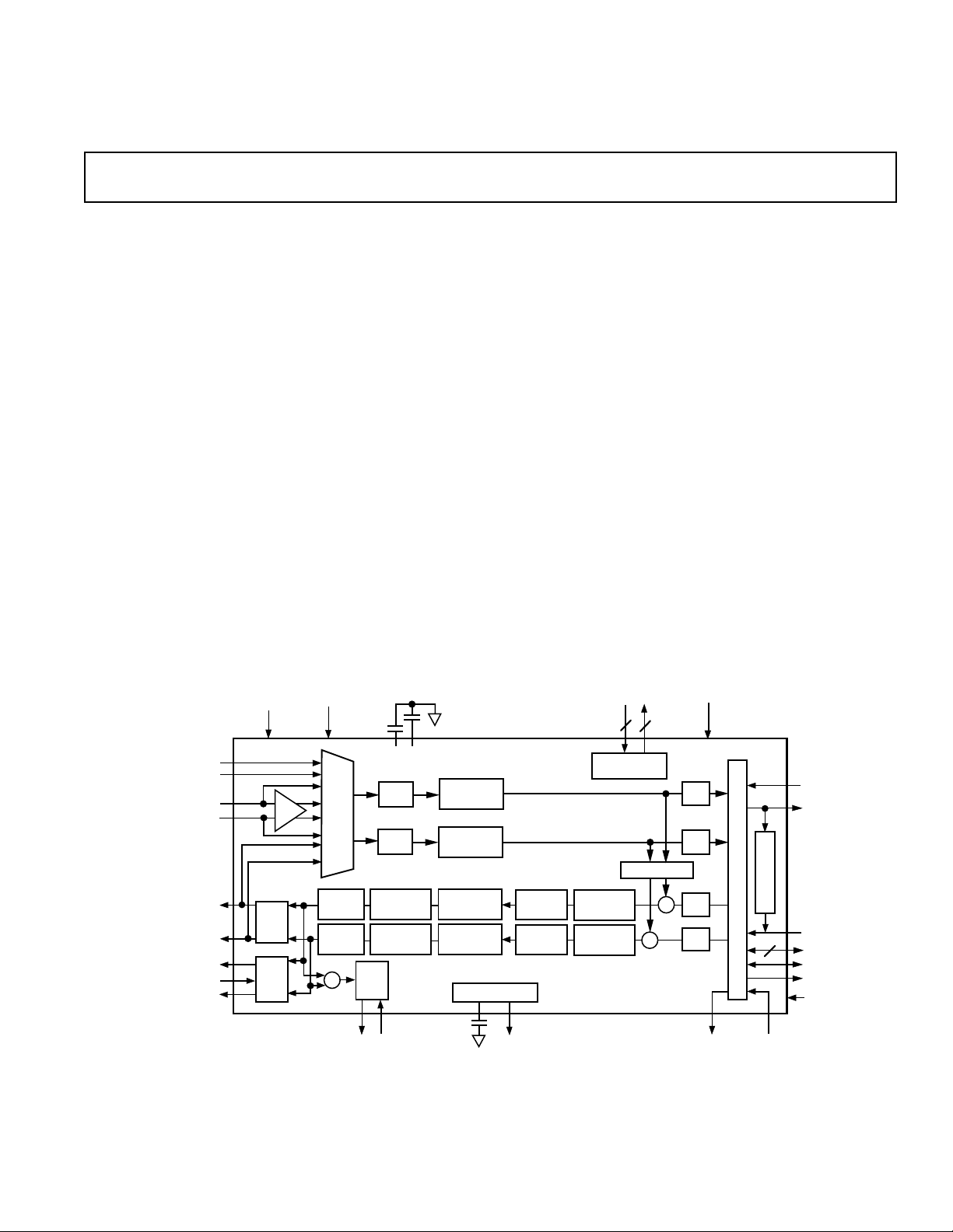
PRODUCT OVERVIEW
The Serial-Port AD1849K SoundPort Stereo Codec integrates
the key audio data conversion and control functions into a single
integrated circuit. The AD1849K is intended to provide a complete, single-chip audio solution for multimedia applications
requiring operation from a single 5 V supply. External signal
path circuit requirements are limited to three low tolerance
capacitors for line level applications; anti-imaging filters are
incorporated on-chip. The AD1849K includes on-chip monaural
®
SoundPort
Stereo Codec
AD1849K
(mono) speaker and stereo headphone drive circuits that require
no additional external components. Dynamic range exceeds
80 dB over the 20 kHz audio band. Sample rates from 5.5 kHz
to 48 kHz are supported from external crystals, from an external
clock, or from the serial interface bit clock.
The Codec includes a stereo pair of Σ∆ analog-to-digital converters
and a stereo pair of Σ∆ digital-to-analog converters. Analog signals
can be input at line levels or microphone levels. A software
controlled programmable gain stage allows independent gain for
each channel going into the ADC. The ADCs’ output can be
digitally mixed with the DACs’ input.
The left and right channel 16-bit outputs from the ADCs are
available over a single bidirectional serial interface that also supports 16-bit digital input to the DACs and control information.
The AD1849K can accept and generate 8-bit µ-law or A-law
companded digital data.
The Σ∆ DACs are preceded by a digital interpolation filter. An
attenuator provides independent user volume control over each
DAC channel. Nyquist images and shaped quantization noise
are removed from the DACs’ analog stereo output by on-chip
switched-capacitor and continuous-time filters. Two independent
stereo pairs of line-level (or one line-level and one headphone)
outputs are generated, as well as drive for a monaural speaker.
FUNCTIONAL BLOCK DIAGRAM
dB
DIGITAL
SUPPLY
L
20
L
R
L
R
MUX
ANALOG
FILTER
ANALOG
FILTER
⌺
OUT RETURN
MONO SPEAKER
GAIN
R
GAIN
ATT EN UAT E
ATT EN UAT E
MUTE
ANALOG
SUPPLY
LINE L
ANALOG
IN
ANALOG
OUT
HEADPHONE RETURN
SoundPort is a registered trademark of Analog Devices, Inc.
LINE R
MIC L
MIC R
LOOPBACK
LINE 0 L
MUTE
LINE 0 R
LINE 1 L
MUTE
LINE 1 R
REV. A
⌺⌬ A/D
CONVERTER
⌺⌬ A/D
CONVERTER
⌺⌬ D/A
CONVERTER
⌺⌬ D/A
CONVERTER
REFERENCE
INTERPOL
INTERPOL ATT EN UAT E
2.25V
ATT EN UAT E
CRYSTALS
2
2
OSCILLATORS
MONITOR MIX
⌺
AD1849K
POWER-DOWN
/A
LAW
/A
LAW
/A
⌺
LAW
/A
LAW
CHAINING
OUTPUT
S
E
R
I
A
L
P
O
R
T
CHAINING
INPUT
L
O
O
P
B
A
C
K
2
DIGITAL
I/O
DATA/CONTROL
MODE
DATA/CONTROL
TRANSMIT
DATA/CONTROL
RECEIVE
PARALLEL I/O
BIT CLOCK
FRAME SYNC
RESET
Information furnished by Analog Devices is believed to be accurate and
reliable. However, no responsibility is assumed by Analog Devices for its
use, nor for any infringements of patents or other rights of third parties
which may result from its use. No license is granted by implication or
otherwise under any patent or patent rights of Analog Devices.
One Technology Way, P.O. Box 9106, Norwood, MA 02062-9106, U.S.A.
Tel: 781/329-4700 World Wide Web Site: http://www.analog.com
Fax: 781/326-8703 © Analog Devices, Inc., 2000
Page 2

AD1849K–SPECIFICATIONS
ELECTRICAL SPECIFICATIONS
STANDARD TEST CONDITIONS UNLESS OTHERWISE NOTED
Temperature 25 °C DAC Input Conditions
Digital Supply (V
Analog Supply (V
Clock (SCLK) 256 F
Master Mode 256 Bits per Frame OLB = 1
Word Rate (F
Input Signal 1 kHz 0 dB PGA Gain
Analog Output Passband 20 Hz to 20 kHz –3.0 dB Relative to Full Scale
V
IH
V
IL
External Load Impedance 10 kΩ
(Line 0)
External Load Impedance 48 Ω
(Line 1)
External Load Capacitance 100 pF
(Line 0, 1)
ANALOG INPUT
Input Voltage*
(RMS Values Assume Sine Wave Input)
Line and Mic with 0 dB Gain 0 94 0.99 1.04 V rms
Mic with 20 dB Gain 0.094 0.099 0.104 V rms
Input Capacitance 15 pF
*Accounts for Sum of Worst Case Reference Errors and Worst Case Gain Errors.
PROGRAMMABLE GAIN AMPLIFIER—ADC
) 5.0 V 0 dB Attenuation
DD
) 5.0 V Full-Scale Digital Inputs
CC
S
) 48 kHz ADC Input Conditions
S
16-Bit Linear Mode
2.4 V Line Input
0.8 V 16-Bit Linear Mode
All tests are performed on all ADC and DAC channels.
Min Typ Max Unit
2.66 2.80 2.94 V p-p
0.266 0.280 0.294 V p-p
Min Typ Max Unit
Step Size (0 dB to 22.5 dB) 1.3 1.5 1.7 dB
(All Steps Tested, –30 dB Input)
PGA Gain Range*
Line and Mic with 0 dB Gain –0.2 +22.7 dB
Mic with 20 dB Gain 19.8 42.7 dB
DIGITAL DECIMATION AND INTERPOLATION FILTERS*
Min Max Unit
Passband 0 0.45 × F
Hz
S
Passband Ripple ± 0.1 dB
Transition Band 0.45 × F
Stopband ≥0.55 × F
S
S
0.55 × F
Hz
S
Hz
Stopband Rejection 74 dB
Group Delay 30/F
S
Group Delay Variation Over Passband 0.0 µs
–2–
REV. A
Page 3
AD1849K
ANALOG-TO-DIGITAL CONVERTERS
Min Typ Max Unit
Resolution* 16 Bits
ADC Dynamic Range, A-Weighted 74 83 dB
Line and Mic with 0 dB Gain (–60 dB Input,
THD+N Referenced to Full Scale)
Mic with 20 dB Gain (–60 dB Input, 72 74 dB
THD+N Referenced to Full Scale)
ADC THD+N, (Referenced to Full Scale)
Line and Mic with 0 dB Gain 0.013 0.020 %
–78 –72 dB
Mic with 20 dB Gain 0.032 0.056 %
–70 –65 dB
ADC Crosstalk
Line to Line (Input L, Ground R, –80 dB
Read R; Input R, Ground L, Read L)
Line to Mic (Input LINL & R, –60 dB
Ground and Select MINL & R,
Read Both Channels)
Gain Error (Full-Scale Span Relative to Nominal) 0.75 dB
ADC Interchannel Gain Mismatch (Line and Mic) 0.3 dB
(Difference of Gain Errors)
DIGITAL-TO-ANALOG CONVERTERS
Min Typ Max Unit
Resolution* 16 Bits
DAC Dynamic Range
(–60 dB Input, THD+N Referenced to Full Scale) 80 86 dB
DAC THD+N (Referenced to Full Scale)
Line 0 and 1 (10 kΩ Load) 0.010 0.020 %
–80 –74 dB
Line 1 (48 Ω Load) 0.022 0.100 %
–73 –60 dB
Mono Speaker (48 Ω Load) 0.045 0.100 %
–67 –60 dB
DAC Crosstalk (Input L, Zero R, Measure –80 dB
LOUT0R and 1R; Input R, Zero L,
Measure LOUT0L and 1L)
Gain Error (Full-Scale Span Relative to Nominal) 0.75 dB
DAC Interchannel Gain Mismatch (Line 0 and 1) 0.3 dB
(Difference of Gain Errors)
Total Out-of-Band Energy* –60 dB
(Measured from 0.55 × FS to 100 kHz)
Audible Out-of-Band Energy* –72 dB
(Measured from 0.55 F
All Selectable Sampling Frequencies)
*Guaranteed, not tested.
to 22 kHz,
S
REV. A
–3–
Page 4
AD1849K
MONITOR MIX ATTENUATOR
Min Typ Max Unit
Step Size (0.0 dB to –60 dB)* 1.3 1.5 1.7 dB
Step Size (–61.5 dB to –94.5 dB)* 1.0 1.5 2.0 dB
Output Attenuation* –95 0.2 dB
DAC ATTENUATOR
Min Typ Max Unit
Step Size (0.0 dB to –60 dB) 1.3 1.5 1.7 dB
(Tested at Steps –1.5 dB, –19.5 dB,
–39 dB and –60 dB)
Step Size (–61.5 dB to –94.5 dB)* 1.0 1.5 2.0 dB
Output Attenuation* –95 0.2 dB
SYSTEM SPECIFICATIONS
Min Typ Max Unit
System Frequency Response* –0.5 +0.2 dB
(Line In to Line Out,
0 to 0.45 × F
Differential Nonlinearity* ± 0.9 LSB
Phase Linearity Deviation* 5 Degrees
)
S
ANALOG OUTPUT
Min Typ Max Unit
Full-Scale Output Voltage (Line 0 & 1) 0.707 V rms
[OLB = 1] 1.85 2.0 2.1 V p-p
Full-Scale Output Voltage (Line 0) 1.0 V rms
[OLB = 0] 2.8 V p-p
Full-Scale Output Voltage (Line 1) 4.0 V p-p
[OLB = 0]
Full-Scale Output Voltage (Mono Speaker) 4.0 V p-p
[OLB = 1]
Full-Scale Output Voltage (Mono Speaker) 8.0 V p-p
[OLB = 0]
CMOUT Voltage (No Load) 1.80 2.25 2.50 V
CMOUT Current Drive* 100 µA
CMOUT Output Impedance 4 kΩ
Mute Attenuation of 0 dB –80 dB
Fundamental* (LINE 0, 1, and MONO)
STATIC DIGITAL SPECIFICATIONS
Min Max Unit
High Level Input Voltage (V
Digital Inputs 2.4 (V
XTAL1/2I 2.4 (V
Low Level Input Voltage (V
High Level Output Voltage (V
Low Level Output Voltage (V
)
IH
) –0.3 +0.8 V
IL
) at IOH = –2 mA 2.4 V
OH
) at IOL = 2 mA 0.4 V
OL
+) + 0.3 V
DD
+) + 0.3 V
DD
Input Leakage Current –10 +10 µA
(GO/NOGO Tested)
Output Leakage Current –10 +10 µA
(GO/NOGO Tested)
*Guaranteed, not tested.
–4–
REV. A
Page 5

DIGITAL TIMING PARAMETERS (Guaranteed over 4.75 V to 5.25 V, 0ⴗC to 70ⴗC)
Min Typ Max Unit
AD1849K
SCLK Period (t
CLK
)
Slave Mode, MS = 0 80 ns
Master Mode, MS = 1* 1/(F
SCLK HI (t
)*
HI
× Bits per Frame) s
S
Slave Mode, MS = 0 25 ns
SCLK LO (t
LO
)*
Slave Mode, MS = 0 25 ns
CLKIN Frequency 13.5 MHz
CLKIN HI 30 ns
CLKIN LO 30 ns
Crystals Frequency 27 MHz
Input Setup Time (t
Input Hold Time (t
Output Delay (t
Output Hold Time (t
Output Hi-Z to Valid (t
Output Valid to Hi-Z (t
)15 ns
S
)10 ns
IH
) 25 ns
D
)0 ns
OH
)15 ns
ZV
) 20 ns
VZ
Power Up RESET LO Time 50 ms
Operating RESET LO Time 100 ns
POWER SUPPLY
Min Typ Max Unit
Power Supply Voltage Range* 4.75 5.25 V
–Digital and Analog
Power Supply Current—Operating 100 130 mA
(50% I
VDD
, 50% I
, Unloaded Outputs)
VCC
Power Supply Current—Power Down 20 200 µA
Power Supply Rejection (@ 1 kHz)* 40 dB
(At Both Analog and Digital
Supply Pins, Both ADCs and DACs)
CLOCK SPECIFICATIONS*
Min Max Unit
Input Clock Frequency, Crystals 27 MHz
Clock Duty Cycle Tolerance ± 10 %
Sample Rate (FS) 5.5125 50 kHz
*Guaranteed, not tested.
Specifications subject to change without notice.
REV. A
–5–
Page 6
AD1849K
ABSOLUTE MAXIMUM RATINGS*
Min Max Unit
Power Supplies
Digital (V
Analog (V
) –0.3 +6.0 V
DD
) –0.3 +6.0 V
CC
Input Current
(Except Supply Pins and MOUT, ± 10.0 mA
MOUTR, LOUT1R, LOUT1L,
LOUT1C)
Analog Input Voltage (Signal Pins) –0.3 (V
Digital Input Voltage (Signal Pins) –0.3 (V
+) + 0.3 V
CC
+) + 0.3 V
DD
Ambient Temperature (Operating) 0 70 °C
Storage Temperature –65 +150 °C
ESD Tolerance (Human Body 500 V
Model per Method 3015.2
of MIL-STD-883B)
*Stresses greater than those listed under Absolute Maximum Ratings may cause
permanent damage to the device. This is a stress rating only; functional operation
of the device at these or any other conditions above those indicated in the
operational section of this specification is not implied. Exposure to absolute
maximum rating conditions for extended periods may affect device reliability.
WARNING: CMOS device. May be susceptible to high-voltage
transient-induced latchup.
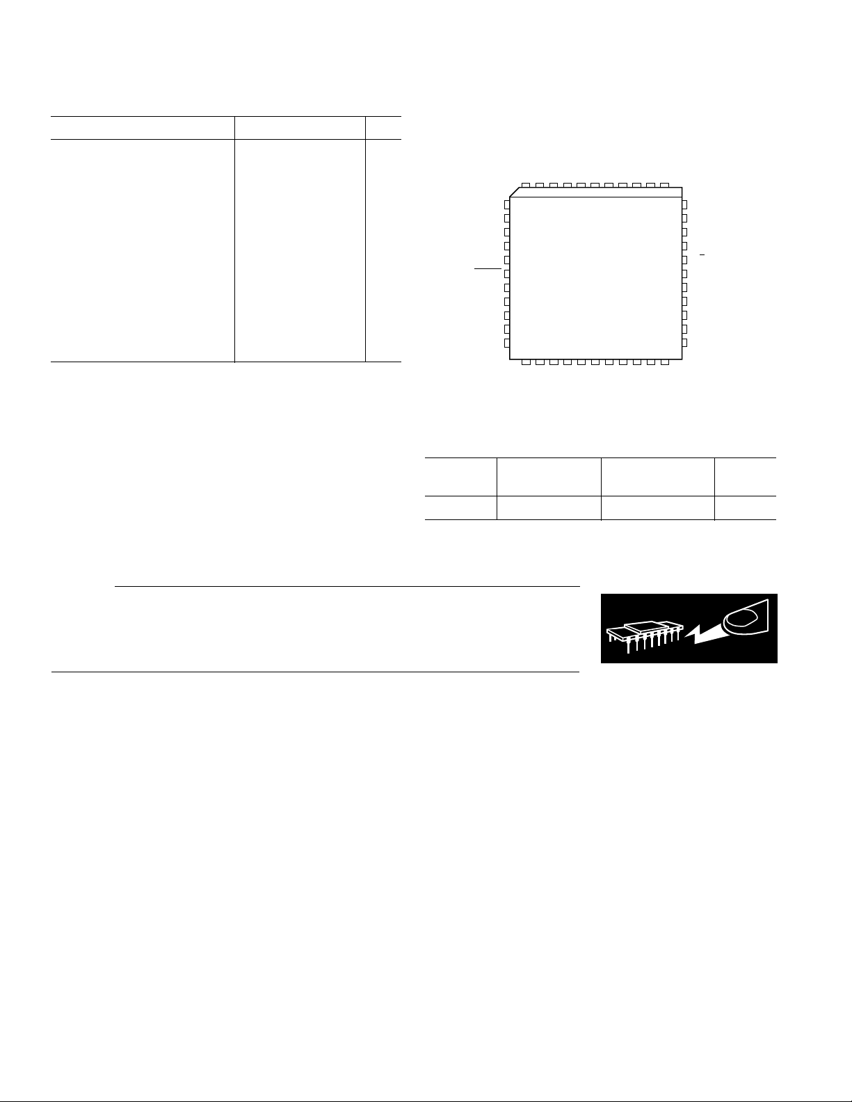
PIN CONFIGURATION
44-Lead Plastic Leaded Chip Carrier
DD
COUT1
V
DD
GNDD
CIN2
COUT2
RESET
PDN
C0
MINR
LINR
MINL
N/C = NO CONNECT
CLKOUT
CLKIN
CIN1
7
17
18
LINL
CMOUT
GNDD
V
1
AD1849KP
SOUNDPORT
STEREO CODEC
C1
REF
V
V
GNDA
SDRX
CC
SDTX
CC
V
FSYNC
SCLK
N/C
GNDA
TSIN
TSOUT
40 6
28
MOUT
MOUTR
39
29
GNDD
V
DD
PIO1
PIO0
D/C
N/C
LOUT0R
LOUT0L
LOUT1L
LOUT1C
LOUT1R
ORDERING GUIDE
Temperature Package Package
Model Range Description Option
AD1849KP 0°C to 70°C 44-Lead PLCC P-44A
CAUTION
ESD (electrostatic discharge) sensitive device. Electrostatic charges as high as 4000 V readily
accumulate on the human body and test equipment and can discharge without detection.
Although the AD1849K features proprietary ESD protection circuitry, permanent damage may
occur on devices subjected to high-energy electrostatic discharges. Therefore, proper ESD
precautions are recommended to avoid performance degradation or loss of functionality.
WARNING!
ESD SENSITIVE DEVICE
–6–
REV. A
Page 7
AD1849K
PIN FUNCTION DESCRIPTIONS
Digital Signals
Pin Name PLCC I/O Description
SDRX 1 I Receive Serial Data Pin
SDTX 44 O Transmit Serial Data Pin
SCLK 43 I/O Bidirectional Serial Bit Clock
FSYNC 42 O Frame Sync Output Signal
TSOUT 41 O Chaining Word Output
TSIN 40 I Chaining Word Input
D/C 35 I Data/Control Select Input
CIN1 6 I Crystal 1 Input
COUT1 7 O Crystal 1 Output
CIN2 10 I Crystal 2 Input
COUT2 11 O Crystal 2 Output
CLKIN 4 I External Sample Clock Input (256 × F
CLKOUT 5 O External Sample Clock Output (256 × F
PDN 13 I Power Down Input (Active HI)
RESET 12 I Reset Input (Active LO)
PIO1 37 I/O Parallel Input/Output Bit 1
PIO0 36 I/O Parallel Input/Output Bit 0
Analog Signals
Pin Name PLCC I/O Description
)
S
)
S
LINL 18 I Left Channel Line Input
LINR 16 I Right Channel Line Input
MINL 17 I Left Channel Microphone Input (–20 dB from Line Level if MB = 0 or Line Level if MB = 1)
MINR 15 I Right Channel Microphone Input (–20 dB from Line Level if MB = 0 or Line Level if MB = 1)
LOUT0L 32 O Left Channel Line Output 0
LOUT0R 33 O Right Channel Line Output 0
LOUT1L 31 O Left Channel Line Output 1
LOUT1R 29 O Right Channel Line Output 1
LOUT1C 30 I Common Return Path for Large Current from External Headphones
MOUT 27 O Mono Speaker Output
MOUTR 28 I Mono Speaker Output Return
C0 14 O External 1.0 µF Capacitor (± 10%) Connection
C1 20 O External 1.0 µF Capacitor (± 10%) Connection
N/C 26 No Connect (Do Not Connect)
N/C 34 No Connect (Do Not Connect)
V
REF
21 O Voltage Reference (Connect to Bypass Capacitor)
CMOUT 19 O Common Mode Reference Datum Output (Nominally 2.25 V)
Power Supplies
Pin Name PLCC I/O Description
V
CC
23 and 24 I Analog Supply Voltage (5 V)
GNDA 22 and 25 I Analog Ground
V
DD
3, 8, 38 I Digital Supply Voltage (5 V)
GNDD 2, 9, 39 I Digital Ground
REV. A
–7–
Page 8

AD1849K
FUNCTIONAL DESCRIPTION
This section overviews the functionality of the AD1849K and
is intended as a general introduction to the capabilities of the
device. As much as possible, detailed reference information has
been placed in “Control Registers” and other sections. The user
is not expected to refer repeatedly to this section.
Analog Inputs
The AD1849K SoundPort Stereo Codec accepts stereo line-level
and mic-level inputs. These analog stereo signals are multiplexed
to the internal programmable gain amplifier (PGA) stage. The
mic inputs can be amplified by 20 dB prior to the PGA to compensate for the voltage swing difference between line levels and
typical condenser microphones. The mic inputs can bypass the
20 dB fixed gain block and go straight to the input multiplexer,
which often results in an improved system signal-to-noise ratio.
The PGA following the input multiplexer allows independent
selectable gains for each channel from 0 to 22.5 dB in 1.5 dB
steps. The Codec can operate either in a global stereo mode or
in a global mono mode with left-channel inputs appearing at
both channel outputs.
Analog-to-Digital Datapath
The AD1849K Σ∆ ADCs incorporate a proprietary fourth-order
modulator. A single pole of passive filtering is all that is required
for antialiasing the analog input because of the ADC’s high 64
times oversampling ratio. The ADCs include linear-phase digital
decimation filters that low-pass filter the input to 0.45 × F
(“FS” is the word rate or “sampling frequency”). ADC input
overrange conditions will cause a sticky bit to be set that can be
read.
Digital-to-Analog Datapath
The Σ∆ DACs are preceded by a programmable attenuator and
a low-pass digital interpolation filter. The attenuator allows
independent control of each DAC channel from 0 dB to –94.5 dB
in 1.5 dB steps plus full digital mute. The anti-imaging interpolation filter oversamples by 64 and digitally filters the higher
frequency images. The DACs’ Σ∆ noise shapers also oversample
by 64 and convert the signal to a single-bit stream. The DAC
outputs are then filtered in the analog domain by a combination
of switched-capacitor and continuous-time filters. They remove
the very high frequency components of the DAC bitstream
output, including both images at the oversampling rate and
shaped quantization noise. No external components are required.
Phase linearity at the analog output is achieved by internally
compensating for the group delay variation of the analog output
filters.
Attenuation settings are specified by control bits in the data
stream. Changes in DAC output level take effect only on zero
crossings of the digital signal, thereby eliminating “zipper”
noise. Each channel has its own independent zero-crossing
detector and attenuator change control circuitry. A timer
guarantees that requested volume changes will occur even in the
absence of an input signal that changes sign. The time-out
period is 10.7 milliseconds at a 48 kHz sampling rate and 64
milliseconds at an 8 kHz sampling rate (Time-out [ms] ≈ 512/
Sampling Rate [kHz]).
S
Monitor Mix
A monitor mix is supported that digitally mixes a portion of the
digitized analog input with the analog output (prior to digitization). The digital output from the ADCs going out of the serial
data port is unaffected by the monitor mix. Along the monitor
mix datapath, the 16-bit linear output from the ADCs is attenuated
by an amount specified with control bits. Both channels of
the monitor data are attenuated by the same amount. (Note
that internally the AD1849K always works with 16-bit PCM
linear data, digital mixing included; format conversions take
place at the input and output.)
Sixteen steps of –6 dB attenuation are supported to –94.5 dB. A
“0” implies no attenuation, while a “14” implies 84 dB of
attenuation. Specifying full scale “15” completely mutes the
monitor datapath, preventing any mixing of the analog input
with the digital input. Note that the level of the mixed output
signal is also a function of the input PGA settings since they
affect the ADCs’ output.
The attenuated monitor data is digitally summed with the DAC
input data prior to the DACs’ datapath attenuators. Because
both stereo signals are mixed before the output attenuators,
mix data is attenuated a second time by the DACs’ datapath
attenuators. The digital sum of digital mix data and DAC
input data is clipped at plus or minus full scale and does not
wrap around.
Analog Outputs
One stereo line-level output, one stereo headphone output, and
one monaural (mono) speaker output are available at external
pins. Each of these outputs can be independently muted. Muting
either the line-level stereo output or the headphone stereo
output mutes both left and right channels of that output. When
muted, the outputs will settle to a dc value near CMOUT,
the midscale reference voltage. The mono speaker output is
differential. The chip can operate either in a global stereo mode
or in a global mono mode with left channel inputs appearing at
both outputs.
Digital Data Types
The AD1849K supports four global data types: 16-bit twoscomplement linear PCM, 8-bit unsigned linear PCM, 8-bit
companded µ-law, and 8-bit companded A-law, as specified by
control register bits. Data in all four formats is always transferred MSB first. Sixteen-bit linear data output from the ADCs
and input to the DACs is in twos-complement format. Eight-bit
data is always left-justified in 16-bit fields; in other words, the
MSBs of all data types are always aligned; in yet other words,
full-scale representations in all three formats correspond to
equivalent full-scale signals. The eight least-significant bit positions
of 8-bit linear and companded data in 16-bit fields are ignored
on input and zeroed on output.
The 16-bit PCM data format is capable of representing 96 dB of
dynamic range. Eight-bit PCM can represent 48 dB of dynamic
range. Companded µ-law and A-law data formats use nonlinear
coding with less precision for large-amplitude signals. The loss
of precision is compensated for by an increase in dynamic range
to 64 dB and 72 dB, respectively.
–8–
REV. A
Page 9
AD1849K
On input, 8-bit companded data is expanded to an internal
linear representation, according to whether µ-law or A-law was
specified in the Codec’s internal registers. Note that when µ-law
compressed data is expanded to a linear format, it requires 14
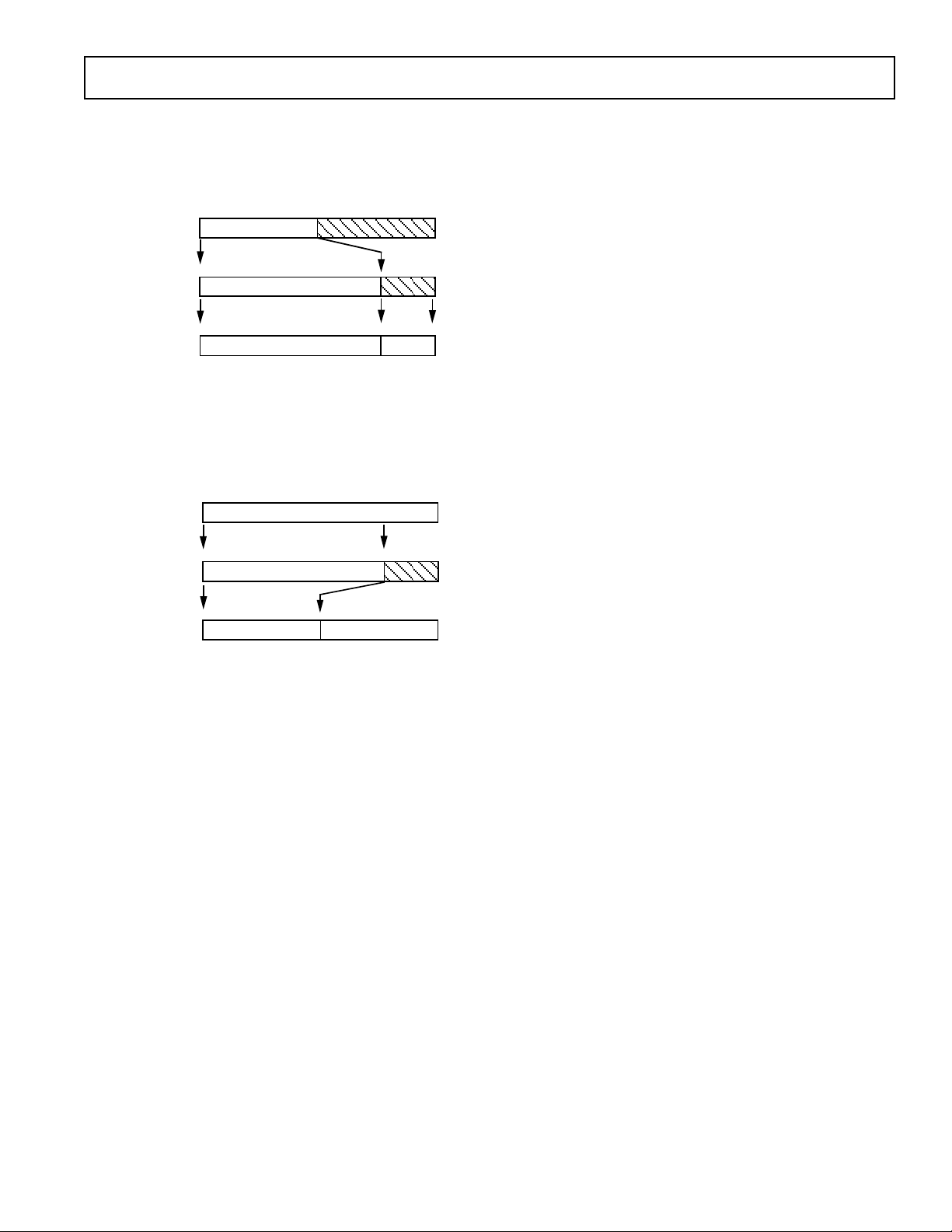
bits. A-law data expanded requires 13 bits, see Figure 1.
COMPRESSED
INPUT DATA
EXPANSION
DAC INPUT
15 0
MSB
15 0
MSB
15 0
MSB
LSB
8 7
3/2 2/1
LSB
3/2 2/1
LSB
0 0 0 / 0 0
Figure 1. A-Law or µ-Law Expansion
When 8-bit companding is specified, the ADCs’ linear output is
compressed to the format specified prior to output. See Figure 2.
Note that all format conversions take place at input or output.
Internally, the AD1849K always uses 16-bit linear PCM
representations to maintain maximum precision.
15 0
ADC OUTPUT
TRUNCATION
COMPRESSION
MSB
15 0
MSB
15 0
MSB
8 7
LSB
3/2
LSB
0 0 0 0 0 0 0 0
LSB
2/1
Figure 2. A-Law or µ-Law Compression
Power Supplies and Voltage Reference
The AD1849K operates from 5 V power supplies. Independent
analog and digital supplies are recommended for optimal
performance, though excellent results can be obtained in single
supply systems. A voltage reference is included on the Codec
and its 2.25 V buffered output is available on an external pin
(CMOUT). The CMOUT output can be used for biasing op
amps used in dc coupling. The internal reference is externally
bypassed to analog ground at the V
pin. Note that V
REF
REF
should only be connected to its bypass capacitors.
Autocalibration
The AD1849K supports an autocalibration sequence to eliminate
DAC and ADC offsets. The autocalibration sequence is
initiated in the transition from Control Mode to Data Mode,
regardless of the state of the AC bit. The user should specify
that analog outputs be muted to prevent undesired outputs.
Monitor mix will be automatically disabled by the Codec.
During the autocalibration sequence, the serial data output from
the ADCs is meaningless and the ADI bit is asserted. Serial data
inputs to the DACs are ignored. Even if the user specified the
muting of all analog outputs, near the end of the autocalibration
sequence, dc analog outputs very close to CMOUT will be
produced at the line outputs and mono speaker output.
An autocalibration sequence is also performed when the
AD1849K leaves the reset state (i.e., RESET goes HI). The
RESET pin should be held LO for 50 ms after power up or after
leaving power-down mode to delay the onset of the autocalibration
sequence until after the voltage reference has settled.
Loopback
Digital and analog loopback modes are supported for device and
system testing. The monitor mix datapath is always available for
loopback test purposes. Additional loopback tests are enabled by
setting the ENL bit (Control Word Bit 33) to a “1.”
Analog loopback mode D-A-D is enabled by setting the ADL
bit (Control Word Bit 32) to a “1” when ENL is a “1.” In this
mode, the DACs’ analog outputs are re-input to the PGAs prior
to the ADCs, allowing digital inputs to be compared to digital
outputs. The monitor mix will be automatically disabled by the
Codec during D-A-D loopback. The analog outputs can be
individually attenuated, and the analog inputs are internally
disconnected. Note that muting the line 0 output mutes the
looped-back signal in this mode.
Digital loopback mode D-D is enabled by resetting the ADL bit
(Control Word Bit 32) to a “0” when ENL is a “1.” In this mode,
the control and data bit pattern presented on the SDRX pin is
echoed on the SDTX pin with a two frame delay, allowing the
host controller to verify the integrity of the serial interface starting
on the third frame after D-D loopback is enabled. During digital
loopback mode, the output DACs are operational.
REV. A
–9–
Page 10

AD1849K
The loopback modes are shown graphically in Figure 3.
LINE, MIC
INPUT
DISCONNECTED
LINE 0,
OUTPUT
LINE 1
FUNCTIONAL
GAIN
AD1849K
MUTE
0
1
A/D
D/A
MONITOR
DISABLE
/A-LAW
ENCODE
/A-LAW
DECODE
Analog Loopback D-A-D
LINE, MIC
INPUT
LINE 0,
LINE 1
OUTPUT
FUNCTIONAL
GAIN
AD1849K
A/D
MONITOR
D/AMUTE
/A-LAW
ENCODE
/A-LAW
ENCODE
Digital Loopback D-D
Figure 3. Loopback Modes
SDTX
SDRX
SDTX
SDRX
Clocks and Sample Rates
The AD1849K can operate from external crystals, from a 256 ×
F
input clock, from an input clock with a programmable divide
S
factor, or from the serial port’s bit clock (at 256 × F
), selected
S
under software control. Two crystal inputs are provided to
generate a wide range of sample rates. The oscillators for these
crystals are on the AD1849K, as is a multiplexer for selecting
between them. They can be overdriven with external clocks by
the user, if so desired. The recommended crystal frequencies are
16.9344 MHz and 24.576 MHz. From them the following sample
rates can be internally generated: 5.5125, 6.615, 8, 9.6, 11.025,
16, 18.9, 22.05, 27.42857, 32, 33.075, 37.8, 44.1, 48 kHz.
Regardless of clock input source, a clock output of 256 × F
is
S
generated (with some skew). If an external input clock or the
serial port’s bit clocks are selected to drive the AD1849K’s
internal operation, they should be low jitter clocks. If no external
clock will be used, Analog Devices recommends tying the clock
input pin (CLKIN) to ground. If either external crystal is not
used, Analog Devices recommends tying its input (CIN1 and/or
CIN2) to ground.
–10–
REV. A
Page 11

AD1849K
CONTROL REGISTERS
The AD1849K SoundPort Stereo Codec accepts control information through its serial port when in Control Mode. Some control
information is also embedded in the data stream when in Data Mode. (See Figure 8.) Control bits can also be read back for system
verification. Operation of the AD1849K is determined by the state of these control bits. The 64-bit serial Control Mode and Data
Mode control registers have been arbitrarily broken down into bytes for ease of description. All control bits initialize to default states
after RESET or Power Down. Those control bits that cannot be changed in Control Mode are initialized to defaults on the transition
from Data Mode to Control Mode. See below for a definition of these defaults.
Control Mode Control Registers
Control Byte 1, Status Register
Data 7 Data 6 Data 5 Data 4 Data 3 Data 2 Data 1 Data 0
001MBOLBDCB0AC
63 62 61 60 59 58 57 56
MB Mic bypass:
0 Mic inputs applied to 20 dB fixed gain block.
1 Mic inputs bypass 20 dB fixed gain block.
OLB Output level bit:
0 Full-scale line 0 output is 2.8 V p-p (1 V rms).
Full-scale line 1 output is 4.0 V p-p.
Full-scale mono speaker output is 8.0 V p-p.
1 Full-scale line 0 output is 2.0 V p-p.
Full-scale line 1 output is 2.0 V p-p.
Full-scale mono speaker output is 4.0 V p-p.
DCB Data/control bit. Used for handshaking in data/control transitions. See “DCB Handshake Protocol.”
AC Autocalibration.
Autocalibration will always occur on the Control-to-Data mode transition. The AC bit is ignored. Autocalibration
requires an interval of 194 frames. Offsets for all channels of ADC and DAC are zeroed. The user should specify that
analog outputs are muted to prevent undesired outputs, i.e., OM0 = “0,” OM1 = “0,” and SM =“0.” Monitor mix will
be automatically disabled by the Codec.
REV. A
–11–
Page 12

AD1849K
Control Byte 2, Data Format Register
Data 7 Data 6 Data 5 Data 4 Data 3 Data 2 Data 1 Data 0
0 0 DFR2 DFR1 DFR0 ST DF1 DF0
55 54 53 52 51 50 49 48
DFR2:0 Data conversion frequency (FS) select tin kHz:
DFR Divide Factor XTAL1 (24.576 MHz) XTAL2 (16.9344 MHz)
0 3072 8 5.5125
1 1536 16 11.025
2 896 27.42857 18.9
3 768 32 22.05
4 448 N/A 37.8
5 384 N/A 44.1
6 512 48 33.075
7 2560 9.6 6.615
Note that the AD1849K’s internal oscillators can be overdriven by external clock sources at the crystal input pins. If an
external clock source is used, it should be applied to the crystal input pin (CIN1 or CIN2), and the crystal output pin
(COUT1 or COUT2) should be left unconnected. The external clock source need not be at the recommended crystal
frequencies, and it will be divided down by the selected Divide Factor.
ST Global stereo mode. Both converters are placed in the same mode.
0 Mono mode. The left analog input appears at both ADC outputs. The left digital input appears at both DAC outputs.
1 Stereo mode
DF1:0 Codec data format selection:
0 16-bit twos-complement PCM linear
1 8-bit µ-law companded
2 8-bit A-law companded
3 8-bit unsigned PCM linear
Control Byte 3, Serial Port Control Register
Data 7 Data 6 Data 5 Data 4 Data 3 Data 2 Data 1 Data 0
ITS MCK2 MCK1 MCK0 FSEL1 FSEL0 MS TXDIS
47 46 45 44 43 42 41 40
ITS Immediate three-state:
0 FSYNC, SDTX and SCLK three-state within 3 SCLK cycles after D/C goes LO
1 FSYNC, SDTX and SCLK three-state immediately after D/C goes LO
MCK2:0 Clock source select for Codec internal operation:
0 Serial bit clock (SCLK) is the master clock at 256 × F
1 24.576 MHz crystal (XTAL1) is the clock source
2 16.9344 MHz crystal (XTAL2) is the clock source
3 External clock (CLKIN) is the clock source at 256 × F
4 External clock (CLKIN) is the clock source, divided by the factor selected by DFR2:0
(External clock must be stable and valid within 2000 periods after it is selected.)
FSEL1:0 Frame size select:
0 64 bits per frame
1 128 bits per frame
2 256 bits per frame
3 Reserved
Note that FSEL is overridden in Data Mode when SCLK is the clock source (MCK = “0”). When SCLK is providing
the 256 × F
clock for internal Codec operation, 256 bits per frame is effectively selected, regardless of FSEL’s contents.
S
MS Master/slave mode for the serial interface:
0 Receive serial clock (SCLK) and TSIN from an external device (“slave mode”)
1 Transmit serial clock (SCLK) and frame sync (FSYNC) to external devices (“master mode”)
Note that MS is overridden when SCLK is the clock source (MCK = “0”). When SCLK is providing the clock for
internal Codec operation, slave mode is effectively selected, regardless of the contents of MS.
TXDIS Transmitter disable:
0 Enable serial output
1 Three-state serial data output (high impedance)
Note that Control Mode overrides TXDIS. In Control Mode, the serial output is always enabled.
S
S
–12–
REV. A
Page 13

Control Byte 4, Test Register
Data 7 Data 6 Data 5 Data 4 Data 3 Data 2 Data 1 Data 0
000000ENLADL
39 38 37 36 35 34 33 32
ENL Enable loopback testing:
0 Disabled
1 Enabled
ADL Loopback mode:
0 Digital loopback from Data/Control receive to Data/Control transmit (D-D)
1 Analog loopback from DACs to ADCs (D-A-D)
Control Byte 5, Parallel Port Register
Data 7 Data 6 Data 5 Data 4 Data 3 Data 2 Data 1 Data 0
PIO1 PIO0 000000
31 30 29 28 27 26 25 24
PIO1:0 Parallel I/O bits for system signaling. PIO bits do not affect Codec operation.
Control Byte 6, Reserved Register
Data 7 Data 6 Data 5 Data 4 Data 3 Data 2 Data 1 Data 0
AD1849K
00000000
23 22 21 20 19 18 17 16
Reserved bits should be written as 0.
Control Byte 7, Revision Register
Data 7 Data 6 Data 5 Data 4 Data 3 Data 2 Data 1 Data 0
0010REVID3 REVID2 REVID1 REVID0
15 14 13 12 11 10 9 8
REVID3:0 Silicon revision identification. Reads greater than or equal to 0010 (i.e., 0010, 0011, etc.) for the AD1849K.
Control Byte 8, Reserved Register
Data 7 Data 6 Data 5 Data 4 Data 3 Data 2 Data 1 Data 0
00000000
76543210
Reserved bits should be written as 0.
REV. A
–13–
Page 14

AD1849K
Data Mode Data and Control Registers
Data Byte 1, Left Audio Data—Most Significant 8 Bits
Data 7 Data 6 Data 5 Data 4 Data 3 Data 2 Data 1 Data 0
L15 L14 L13 L12 L11 L10 L9 L8
63 62 61 60 59 58 57 56
In 16-bit linear PCM mode, this byte contains the upper eight bits of the left audio data sample. In the 8-bit companded and linear
modes, this byte contains the left audio data sample. In mono mode, only the left audio data is used. MSB first format is used in all
modes, and twos-complement coding is used in 16-bit linear PCM mode.
Data Byte 2, Left Audio Data—Least Significant 8 Bits
Data 7 Data 6 Data 5 Data 4 Data 3 Data 2 Data 1 Data 0
L7 L6 L5 L4 L3 L2 L1 L0
55 54 53 52 51` 50 49 48
In 16-bit linear PCM mode, this byte contains the lower eight bits of the left audio data sample. In the 8-bit companded and linear
modes, this byte is ignored on input, zeroed on output. In mono mode, only the left audio data is used. MSB first format is used in
all modes, and twos-complement coding is used in 16-bit linear PCM mode.
Data Byte 3, Right Audio Data—Most Significant 8 Bits
Data 7 Data 6 Data 5 Data 4 Data 3 Data 2 Data 1 Data 0
R15 R14 R13 R12 R11 R10 R9 R8
47 46 45 44 43 42 41 40
In 16-bit linear PCM mode, this byte contains the upper eight bits of the right audio data sample. In the 8-bit companded and linear
modes, this byte contains the right audio data sample. In mono mode, this byte is ignored on input, zeroed on output. MSB first
format is used in all modes, and twos complement coding is used in 16-bit linear PCM mode.
Data Byte 4, Right Audio Data—Least Significant 8 Bits
Data 7 Data 6 Data 5 Data 4 Data 3 Data 2 Data 1 Data 0
R7 R6 R5 R4 R3 R2 R1 R0
39 38 37 36 35 34 33 32
In 16-bit linear PCM mode, this byte contains the lower eight bits of the right audio data sample. In the 8-bit companded and linear
modes, this byte is not used. In mono mode, this byte is ignored on input, zeroed on output. MSB first format is used in all modes,
and twos-complement coding is used in 16-bit linear PCM mode.
Data Byte 5, Output Setting Register 1
Data 7 Data 6 Data 5 Data 4 Data 3 Data 2 Data 1 Data 0
OM1 OM0 LO5 LO4 LO3 LO2 LO1 LO0
31 30 29 28 27 26 25 24
OM1 Output Line 1 Analog Mute:
0 Mute Line 1
1 Line 1 on
OM0 Output Line 0 Analog Mute:
0 Mute Line 0
1 Line 0 on
LO5:0 Output attenuation setting for the left DAC channel; “0” represents no attenuation. Step size is 1.5 dB; “62” represents
93 dB of attenuation. Attenuation = 1.5 dB × LO, except for LO = “63,” which represents full digital mute.
–14–
REV. A
Page 15

AD1849K
Data Byte 6, Output Setting Register 2
Data 7 Data 6 Data 5 Data 4 Data 3 Data 2 Data 1 Data 0
ADI SM RO5 RO4 RO3 RO2 RO1 RO0
23 22 21 20 19 18 17 16
ADI ADC Invalid. This bit is set to “1” during the autocalibration sequence, indicating that the serial data output from the
ADCs is meaningless.
SM Mono Speaker Analog Mute:
0 Mute mono speaker
1 Mono speaker on
RO5:0 Output attenuation setting for the right DAC channel; “0” represents no attenuation. Step size is 1.5 dB; “62”
represents 93 dB of attenuation. Attenuation = 1.5 dB × RO, except for RO = “63,” which represents full digital mute.
Data Byte 7, Input Setting Register 1
Data 7 Data 6 Data 5 Data 4 Data 3 Data 2 Data 1 Data 0
PIO1 PIO0 OVR IS LG3 LG2 LG1 LG0
15 14 13 12 11 10 9 8
PIO1:0 Parallel I/O bits for system signaling. PIO bits do not affect Codec operation.
OVR ADC input overrange. This bit is set to “1” if either ADC channel is driven beyond the specified input range. It is
“sticky,” i.e., it remains set until explicitly cleared by writing a “0” to OVR. A “1” written to OVR is ignored,
allowing OVR to remain “0” until an overrange condition occurs.
IS Input selection:
0 Line-level stereo inputs
1 Microphone (condenser-type) level inputs if MB = 0 (20 dB gain), or line-level stereo inputs if MB = 1
(0 dB gain).
LG3:0 Input gain for left channel. “0” represents no gain. Step size is 1.5 dB; “15” represents 22.5 dB of input gain.
Gain = 1.5 dB × LG.
Data Byte 8, Input Setting Register 2
Data 7 Data 6 Data 5 Data 4 Data 3 Data 2 Data 1 Data 0
MA3 MA2 MA1 MA0 RG3 RG2 RG1 RG0
76543210
MA3:0 Monitor mix. “0” represents no attenuation, i.e., the ADCs’ output is fully mixed with the DACs’ input. Step size
is 6 dB; “14” represents an attenuation of both channels of the ADCs’ output along the monitor datapath of
84 dB. Mix attenuation = 6 dB × MA, except for MA = “15,” which disables monitor mix entirely.
RG3:0 Input gain for right channel. “0” represents no gain. Step size is 1.5 dB; “15” represents 22.5 dB of input gain.
Gain = 1.5 dB × RG.
REV. A
–15–
Page 16

AD1849K
Control Register Defaults
Upon coming out of RESET or Power Down, internal control registers will be initialized to the following values:
Defaults Calming Out of RESET or Power Down
MB 0 Mic Input Applied to 20 dB Fixed Gain Block
OLB 0 Full-Scale Line 0 Output 2.8 V p-p, Full-Scale Line 1 Output 4.0 V p-p, Full-Scale Mono Speaker
Output 8.0 V p-p
DCB 1 Data/Control Bit HI
AC 0 Autocalibration Disabled
DFR2:0 0 8 or 5.5125 kHz
ST 0 Monophonic Mode
DF1:0 1 8-Bit µ-Law Data
ITS 0 FSYNC, SDTX and SCLK Three-State within 3 SCLK Cycles after D/C Goes LO
MCK2:0 0 Serial Bit Clock [SCLK] is the Master Clock
FSEL1:0 2 256 Bits per Frame
MS 0 Slave Mode
TXDIS 1 Three-State Serial Data Output
ENL 0 Loopback Disabled
ADL 0 Digital Loopback
PIO1:0 3 “1”s, i.e., Three-State for the Open Collector Outputs
OM1:0 0 Mute Line 0 and Line 1 Outputs
LO5:0 63 Mute Left DAC
ADI 1 ADC Data Invalid, Autocalibration in Progress
SM 0 Mute Mono Speaker
RO5:0 63 Mute Right DAC
OVR 0 No Overrange
IS 0 Line-Level Stereo Inputs
LG3:0 0 No Gain on Left Channel
MA3:0 15 No Mix
RG3:0 0 No Gain on Right Channel
Also, when making a transition from Control Mode to Data Mode, those control register values that are not changeable in Control
Mode get reset to the defaults above (except PIO). The control registers that can be changed in Control Mode will have the values
they were just assigned. The subset of the above list of control registers that are assigned default values on the transition from
Control Mode to Data Mode are:
Defaults at a Control-to-Data Mode Transition
OM1:0 0 Mute Line 0 and Line 1
LO5:0 63 Mute Left DAC
SM 0 Mute Mono Speaker
RO5:0 63 Mute Right DAC
OVR 0 No Overrange
IS 0 Line-Level Stereo Inputs
LG3:0 0 No Gain
MA3:0 15 No Mix
RG3:0 0 No Gain
Note that all these defaults can be changed with control information in the first Data Word. Note also that the PIO bits in the output
serial streams always reflect the values most recently read from the external PIO pins. (See “Parallel I/O Bits” below for timing
details.) A Control-to-Data Mode transition is no exception.
An important consequence of these defaults is that the AD1849K Codec always comes out of reset or power down in slave mode with an
externally supplied serial bit clock (SCLK) as the clock source. An external device must supply the serial bit clock and the chaining word
input signal (TSIN) initially. (See “Codec Startup, Modes, and Transitions” below for more details.)
–16–
REV. A
Page 17

AD1849K
SERIAL INTERFACE
A single serial interface on the AD1849K provides for the transfer of both data and control information. This interface is similar to AT&T’s Concentrated Highway Interface (CHI), allowing
simple connection with ISDN and other telecommunication
devices. The AD1849K’s implementation also allows a no-glue
direct connection to members of Analog Devices’ family of
fixed-point DSP processors, including the ADSP-2101, the
ADSP-2105, the ADSP-2111, and the ADSP-2115.
Frames and Words
The AD1849K serial interface supports time-division multiplexing. Up to four AD1849K Codecs or compatible devices
can be daisy-chained on the same serial lines. A “frame” can
consist of one, two, or four 64-bit “words.” Thus, frames can be
64, 128, or 256 bits in length as specified by the FSEL bits in
Control Byte 3. Only 64 bits of each frame, a “word,” contain
meaningful data and/or control information for a particular
Codec. See Figure 4 below.
ONE WORD/FRAME WORD #1
0 63
TWO WORDS/FRAME WORD #1 WORD #2
0 63 64 127
FOUR WORDS/FRAME WORD #1 WORD #2 WORD #3 WORD #4
0 63 64 127 128 191 192 255
Figure 4. Frames and Words
The AD1849K supports two types of words: Data Words and
Control Words. The proper interpretation of a word is determined by the state of the asynchronous Data/Control (D/C) pin.
The D/C pin establishes whether the SoundPort Codec is in the
“Data” mode or “Control” mode. Transitions between these
modes require an adherence to a handshaking protocol to prevent ambiguous bus ownership. The Data/ Control transition
protocol is described below in a separate section.
Clocks and the Serial Interface
The primary pins of the AD1849K’s serial interface are the
serial data receive (SDRX) input pin. The serial data transmit
(SRTX) pin, the serial data bit clock (SCLK) pin, the frame
sync output (FSYNC) pin, the chaining word input (TSIN) pin,
and the chaining word output (TSOUT) pin. The AD1849K
can operate in either master mode—in which case SCLK and
FSYNC are outputs and TSIN is an input—or in slave mode—
in which case SCLK and TSIN are inputs and FSYNC is threestated. If the AD1849K is in master mode, the internally
selected clock source is used to drive SCLK and FSYNC. Note
that in Control Mode, the Codec always behaves as a slave,
regardless of the current state of the MS (Master/Slave) bit.
The five possible combinations of clock source and master/slave
are summarized in Figure 5.
MASTER
INTERNAL OSCILLATORS
YES
CLKIN
YES
SCLK
IMPOSSIBLE
Recommended modes are indicated above by “yes.” Note that
Codec performance is improved with a clean clock source, and
in many systems the lowest jitter clocks available will be those
generated by the Codec’s internal oscillators. Conversely, SCLK
in many systems will be the noisiest source. The master/SCLK
clock source combination is impossible because selecting SCLK
as the clock source overrides the MS control bit, forcing slave
mode. (The SCLK pin cannot be driving out if it is simultaneously receiving an external clock.)
The internal oscillators or CLKIN can be the clock source when
the serial interface is in slave mode provided that all clocks
applied to the AD1849K SoundPort Codec are derived from the
same external source. Precise phase alignment of the clocks is
not necessary, rather the requirement is that there is no
frequency drift between the clocks.
In master mode, the SCLK output frequency is determined by
the number of bits per frame selected (FSEL) and the sampling
frequency, F
. In short, SCLK = FSEL × FS in master mode.
S
Timing Relationships
Input data (except PIO) is clocked by the falling edge of SCLK.
Data outputs (except PIO) begin driving on the rising edge of
SCLK and are always valid well before the falling edge of
SCLK.
Word chaining input, TSIN, indicates to a particular Codec the
beginning of its word within a frame in both slave and master
modes. The master mode Codec will generate a FSYNC output
which indicates the beginning of a frame. In single Codec
systems, the master’s FSYNC output should be tied to the
master’s TSIN input to indicate that the beginning of the frame
is also the beginning of its word. In multiple Codec daisy-chain
systems, the master’s FSYNC output should be tied to the
TSIN input of the Coded (either the master or one of the
slaves) which is intended to receive the first word in the frame.
FSYNC and TSIN are completely independent, and nothing
about the wiring of FSYNC to TSIN is determined by master or
slave status (i.e., the master can own any one of the words in the
frame). The master Codec’s FSYNC can also be tied to all of
the slave Codecs’ FSYNC pins. When a slave, a Codec’s
FSYNC output is three-stated. Thus, it can be connected to a
master’s FSYNC without consequence. See “Daisy-Chaining
Multiple Codecs” below for more details.
The FSYNC rate is always equal to the data conversion sampling
frequency, F
. In Data Mode, the key significance of “frames” are
S
to synchronize the transfer of digital data between an AD1849K’s
internal ADCs and DACs and its serial interface circuitry. If, for
example, a Codec has been programmed for two words per
frame (FSEL = “1”), then it will trigger the data converters and
transfer data between the converters and the interface every 128
SCLKs. The TSIN input signals the Codec where its word
begins within the frame. In Control Mode, frame size is
irrelevant to the operation of any particular Codec; TSIN and
TSOUT are sufficient to convey all the information required.
SLAVE
CONDITIONAL
CONDITIONAL
YES
Figure 5. Clock Source and Master/Slave Combinations
REV. A
–17–
Page 18

AD1849K
SCLK
SDRX AND TSIN
INPUTS
SDTX, FSYNC, AND
TSOUT OUTPUTS
PIO INPUTS
PIO OUTPUTS
SDTX CONTROL
OR DATA BYTE 1,
BIT 7 OUTPUT
SDTX CONTROL
OR DATA BYTE 8,
BIT 0 OUTPUT
t
CLK
t
HI
t
LO
t
IH
t
S
t
D
t
OH
t
VZ
t
IH
t
S
t
OH
t
D
t
ZV
TSIN is sampled on the falling edge of SCLK. A LO-to-HI
transition of TSIN defines the beginning of the word to occur at
the next rising edge of SCLK (for driving output data). The
LO-to-HI transition is defined by consecutive LO and HI
samples of TSIN at the falling edges of SCLK. Both input and
output data will be valid at the immediately subsequent falling
edge of SCLK. See Figures 6 and 7.
SCLK
FSYNC, TSIN, &
TSOUT
SDRX & SDTX
FIRST DATA BIT
OF WORD
Figure 6. Timing Relationships
After the beginning of a word has been recognized, TSIN is a
“don’t care”; its state will be ignored until one SCLK period
before the end of the current word.
Figure 7. Timing Parameters
The AD1849K comes out of reset with the default conditions
specified in “Control Register Defaults.” It will be in the mode
specified by the D/C pin. If in Control Mode, the SoundPort
Codec can be configured by the host for operation. Subsequent
transitions to Control Mode after initialization are expected to
be relatively infrequent. Control information that is likely to
change frequently, e.g., gain levels, is transmitted along with the
data in Data Mode. See Figure 8 for a complete map of the data
and control information into the 64-bit Data Word and the
64-bit Control Word.
16-BIT STEREO DATA WORD
63 48 47 32 31 30 29 24 23 22 21 16 15 14 13 12 11 8 7 4 3 0
16-BIT MONO DATA WORD
63 48 47 32 31 30 29 24 23 22 21 16 15 14 13 12 11 8 7 4 3 0
8-BIT STEREO DATA WORD
63 48 47 32 31 30 29 24 23 22 21 16 15 14 13 12 11 8 7 4 3 039405556
8-BIT MONO DATA WORD
63 32 31 30 29 24 23 22 21 16 15 14 13 12 11 8 7 4 3 05556
CONTROL WORD
63 61 60 59 58 57 56 55 54 53 51 50 49 48 47 46 44 43 42 41 40 39 34 33 32 31 30 16 15 12 11 8 7 029 24 23
Left-Channel Audio Right-Channel Audio OM LO ADI SM RO PIO OVR IS LG MA RG
Left-Channel Audio Left-Channel Audio OM LO ADI SM RO PIO OVR IS LG MA 0000
Left Audio 0000 0000 Right Audio 0000 0000 RG
Left Audio 0000
001 MB OLB DCB 0 AC 00 DFR ST DF ITS MCK FSEL MS TXDIS 0000 00 ENL ADL PIO 00 0000 0000 0000 0010 REVID 0000 0000
0000 0000 Left Audio 0000 0000
OM LO ADI SM RO PIO OVR IS LG MA
OM LO ADI SM RO PIO OVR IS LG MA
Figure 8. Bit Positions for Data and Control
–18–
REV. A
Page 19

AD1849K
Daisy-Chaining Multiple Codecs
Up to four SoundPort Codecs can be daisy-chained with frame
sizes in multiples of 64 bits. The serial data is time-division
multiplexed (TDM), allocating each Codec its own 64-bit word
in the frame.
The pins that support TDM daisy-chaining of multiple Codecs
are the word chaining input (TSIN) and the word chaining output (TSOUT). As described above, TSIN is used to indicate
the position of the first bit of a particular Codec’s 64-bit word
within the total frame.
The word chaining output (TSOUT) is generated by every Codec
during the transmission of the last bit of its 64-bit word. The
first device in any Codec chain uses an externally generated or
self-generated FSYNC signal as an input to TSIN. The TSOUT
of the first Codec is wired directly to the TSIN of the second
Codec and so on. The waveform of TSOUT is a pulse of one
SCLK period in duration. All Codecs share the same SCLK,
FSYNC, SDRX, and SDTX lines since they are selecting
different words from a common frame.
Note that a powered-down Codec immediately echoes TSIN on
TSOUT. Thus, a Codec can be added or removed from the
chain simply by using the PDN pin. See “Reset and Power
Down” below for more details. See Figure 9 for an illustration
of daisy-chained Codecs.
EXTERNAL
DEVICE
SCLK
SDTX
SDRX
FSYNC
D/C
PDN1
PDN2
RESET
SCLK
SDRX
SDTX
FSYNC
TSIN
TSOUT
D/C
PDN
RESET
SCLK
SDRX
SDTX
FSYNC
TSIN
TSOUT
D/C
PDN
RESET
AD1849K #1
MASTER
CLKOUT
AD1849K #2
SLAVE
CLKIN
Figure 9. Daisy-Chaining
Note that at most, one Codec in a daisy-chain can be in master
mode without contention. All other Codecs must be in slave
mode, receiving SCLK and TSIN externally.
Each slave can use SCLK as its clock source. However, as an
alternative, it is possible to connect the CLKOUT pin of the
master Codec to the CLKIN pins of the slaves, so that the
sam-ple frequency selected by the master (from one of its two
crystals) will be automatically applied to the slaves. The master
must be programmed for the desired sample frequency and the
correct number of bits per frame. The slaves must be programmed
for CLKIN as the clock source, the correct number of bits per
frame, and SCLK as an input. The slaves FSYNC out-puts will
be three-stated and thus can be connected to the master’s FSYNC
without contention.
If SCLK is the clock source, it must run at 256 × F
, and therefore
S
the frame size must be 256 bits, i.e., four words. By contrast, if
the master Codec’s CLKOUT is used as the clock source, then
it can run at either 256 × F
or 128 × FS.
S
Parallel I/O Bits
Both Data and Control Words allocate Bit positions for “parallel
I/O,” PIO1:0. This provides a convenient mechanism for transferring signaling information between the serial data and control
streams and the external pair of bidirectional pins also named
“PIO1” and “PIO0.” The states of the parallel I/O bits and pins
do not affect the internal operation of the Codec in any way;
their exclusive use is for system signaling.
The PIO pins are open-drain and should be pulled HI externally.
They can be read (through serial output data) in either Control
or Data Mode and can be written (through serial input data) in
Data Mode exclusively. The values in the PIO field of the Control
Word serial input in Control Mode will be ignored. An external
device may drive either PIO pin LO even when written HI by
the Codec, since the pin outputs are open-drain. Thus, a PIO
value read back as a serial output bit may differ from the value
just written as a serial input bit.
The PIO pins are read on the rising edge of SCLK five (5) SCLK
periods before the first PIO bit is transmitted out over the serial
interface. In Data Mode, the PIO pins are sampled as Bit 20 starts
to be driven out. In Control Mode, the PIO pins are sampled
as Bit 36 starts being driven out. Timing para-meters are as
shown in Figure 7; PIO pin input data is relative to the rising
edge of SCLK. (Note that only the PIO pins are read on SCLK
rising edges.)
The PIO pins are driven very shortly after the PIO data bits in
the input Data Word are read (Data Mode only). They are driven
on the falling edge of SCLK (unlike any other output). The PIO
data bits in the input are located at Bits 15 and 14 in the Data
Word and at Bits 31 and 30 in the Control Word (Figure 8).
Due to the five (5) SCLK period delay, the PIO pins will be
driven out with new values for Data Mode on the SCLK falling
edge when Bit 8 is read in, and for Control Mode on the SCLK
falling edge when Bit 24 is read in.
CODEC STARTUP, MODES, AND TRANSITIONS
Reset and Power-Down
The AD1849K stereo codec can be reset by either of two closely
related digital input signals, RESET and Power-Down (PDN).
RESET is active LO and PDN is active HI. Asserting PDN is
equivalent to asserting RESET with two exceptions. First, if
PDN is asserted (when RESET is HI), then the TSIN and
TSOUT chaining pins remain active. TSOUT will immediately
echo whatever signal is applied to TSIN during power down.
This feature allows a very simple system test to detect “life”
even in a power-down state. It also allows the user to selectively
shut off codecs in a daisy chain by powering down the unwanted
codecs. The down-stream codecs will simply move up a word
position in frame. The second difference is that power consumption
will be lower in power-down mode than in exclusive reset mode.
The CMOUT and LOUT1C pins will not supply current while
the AD1849K is in the power-down state since all outputs
collapse to ground.
REV. A
–19–
Page 20

AD1849K
RESET should be asserted when power is first applied to the
AD1849K. RESET should be asserted for a minimum of 50 ms
at power-up or when leaving the power-down mode to allow the
power supplies and the voltage reference to settle. Any time
RESET is asserted during normal operation, it should remain
asserted for a minimum of 100 ns to insure a complete reset.
Note that an autocalibration sequence will always occur when
RESET is deasserted, in addition to on the Control Mode to
Data Mode transition.
Coming out of either reset or power down, the state of the Data/
Control pin (D/C) will determine whether the Codec is in Data
Mode or Control Mode. In the unlikely event that the control
register defaults are desired for Codec operation, it is possible to
go directly from reset or power down to Data Mode and begin
audio operation.
Control Mode
More typically, users coming out of reset or power down will
want to change the control register defaults by transmitting a
Control Word in Control Mode. The user of the AD1849K
SoundPort Codec can also enter Control Mode at any time
during normal Data Mode operation. The D/C pin is provided
to make this possible. The Codec enters Control Mode when
the D/C pin is driven LO or held LO when coming out of reset
and/or power down.
In Control Mode, the location of a word within a frame is
determined solely by the behavior of the TSIN and TSOUT
signals. Each Codec by itself does not care where the frame
boundaries fall as defined by the system. The contents of the
frame size select (FSEL1:0, Control Word Bits 43 and 42) bits
are irrelevant to the operation of each AD1849K in Control
Mode. In Control Mode, a Codec requires 64 SCLK cycles to
be fully programmed. Additional SCLK cycles (more than 64)
that occur before the end of the frame will be ignored.
If four Codecs, for example, were daisy-chained, then each Codec
would receive TSIN every 256 bits. In this case, Codec #2’s
input Control Word will be positioned between Bit 64 and Bit
127 in the input frame.
Control Word Echo
While in Control Mode, the AD1849K Codec will echo the
Control Word received as a serial input on the SDRX pin as a
serial output in the next frame on the SDTX pin. (SDTX will
be enabled regardless of the setting of the TXDIS bit, Control
Word Bit 40.) This echoing of the control information allows
the external controller to confirm that the Codec has received
the intended Control Word. For the four Codec daisy chain
example above, the Control Word will be echoed bit for bit as
an output between Bit 64 and Bit 127 in the next output frame.
In general, in Control Mode, the location of the echo Control
Word within a frame will be at the same word location as the
input Control Word.
In the first frame of Control Mode, the AD1849K will output a
Control Word that reflects the control register values operative
during the most recent Data Mode operation. If Control Mode
was entered prior to any Data Mode operation, this first output
word will simply reflect the standard default settings. DCB will
always be “1” in the first output echoed Control Word.
DCB Handshaking Protocol
The D/C pin can make transitions completely asynchronously to
internal Codec operation. This fact necessitates a handshaking
protocol to ensure a smooth transition between serial bus
masters (i.e., the external controller and the Codec) and
guarantee unambiguous serial bus ownership. This software
handshake protocol for Control Mode to Data Mode transitions
makes use of the Data/Control Bit (DCB) in the Control Mode
Control Word (Bit 58). Prior to initiating the change to Control
Mode, the external controller should gradually attenuate the
audio outputs. The DCB handshake protocol requires the
following steps:
Enter Control Mode
The external controller drives the D/C pin LO, forcing the
Codec into Control Mode as a slave. The DCB transmitted
from the external controller to the Codec may be “0” or “1”
at this point in the handshake.
When ITS = 0 (Control Word Bit 47) and the Codec was operating as the master in the preceding Data Mode, immediately
after D/C goes LO, the Codec will drive FSYNC and TSOUT
LO for one SCLK period, then three-state FSYNC. SDTX is
three-stated immediately after D/C goes LO. TSOUT is not
three-stated. The Codec will drive SCLK for three (3) SCLK
periods after D/C goes LO and then three-state SCLK. The
external controller must wait at least three (3) SCLK periods
after it drives D/C LO, and then start driving SCLK.
When ITS = 1 (Control Word Bit 47) and the Codec was
operating as the master in the preceding Data Mode, the Codec
will three-state FSYNC, SDTX, and SCLK immediately after
D/C goes LO. TSOUT is driven LO immediately after D/C
goes LO and is not three-stated. The external controller may
start driving SCLK immediately.
When ITS = 0 and the external controller was operating as the
master in the preceding Data Mode, the external controller
must continue to supply SCLK to the slave Codec for at least
three (3) SCLK periods after D/C goes LO before a Control
Mode TSIN is issued to the Codec. TSIN must be held LO
externally until the first Control Word in Control Mode is
supplied by the external controller. This prevents false starts
and can be easily accomplished by using a pull-down resistor on
TSIN as recommended. The slave Codec drives TSOUT and
SDTX LO, then three-states SDTX, all within 1 1/2 (one and
one half) SCLK periods after D/C goes LO. TSOUT is not
three-stated.
When ITS = 1 and the external controller was operating as the
master in the preceding Data Mode, the external controller
must continue to supply SCLK to the slave Codec. A Control
Mode TSIN should be issued to the Codec three or more SCLK
periods after D/C goes LO. The slave Codec drives TSOUT LO
and three-states SDTX immediately after D/C goes LO.
TSOUT is not three-stated.
The Codec initializes its Data Mode Control Registers to the
defaults identified above, which among other actions, mutes all
audio outputs.
First DCB Interlock
When the external controller is ready to continue with the DCB
handshake, the Control Word sent by the external controller
should have the DCB reset to “0” along with arbitrary control
information (i.e., the control information does not have to be
valid, although if it is valid, it allows the external controller to
verify that the echoed Control Word is correct). The external
controller should continue to transmit this bit pattern with
–20–
REV. A
Page 21

AD1849K
DCB = “0” until the echoed DCB from the Codec also is reset
to “0” (i.e., it must poll DCB until a “0” is read). This is the
first interlock of the DCB handshake.
The DCB = “0” is echoed on SDTX in the next frame after it
was received on SDRX if a sample rate has been consistently
selected AND the clock source is generated using the internal
oscillator. Otherwise DCB = “0” will be echoed on SDTX in
the frame after at least 2 ms of consistent sample rate selection
expires. If SCLK or CLKIN is used as the clock source, the user
must guarantee that the source selection and sample rate are stable
for 2 ms before D/C is driven HI.
Note that after sending a Control Word with DCB = “0,” the
external controller must take care not to set (or glitch) DCB =
“1” until after the echoed DCB = “0” has been received from
the Codec.
Second DCB Interlock
After it sees the DCB = “0” (and has optionally verified that
the echoed Control Word is correct), and when it is ready to
continue with the DCB handshake, the external controller
should transmit the desired and valid control information, but
now with DCB set to “1.” The external controller can then
transmit arbitrary control information until the echoed DCB
from the Codec is also set to “l” (i.e., it must poll DCB until a
“l” is read). After this Control Word with DCB = “1,” all future
control information received by the Codec during Control Mode
(i.e., while D/C is LO) will be ignored. This is the second and
final interlock of the DCB handshake.
The Codec will echo DCB = “l” in the next frame after it was
received on SDRX if a sample rate has been consistently selected
AND the clock source is generated using the internal oscillator.
Otherwise DCB = “1” will be echoed on SDTX once one sample
rate selection has been held constant for at least 2 ms. If SCLK
or CLKIN is used as the clock source, the user must guarantee
that the source selection and sample rate are stable for 2 ms
before D/C is driven HI. The Codec will transmit the full 64-bit
Control Word with DCB = “1” and then three-state the SDTX
pin. The external controller must continue to supply SCLK to
the Codec until all 64 bits of the Control Word with DCB = “1”
have been transmitted by the Codec, plus at least one [1] more
SCLK after this 64-bit Control Word (i.e., at least 65 SCLKs).
Note that echoing the full 64-bit Control Word makes the
AD1849K match the behavior of the CS4215.
Exit Control Mode
Control mode DCB handshake is now complete. The Codec
will remain inactive until D/C goes HI or RESET and or PDN
are asserted.
Note that if a sample rate and a clock source have been consistently selected throughout the handshake, the AD1849K and the
CS4215 DCB protocols are equivalent.
Control Mode to Data Mode Transition and Autocalibration
The AD1849K will enter Data Mode when the asynchronous
D/C signal goes HI. The serial interface will become active
immediately and begin receiving and transmitting Data Words
in accordance with the SCLK, FSYNC, TSIN, and TSOUT
signals as shown in Figure 6. If the Codec enters Data Mode as
a master, it will generate one complete SCLK period before it
drives FSYNC HI; FSYNC will go HI with the second rising
edge of SCLK. This allows external devices driven by SCLK to
recognize a complete FSYNC LO-to-HI transition. If an
AD1849K Codec enters Data Mode as a slave, it can recognize
a TSIN LO-to-HI transition even if SCLK is simultaneously
making its first LO-to-HI transition. In fact, the AD1849K
serial interface will operate properly even if D/C, SCLK, and
TSIN all go HI at the same time.
See Figure 10 for a flow chart representation of a typical startup
sequence, including the DCB handshake.
Apply power while RESET is pulled LO
and wait 50 milliseconds
Provide TSIN and SCLK
signals to Codec. Drive RESET
HI (inactive) while D/C is LO
Transmit a Control Word
to Codec with DCB LO
Wait for Codec to transmit
back a DCB LO
Transmit desired Control Word
to Codec with DCB HI
Wait for Codec to transmit
back a DCB HI
Bring D/C HI
Transmit 194 Data Words
to Codec
Begin audio operation
ENTER CONTROL MODE
FIRST DCB INTERLOCK
0 – 2ms
SECOND DCB INTERLOCK
0 – 2ms
EXIT CONTROL MODE
AUTOCALIBRATION
Figure 10. Typical Startup Sequence
APPLICATIONS CIRCUITS
The AD1849K Stereo Codec has been designed to require a
minimum of external circuitry. The recommended circuits are
shown in Figures 11 through 20 and summarized in Figure 21.
Analog Devices estimates that the total cost of all the components shown in these Figures, including crystals, to be less than
$5 in 10,000 piece quantities.
Industry-standard compact disc “line-levels” are 2 V rms
centered around analog ground. (For other audio equipment,
“line level” is much more loosely defined.) The AD1849K
SoundPort is a 5 V only powered device. Line level voltage swings
for the AD1849K are defined to be 1 V rms for ADC input and
0.707 V rms for DAC output. Thus, 2 V rms input analog signals
must be attenuated and either centered around the reference
voltage intermediate between 0 V and 5 V or ac-coupled. The
CMOUT pin will be at this intermediate voltage, nominally
2.25 V. It has limited drive but can be used as a voltage datum to
an op amp input. Note, however, that dc-coupled inputs are not
recommended, as they provide no performance benefits with
the AD1849K architecture. Furthermore, dc offset differences
between multiple dc-coupled inputs create the potential for
“clicks” when changing the input mux selection.
REV. A
–21–
Page 22

AD1849K
A circuit for 2 V rms line-level inputs is shown in Figure 11.
Note that this is approximately a divide-by-two resistive divider.
5.1k⍀
5.1k⍀
0.33F
0.33F
LINL
LINR
5.1k⍀
560pF
NPO
5.1k⍀
560pF
NPO
Figure 11. 2 V rms Line-Level Input Circuit
An external passive antialias filter is required. If line-level inputs
are already at the 1 V rms levels expected by the AD1849K, the
resistors in parallel with the 560 pF capacitors should be
omitted and the series 5.1 kΩ resistor should be decreased to
2.5 kΩ.
The AD1849K Codec contains a bypassable 20 dB gain block
to accommodate condenser microphones. Particular system
requirements will depend upon the characteristics of the
intended microphone. Figure 12 illustrates one example of how
an electret condenser mike requiring phantom power could be
connected to the AD1849K. CMOUT is shown buffered by an
op amp; a transistor like a 2N4124 will also work fine for this
purpose. Note that if a battery-powered microphone is used, the
buffer and R2s are not needed. The values of R1, R2, and C
should be chosen in light of the mic characteristics and intended
gain. Typical values for these might be R1 = 20 kΩ, R2 = 2 kΩ,
and C = 220 pF.
C
R1
1/2 SSM2135
OR AD820
1/2 SSM2135
OR AD820
C
R1
1/2 SSM2135
OR AD820
0.33F
MINL
CMOUT
0.33F
MINR
CMOUT
LEFT ELECTRET
CONDENSER
MICROPHONE
INPUT
RIGHT ELECTRET
CONDENSER
MICROPHONE
INPUT
1F
5k⍀
R2
R2
1F
5k⍀
Figure 12. “Phantom-Powered” Microphone Input Circuit
Figure 13 shows ac-coupled line outputs. The resistors are
used to center the output signals around analog ground. If
dc-coupling is desired, CMOUT could be used with op amps
as mentioned below.
LOUT0L
LOUT0R
1F
47k⍀
1F
47k⍀
Figure 13. Line Output Connections
A circuit for headphone drive is illustrated in Figure 14. Drive is
supplied by 5 V operational amps. The circuit shown ac couples
the headphones to the line output.
8.66k⍀
LOUT1L
LOUT1C
LOUT1R
10k⍀
SSM2135
10k⍀
8.66k⍀
470F
470F
HEADPHONE
LEFT
HEADPHONE
RIGHT
Figure 14. Headphone Drive Connections
The AD1849K has a common return path LOUT1C which is
biased up to the CMOUT voltage, nominally 2.25 V. The
AD1849K allows for 6 dB larger output voltage swings by
resetting the OLB bit (Bit 59 of the Control Word) to “0.”
Figure 15 illustrates an alternative headphone connection for
the AD1849K which uses the LOUT1C pin to eliminate the
need for ac coupling. The 12 Ω resistors minimize output level
variations caused by different headphone impedances. LOUT1L,
LOUT1R and LOUT1C are short-circuit protected. Note that
driving headphones directly as shown in Figure 15 with OLB =
0 will cause clipping for large input signals and will only work
with very efficient “Walkman-type” headphones. For high
quality headphone listening, Analog Devices recommends the
circuit shown in Figure 14 with OLB = 1.
LOUT1L
LOUT1R
LOUT1C
12⍀ 1/2W
12⍀ 1/2W
HEADPHONE
LEFT
HEADPHONE
RIGHT
HEADPHONE
RETURN
Figure 15. Optional Headphone Drive Connections
–22–
REV. A
Page 23

AD1849K
No external circuitry is required for driving a single speaker
from the AD1849K’s mono outputs as shown in Figure 16.
Note that this output is differential. Analog Devices guarantees
specified distortion performance for speaker impedances of 48 Ω
or greater. Lower impedance speakers can be used, but at the
cost of some distortion. When driving speakers much less than
48 Ω, a power amp should be used. The AD1849K can drive
speakers of 32 Ω or greater.
MOUT
Zⱖ32⍀
MOUTR
Figure 16. External Mono Speaker Connector
Figure 17 illustrates reference bypassing. V
should only be
REF
connected to its bypass capacitors, which should be located as
close to Pin 21 as possible (especially the 0.1 µF capacitor).
V
REF
10F
0.1F
CMOUT
10F
Figure 17. Voltage Reference Bypassing
Figure 18 illustrates signal-path filtering capacitors, C0 and C1.
The AD1849K must use 1.0 µF capacitors.
C0
1F
C1
1F
Figure 18. External Filter Capacitor Connections
The crystals shown in the crystal connection circuitry of Figure 19
should be fundamental-mode and parallel-tuned. Two sources for
the exact crystals specified are Component Marketing Services
in Massachusetts, U.S. at 617-762-4339 and Cardinal Components in New Jersey, U.S. at 201-746-0333. Note that using the
exact data sheet frequencies is not required and that external
clock sources can be used to overdrive the AD1849K’s internal
oscillators. (See the description of the MCK1:0 control bits above.)
If using an external clock source, apply it to the crystal input pins
while leaving the crystal output pins unconnected. Attention
should be paid to providing low jitter external input clocks.
20–64pF
24.576MHz
COUT1CIN1
20–64pF
20–64pF
16.9344MHz
COUT2CIN2
20–64pF
Figure 19. Crystal Connections
Good, standard engineering practices should be applied for
power-supply decoupling. Decoupling capacitors should be
placed as close as possible to package pins. If a separate analog
power supply is not available, we recommend the circuit shown
in Figure 20 for using a single 5 V supply. Ferrite beads suffice
for the inductors shown. This circuitry should be as close to the
supply pins as is practical.
5V SUPPLY
FERRITE
0.1F1F
FERRITE
0.1F
1F 1F 0.1F
0.1F 0.1F 0.1F
V
1.6⍀
DD
V
DD
V
DD
VCCV
CC
Figure 20. Recommended Power Supply Bypassing
The two PIO pins must be pulled HI, as they have open drain
outputs. Analog Devices also recommends pull-down resistors
for SCLK, FSYNC, SDTX, SDRX, and TSIN to provide
margin against system noise. CLKIN, CIN1, and CIN2, if not
used, should be grounded. A typical connection diagram is
shown in Figure 21, which serves to summarize the preceding
application circuits.
REV. A
–23–
Page 24

AD1849K
5V
SUPPLY
5.1k⍀
560pF
NPO
LINE IN
5.1k⍀
560pF
NPO
INPUT CIRCUIT
10F
1F
47k⍀
V
DD
FERRITE
0.1F
5.1k⍀
5.1k⍀
PREFERRED
MICROPHONE
10F
1F
1F
0.33F
0.33F
0.1F
V
DD
LINL
LINR
MINL
MINR
CMOUT
V
REF
C0
C1
GNDA
GNDA
PDN
PIO0
PIO1
GNDD
0.1F 0.1F
V
DD
MOUT
MOUTR
LOUT0L
AD1849K
LOUT0R
LOUT1L
LOUT1R
LOUT1C
COUT1
COUT2
RESET
FSYNC
GNDD GNDD
V
V
V
CIN1
CIN2
TSIN
SCLK
SDTX
SDRX
DD
CC
CC
FERRITE
0.1F1F
0.1F
1F
1F
1.6⍀
1F 0.1F
47k⍀
47k⍀
LINE OUT 1 OR
PREFERRED
HEADPHONE
CIRCUIT
MONO
SPEAKER
LINE
OUT 0
24.576MHz
20–64pF
16.9344MHz
20k⍀
Representative or on the Analog Devices DSP Bulletin Board.
The DSP Bulletin Board telephone number is 781-461-4258,
8 data bits, no parity, 1 stop bit, 300 to 2400 baud.
Note that the interface to the Texas Instruments TMS320C25
must be significantly more complicated than these three examples
because the C25’s serial port cannot be a master, which is
required of the external controller during Control Mode.
DIGITAL GROUND PLANE
NC
AD1849K
PDN C0
ANALOG GROUND PLANE
LOUT0R
Figure 22. Recommended Ground Plane
SCLK
FSYNC
TSIN
SDRX
SDTX
D/C
AD1849K
ADSP-2111
SCLK0
RFS0
DT0
DR0
FL0
UNUSED INPUTS SHOULD BE GROUNDED AND NC'S LEFT UNCONNECTED
Figure 21. Typical Connection Diagram
Analog Devices recommends a split ground plane as shown in
Figure 22. The analog plane and the digital plane are connected
directly under the AD1849K. Splitting the ground plane directly
under the SoundPort Codec is optimal because analog pins will
be located above the analog ground plane and digital pins will
be located directly above the digital ground plane for the best
isolation. The digital ground and analog grounds should be tied
together in the vicinity of the AD1849K. Other schemes may
also yield satisfactory results.
Figure 23 illustrates the “zero-chip” interfaces of the AD1849K
SoundPort Codec to four of Analog Devices’ Fixed-Point DSµPs.
The ADSP-2111, ADSP-2101 and ADSP-2115 use their multichannel serial port for the data interface and flag outputs for
D/C. The ADSP-2105 has a single serial port which operates in
its frameless mode. Because the ADSP-2105 lacks a flag output, it
alone does require additional circuitry to generate D/C. Shown is
an implementation using a single D-flop, an OR-gate, and two
pull-down resistors.
Low level ADSP-21xx software drivers for the AD1849K are
supplied with the AD1849K Evaluation Board. Source and
object codes arc available from your Analog Devices Sales
CLR
SCLK
FSYNC
TSIN
SDRX
SDTX
D/C
SCLK
FSYNC
TSIN
SDRX
SDTX
D/C
AD1849K
AD1849K
RESET
ADSP-2101
ADSP-2115
ADSP-2105
RESET
SCLK0
RFS0
DT0
DR0
FO
SCLK
RFS
TFS
DT
DR
D8
WR
DMS
10k⍀
10k⍀
DQ
Figure 23. Interfaces to Analog Devices’ Fixed-Point
µ
Ps
DS
–24–
REV. A
Page 25

AD1849K
CS4215 COMPATIBILITY
The Analog Devices AD1849K SoundPort Stereo Codec is pincompatible with the CS4215. These chips were independently
codeveloped to a common specification provided by Sun
Microsystems, Inc. Because of their independent development,
they will differ in performance and in minor details. A board can
be designed to accommodate either chip by attending to a few
differences in their required support circuitry.
• If consistent control information is transmitted to the Codec
during Control Mode, the AD1849K DCB handshake is
compatible with the CS4215. See text for more details.
• The Analog Devices AD1849K uses two external capacitors
to complete its internal input filter as shown in Figure 18.
The CS4215 calls the two pins on the AD1849K for these
capacitor connections, “no connects.” By laying out a board
with these capacitors, either chip will work.
• The AD1849K requires an external passive antialias filter as
shown in Figure 11. In contrast, the recommended input
circuit for the CS4215 is a single-pole active filter requiring a
dual op amp. Though overkill for the AD1849K, this input
circuit will work with the AD1849K as well.
• The AD1849K was designed to require no external low-pass
filters on analog outputs. As shown in Figure 13, the AD1849K
only requires ac-coupling capacitors and resistors to line-level dc
bias. In contrast, the CS4215 has a single-pole passive filter for
its recommended line-level output circuit. Though overkill for
the AD1849K, this output circuit will work with the AD1849K
as well.
• While it is not required, it is strongly recommended that pin 38
on the AD1849K be connected to the digital power supply
and pin 39 be connected to digital ground. As these pins are
“no connect” on the CS4215, either chip will work in this
configuration.
• Analog Devices recommends a 10 µF bypass capacitor on the
voltage reference output, CMOUT (Pin 19). Using a 0.47 µF
capacitor may be acceptable in many systems, however DAC
performance at low sample rates will be improved with the
larger capacitor.
REV. A
–25–
Page 26

AD1849K
FREQUENCY RESPONSE PLOTS
10
0
–10
–20
–30
–40
–50
dB
–60
–70
–80
–90
–100
–110
–120
0.0
0.1
SAMPLE FREQUENCY – F
0.8 0.90.70.60.50.40.30.2
S
1.0
Figure 24. Analog-to-Digital Frequency Response to FS (FullScale Line-Level Inputs, 0 dB Gain)
10
0
–10
–20
–30
–40
–50
dB
–60
–70
–80
–90
–100
–110
–120
0.40
0.42
SAMPLE FREQUENCY – F
0.56 0.580.540.520.500.480.460.44
S
0.60
Figure 25. Analog-to-Digital Frequency Response—
Transition Band (Full-Scale Line-Level Inputs, 0 dB Gain)
10
0
–10
–20
–30
–40
–50
dB
–60
–70
–80
–90
–100
–110
–120
0.0
0.1
SAMPLE FREQUENCY – F
0.8 0.90.70.60.50.40.30.2
S
1.0
Figure 26. Digital-to-Analog Frequency Response (Full-Scale
Inputs, 0 dB Attenuation)
10
0
–10
–20
–30
–40
–50
dB
–60
–70
–80
–90
–100
–110
–120
0.40
0.42
SAMPLE FREQUENCY – F
0.56 0.580.540.520.500.480.460.44
S
0.60
Figure 27. Digital-to-Analog Frequency Response—
Transition Band (Full-Scale Inputs, 0 dB Attenuation)
–26–
REV. A
Page 27

INDEX PAGE
PRODUCT OVERVIEW . . . . . . . . . . . . . . . . . . . . . . . . . . 1
SPECIFICATIONS . . . . . . . . . . . . . . . . . . . . . . . . . . . . . . 2
ORDERING GUIDE . . . . . . . . . . . . . . . . . . . . . . . . . . . . . 6
ABSOLUTE MAXIMUM RATINGS . . . . . . . . . . . . . . . . 6
PIN CONFIGURATION . . . . . . . . . . . . . . . . . . . . . . . . . . 6
PIN FUNCTION DESCRIPTIONS . . . . . . . . . . . . . . . . . 7
FUNCTIONAL DESCRIPTION . . . . . . . . . . . . . . . . . . . . 8
Analog Inputs . . . . . . . . . . . . . . . . . . . . . . . . . . . . . . . . . . 8
Analog-to-Digital Datapath . . . . . . . . . . . . . . . . . . . . . . . 8
Digital-to-Analog Datapath . . . . . . . . . . . . . . . . . . . . . . . 8
Monitor Mix . . . . . . . . . . . . . . . . . . . . . . . . . . . . . . . . . . 8
Analog Outputs . . . . . . . . . . . . . . . . . . . . . . . . . . . . . . . . 8
Digital Data Types . . . . . . . . . . . . . . . . . . . . . . . . . . . . . . 8
Power Supplies and Voltage Reference . . . . . . . . . . . . . . . 9
Autocalibration . . . . . . . . . . . . . . . . . . . . . . . . . . . . . . . . 9
Loopback . . . . . . . . . . . . . . . . . . . . . . . . . . . . . . . . . . . . . 9
Clocks and Sample Rates . . . . . . . . . . . . . . . . . . . . . . . . 10
CONTROL REGISTERS . . . . . . . . . . . . . . . . . . . . . . . . . 11
Control Mode Control Registers . . . . . . . . . . . . . . . . . . 11
Data Mode Data and Control Registers . . . . . . . . . . . . . 14
Control Register Defaults . . . . . . . . . . . . . . . . . . . . . . . . 16
SERIAL INTERFACE . . . . . . . . . . . . . . . . . . . . . . . . . . . 17
Frames and Words . . . . . . . . . . . . . . . . . . . . . . . . . . . . . 17
Clocks and the Serial Interface . . . . . . . . . . . . . . . . . . . . 17
Timing Relationships . . . . . . . . . . . . . . . . . . . . . . . . . . . 17
Daisy-Chaining Multiple Codecs . . . . . . . . . . . . . . . . . . 19
Parallel I/O Bits . . . . . . . . . . . . . . . . . . . . . . . . . . . . . . . 19
CODEC STARTUP, MODES, AND TRANSITIONS . . 19
Reset and Power-Down . . . . . . . . . . . . . . . . . . . . . . . . . 19
Control Mode . . . . . . . . . . . . . . . . . . . . . . . . . . . . . . . . 20
Control Word Echo . . . . . . . . . . . . . . . . . . . . . . . . . . . . 20
DCB Handshaking Protocol . . . . . . . . . . . . . . . . . . . . . . 20
Control Mode to Data Mode Transition
and Autocalibration . . . . . . . . . . . . . . . . . . . . . . . . . . 21
APPLICATIONS CIRCUITS . . . . . . . . . . . . . . . . . . . . . 21
CS4215 COMPATIBILITY . . . . . . . . . . . . . . . . . . . . . . . 25
FREQUENCY RESPONSE PLOTS . . . . . . . . . . . . . . . . 26
OUTLINE DIMENSIONS . . . . . . . . . . . . . . . . . . . . . . . . 28
AD1849K
REV. A
–27–
Page 28

AD1849K
0.048 (1.21)
0.042 (1.07)
0.020
(0.50)
OUTLINE DIMENSIONS
Dimensions shown in inches and (mm).
44-Lead Plastic Leaded Chip Carrier (PLCC)
(P–44A)
0.180 (4.57)
0.165 (4.19)
PIN 1
IDENTIFIER
TOP VIEW
0.056 (1.42)
0.042 (1.07)
40
39
29
28
SQ
SQ
0.110 (2.79)
0.085 (2.16)
0.025 (0.63)
0.015 (0.38)
0.050
(1.27)
BSC
0.021 (0.53)
0.013 (0.33)
0.032 (0.81)
0.026 (0.66)
0.040 (1.01)
0.025 (0.64)
0.020
(0.50)
0.63 (16.00)
0.59 (14.99)
R
PIN 1
IDENTIFIER
BOTTOM VIEW
(PINS UP)
C00729–0–10/00 (rev. A)
0.048 (1.21)
0.042 (1.07)
6
7
(PINS DOWN)
17
18
R
0.656 (16.66)
0.650 (16.51)
0.695 (17.65)
0.685 (17.40)
–28–
PRINTED IN U.S.A.
REV. A
 Loading...