

Page 1
Serial-Port 16-Bit
a
FEATURES
Single-Chip Integrated SD Digital Audio Stereo Codec
Supports the Microsoft Windows Sound System*
Multiple Channels of Stereo Input
Analog and Digital Signal Mixing
Programmable Gain and Attenuation
On-Chip Signal Filters
Digital Interpolation and Decimation
Analog Output Low-Pass
Sample Rates from 5.5 kHz to 48 kHz
44-Lead PLCC and TQFP Packages
Operation from +5 V Supplies
Serial Digital Interface Compatible with ADSP-21xx
Fixed-Point DSP
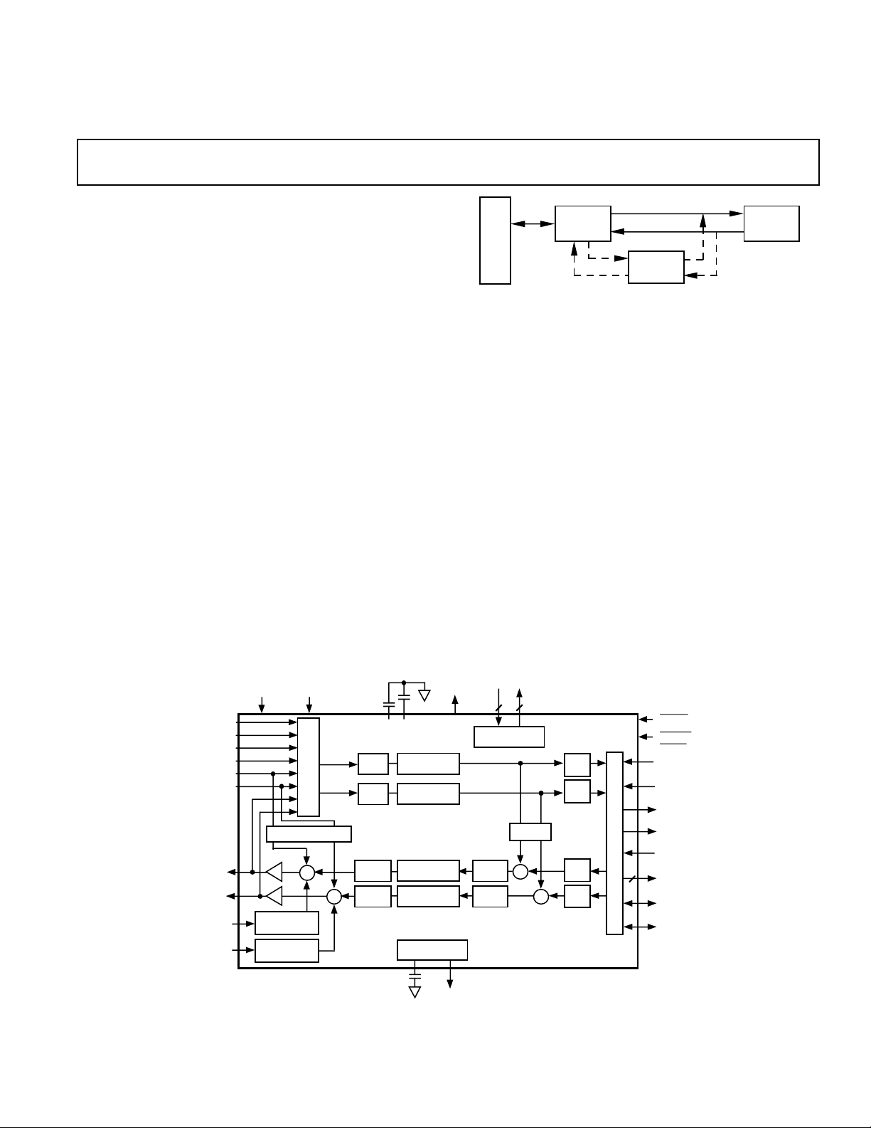
PRODUCT OVERVIEW
The AD1847 SoundPort® Stereo Codec integrates key audio
data conversion and control functions into a single integrated
circuit. The AD1847 is intended to provide a complete, low
cost, single-chip solution for business, game audio and multimedia applications requiring operation from a single +5 V supply. It provides a serial interface for implementation on a
computer motherboard, add-in or PCMCIA card. See Figure 1
for an example system diagram.
*Windows Sound System is a registered trademark of Microsoft Corp.
SoundPort is a registered trademark of Analog Devices, Inc.
FUNCTIONAL BLOCK DIAGRAM
ANALOG
I/O
LINE 1
INPUT
LINE 2
INPUT
AUX 1
INPUT
LINE
OUTPUT
AUX 2
INPUT
L
R
L
R
L
R
L
R
L
R
ANALOG
SUPPLY
DIGITAL
SUPPLY
M
U
X
GAIN/ATTEN/MUTE
L
∑
R
GAIN/ATTEN
/MUTE
GAIN/ATTEN
/MUTE
L
GAIN
R
GAIN
ATTEN/
MUTE
ATTEN/
∑
MUTE
∑∆ A/D
CONVERTER
∑∆ A/D
CONVERTER
∑∆ D/A
CONVERTER
∑∆ D/A
CONVERTER
REFERENCE
SoundPort Stereo Codec
AD1847
I
S
A
B
U
S
Figure 1. Example System Diagram
External circuit requirements are limited to a minimal number
of low cost support components. Anti-imaging DAC output
filters are incorporated on-chip. Dynamic range exceeds 70 dB
over the 20 kHz audio band. Sample rates from 5.5 kHz to
48 kHz are supported from external crystals.
The Codec includes a stereo pair of ∑∆ analog-to-digital converters (ADCs) and a stereo pair of ∑∆ digital-to-analog converters (DACs). Inputs to the ADC can be selected from four
stereo pairs of analog signals: line 1, line 2, auxiliary (“aux”)
line #1, and post-mixed DAC output. A software-controlled
programmable gain stage allows independent gain for each
channel going into the ADC. The ADCs’ output can be digitally
mixed with the DACs’ input.
The pair of 16-bit outputs from the ADCs is available over a serial interface that also supports 16-bit digital input to the DACs
and control/status information. The AD1847 can accept and
generate 16-bit twos-complement PCM linear digital data, 8-bit
unsigned magnitude PCM linear data, and 8-bit µ-law or A-law
companded digital data.
CLOCK
OUT
CRYSTALS
2 2
OSCILLATORS
ATTEN
ATTEN
∑
ATTEN
AD1847
ASIC AD1847
DSP
(Continued on page 7)
DIGITAL
I/O
RESET
POWER
2
DOWN
BUS
MASTER
TIME SLOT
INPUT
TIME SLOT
OUTPUT
SERIAL DATA
OUTPUT
SERIAL DATA
INPUT
EXTERNAL
CONTROL
SERIAL BIT
CLOCK
FRAME
SYNC
µ/A
LAW
S
µ/A
µ/A
µ/A
E
R
I
A
L
P
O
R
T
LAW
LAW
∑
LAW
REV. B
Information furnished by Analog Devices is believed to be accurate and
reliable. However, no responsibility is assumed by Analog Devices for its
use, nor for any infringements of patents or other rights of third parties
which may result from its use. No license is granted by implication or
otherwise under any patent or patent rights of Analog Devices.
2.25V
® Analog Devices, Inc., 1996
One Technology Way, P.O. Box 9106, Norwood, MA 02062-9106, U.S.A.
Tel: 617/329-4700 Fax: 617/326-8703
Page 2

AD1847–SPECIFICA TIONS
STANDARD TEST CONDITIONS UNLESS OTHERWISE NOTED
Temperature 25 °C DAC Output Conditions
Digital Supply (V
Analog Supply (V
Word Rate (F
Input Signal 1007 Hz No Output Load
Analog Output Passband 20 Hz to 20 kHz Mute Off
FFT Size 4096 ADC Input Conditions
V
IH
V
IL
V
OH
V
OL
ANALOG INPUT
Full-Scale Input Voltage (RMS Values Assume Sine Wave Input)
Line1, Line2, AUX1, AUX2 1 V rms
Input Impedance
Line1, Line2, AUX1, AUX2† 10 kΩ
Input Capacitance† 15 pF
) 5.0 V 0 dB Attenuation
DD
) 5.0 V Full-Scale Digital Inputs
CC
) 48 kHz 16-Bit Linear Mode
S
2.4 V 0 dB Gain
0.8 V –3.0 dB Relative to Full Scale
2.4 V Line Input
0.4 V 16-Bit Linear Mode
Min Typ Max Units
2.54 2.8 3.10 V p-p
PROGRAMMABLE GAIN AMPLIFIER—ADC
Min Typ Max Units
Step Size (All Steps Tested, –30 dB Input) 1.10 1.5 1.90 dB
PGA Gain Range Span† 21.0 24.0 dB
AUXILIARY INPUT ANALOG AMPLIFIERS/ATTENUATORS
Min Typ Max Units
Step Size (+12 dB to –28.5 dB, Referenced to DAC Full Scale) 1.3 1.5 1.7 dB
(–30 dB to –34.5 dB, Referenced to DAC Full Scale) 1.1 1.5 1.9 dB
Input Gain/Attenuation Range Span† 45.5 47.5 dB
AUX Input Impedance† 10 kΩ
DIGITAL DECIMATION AND INTERPOLATION FILTERS†
Min Max Units
Passband 0 0.4 3 F
S
Hz
Passband Ripple –0.1 +0.1 dB
Transition Band 0.4 3 F
Stopband 0.6 3 F
S
S
0.6 3 F
S
Hz
∞ Hz
Stopband Rejection 74 dB
Group Delay 30/F
S
Group Delay Variation Over Passband 0 µs
–2–
REV. B
Page 3

AD1847
ANALOG-TO-DIGITAL CONVERTERS
Min Typ Max Units
Resolution 16 Bits
Dynamic Range (–60 dB Input, THD+N Referenced to Full Scale, A-Weighted) 70 dB
THD+N (Referenced to Full Scale) 0.040 %
–68 dB
Signal-to-Intermodulation Distortion† 83 dB
ADC Crosstalk†
Line Inputs (Input L, Ground R, Read R; Input R, Ground L, Read L) –80 dB
Line1 to Line2 (Input Line1, Ground and Select Line2, Read Both Channels) –80 dB
Line to AUX1 –80 dB
Line to AUX2 –80 dB
Line to DAC –80 dB
Gain Error (Full-Scale Span Relative to V
Interchannel Gain Mismatch (Difference of Gain Errors) ±0.2 dB
DC Offset ±55 LSB
DIGITAL-TO-ANALOG CONVERTERS
Resolution 16 Bits
Dynamic Range (–60 dB Input, THD+N Referenced to Full Scale, A-Weighted) 76 dB
THD+N (Referenced to Full Scale) 0.025 %
Signal-to-Intermodulation Distortion† 86 dB
Gain Error (Full-Scale Span Relative to V
Interchannel Gain Mismatch (Difference of Gain Errors) ±0.2 dB
DAC Crosstalk† (Input L, Zero R, Measure R_OUT; Input R, Zero L, Measure L_OUT) –80 dB
Total Out-of-Band Energy† (Measured from 0.6 3 F
Audible Out-of-Band Energy (Measured from 0.6 3 FS to 22 kHz, Tested at FS = 5.5 kHz) –55 dB
DAC ATTENUATOR
Step Size (0 dB to –22.5 dB) (Tested at Steps 0 dB, –19.5) 1.3 1.5 1.7 dB
Step Size (–24 dB to –94 dB) 1.0 1.5 2.0 dB
Output Attenuation Range Span† –93 95 dB
DIGITAL MIX ATTENUATOR
Step Size (0 dB to –22.5 dB) (Tested at Steps 0 dB, –19.5) 1.3 1.5 1.7 dB
Step Size (–24 dB to –94 dB) 1.0 1.5 2.0 dB
Output Attenuation Range Span† –93.5 95.5 dB
ANALOG OUTPUT
Full-Scale Line Output Voltage 0.707 V rms
V
= 2.35* 1.80 2 2.20 V p-p
REFI
Line Output Impedance† 600 Ω
External Load Impedance 10 kΩ
Output Capacitance† 15 pF
External Load Capacitance 100 pF
V
(Clock Running) 2.00 2.50 V
REF
V
Current Drive 100 µA
REF
V
REFI
Mute Attenuation of 0 dB –80 dB
Fundamental† (LOUT)
Mute Click† 8mV
(|Muted Output Minus Unmuted
Midscale DAC Output|)
*Full-scale line output voltage scales with V
†Guaranteed, Not Tested.
REF
(e.g., V
REV. B
) ±10 %
REFI
Min Typ Max Units
–72 dB
) ±10 %
REFI
to 100 kHz) –50 dB
S
Min Typ Max Units
Min Typ Max Units
Min Typ Max Units
2.35 V
(typ) – 2.0 V 3 (V
OUT
REF
/2.35)).
–3–
Page 4

AD1847
SYSTEM SPECIFICATIONS
Min Typ Max Units
System Frequency Response† ±0.3 dB
(Line In to Line Out, 20 Hz to 20 kHz)
Differential Nonlinearity† ±1/2 Bit
Phase Linearity Deviation† 1 Degrees
STATIC DIGITAL SPECIFICATIONS
Min Max Units
High Level Input Voltage (VIH)
Digital Inputs 2.0 V
XTAL1/2I 2.4 V
Low Level Input Voltage (V
High Level Output Voltage (V
Low Level Output Voltage (V
Input Leakage Current (GO/NOGO Tested) –10 +10 µA
Output Leakage Current (GO/NOGO Tested) –10 +10 µA
TIMING PARAMETERS (Guaranteed Over Operating Temperature Range)
) 0.8 V
IL
) IOH = 1 mA 2.4 V
OH
) IOL = 4 mA 0.4 V
OL
DD
Min Typ Max Units
V
Serial Frame Sync Period (t
Clock to Frame Sync [SDFS] Propagation Delay (t
Data Input Setup Time (t
Data Input Hold Time (t
Clock to Output Data Valid (t
Clock to Output Three-State [High-Z] (t
Clock to Time Slot Output [TSO] Propagation Delay (t
RESET and PWRDOWN Lo Pulse Width (t
POWER SUPPLY
) 1/0.5 F
1
)15 ns
S
)15 ns
H
) 25 ns
DV
)20ns
HZ
RPWL
)20ns
PD1
)20ns
PD2
) 100 ns
S
µs
Min Max Units
Power Supply Range – Digital & Analog 4.75 5.25 V
Power Supply Current – Operating (10 kΩ Line Out Load) 140 mA
Analog Supply Current – Operating (10 kΩ Line Out Load) 70 mA
Digital Supply Current – Operating (10 kΩ Line Out Load) 70 mA
Analog Power Supply Current – Power Down 400 µA
Digital Power Supply Current – Power Down 400 µA
Power Dissipation – Operating (Current 3 Nominal Supply) 750 mW
Power Dissipation – Power Down (Current 3 Nominal Supply) 4 mW
Power Supply Rejection (@ 1 kHz)†
(At Both Analog and Digital Supply Pins, ADCs) 45 dB
(At Both Analog and Digital Supply Pins, DACs) 55 dB
CLOCK SPECIFICATIONS†
Min Max Units
Input Clock Frequency 27 MHz
Recommended Clock Duty Cycle ±10 %
Initialization/Sample Rate Change Time
16.9344 MHz Crystal Selected at Power-Up 171 ms
24.576 MHz Crystal Selected at Power-Up 171 ms
16.9344 MHz Crystal Selected Subsequently 6 ms
24.576 MHz Crystal Selected Subsequently 6 ms
†Guaranteed, not tested.
Specifications subject to change without notice.
–4–
REV. B
Page 5
AD1847
WARNING!
ESD SENSITIVE DEVICE
44 SDFS
43 SDO
42 SDI
41 GNDD
40 V
DD
39 SCLK
38 CLKOUT
37 XTAL2O
36 XTAL2I
35 XTAL1O
34 XTAL1I
33
32
31
30
29
28
27
26
25
24
23
PIN 1 IDENTIFIER
R_LINE1
V
REF
V
REFI
GNDA
V
CC
PWRDOWN
RESET
GNDD
V
DD
TSI
TSO
1
2
3
4
5
6
7
8
9
11
10
V
DD
GNDD
XCTL1
XCTL0
GNDD
V
DD
BM
L_AUX2
R_AUX2
L_OUT
N/C
R_LINE2 12
RFILT 13
GNDA 14
LFILT 15
L_LINE2 16
L_LINE1 17
GNDA 18
L_AUX1 20
R_AUX1 21
R_OUT 22
V
CC
19
Top View
(Not to Scale)
AD1847JST
N/C = NO CONNECT
ABSOLUTE MAXIMUM RATINGS*
Min Max Units
Power Supplies
Digital (V
Analog (V
) –0.3 6.0 V
DD
) –0.3 6.0 V
CC
Input Current
(Except Supply Pins) ±10.0 mA
Model Range Description Option*
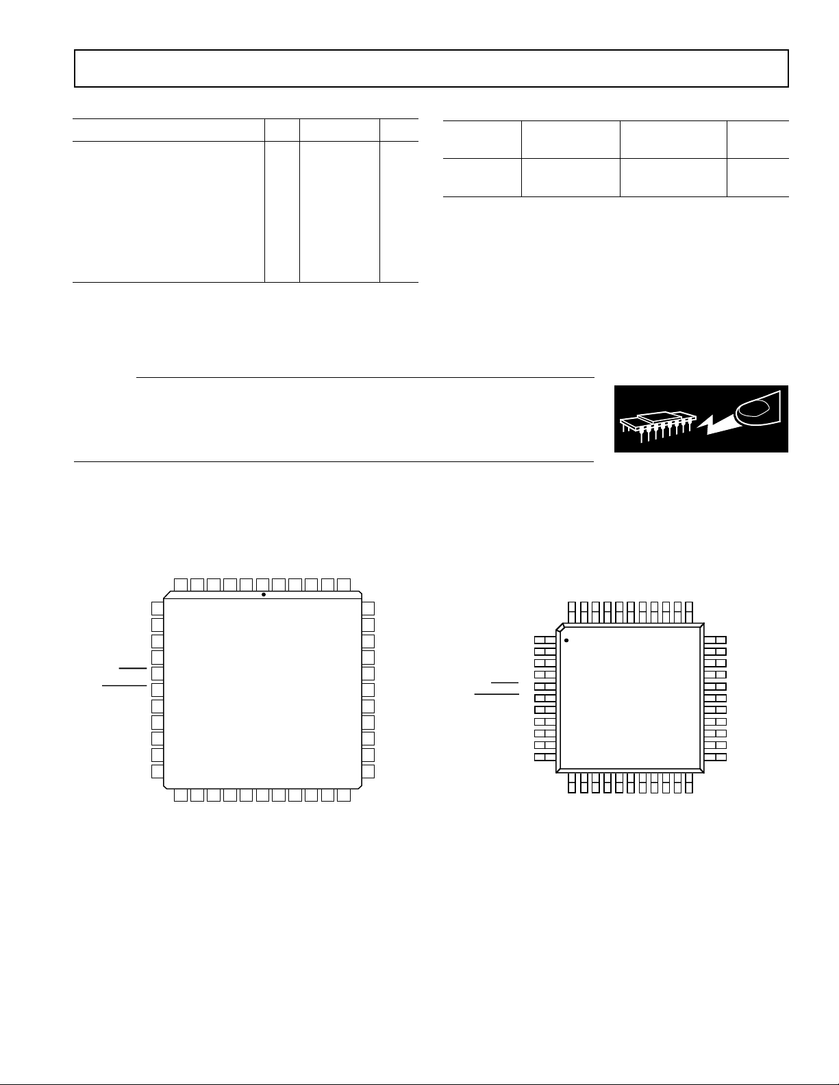
AD1847JP 0 °C to +70°C 44-Lead PLCC P-44A
AD1847JST 0°C to +70°C 44-Lead TQFP ST-44
*P = PLCC; ST = TQFP.
ORDERING GUIDE
Temperature Package Package
Analog Input Voltage (Signal Pins) –0.3 (VA+) + 0.3 V
Digital Input Voltage (Signal Pins) –0.3 (VD+) + 0.3 V
Ambient Temperature (Operating) 0 +70 °C
Storage Temperature –65 +150 °C
*Stresses greater than those listed under “Absolute Maximum Ratings” may cause
permanent damage to the device. This is a stress rating only and functional
operation of the device at these or any other conditions above those indicated in
the operational section of this specification is not implied. Exposure to absolute
maximum rating conditions for extended periods may affect device reliability.
CAUTION
ESD (electrostatic discharge) sensitive device. Electrostatic charges as high as 4000 V readily
accumulate on the human body and test equipment and can discharge without detection.
Although the AD1847 features proprietary ESD protection circuitry, permanent damage may
occur on devices subjected to high energy electrostatic discharges. Therefore, proper ESD
precautions are recommended to avoid performance degradation or loss of functionality.
PINOUTS
44-Lead PLCC 44-Lead TQFP
DD
SCLK
23
L_LINE1
XTAL2O
CLKOUT
4412645
43
25 28
CC
V
GNDA
XTAL2I
26
L_AUX1
XTAL1O
27
R_AUX1
XTAL1I
404142
R_OUT
39
38
37
36
35
34
33
32
31
30
29
V
DD
GNDD
XCTL1
XCTL0
GNDD
V
DD
BM
L_AUX2
R_AUX2
L_OUT
N/C
SDI
GNDD
3
AD1847JP
Top View
(Not to Scale)
21 24
22182019
LFILT
GNDA
V
L_LINE2
SDFS
SDO
7
TSO
8
TSI
V
9
DD
GNDD
10
11
RESET
V
CC
GNDA
V
REFI
V
REF
R_LINE1
12
13
14
15
16
17
N/C = NO CONNECT
R_LINE2
RFILT
PWRDOWN
REV. B
–5–
Page 6

AD1847
PIN DESCRIPTIONS
Parallel Interface
Pin Name PLCC TQFP I/O Description
SCLK 1 39 I/O Serial Clock. SCLK is a bidirectional signal that supplies the clock as an output to the
serial bus when the Bus Master (BM) pin is driven HI and accepts the clock as an input
when the BM pin is driven LO. The serial clock output is fixed at 12.288 MHz when
XTAL1 is selected, and 11.2896 MHz when XTAL2 is selected. SCLK runs continuously. An AD1847 should always be configured as the serial bus master unless it is a slave
in a daisy-chained multiple codec system.
SDFS 6 44 I/O Serial Data Frame Sync. SDFS is a bidirectional signal that supplies the frame synchroni-
zation signal as an output to the serial bus when the Bus Master (BM) pin is driven HI
and accepts the frame synchronization signal as an input when the BM pin is driven LO.
The SDFS frequency powers up at one half of the AD1847 sample rate (i.e., FRS bit = 0)
with two samples per frame and can be programmed to match the sample rate (i.e., FRS
bit = 1) with one sample per frame. An AD1847 should always be configured as the serial
bus master unless it is a slave in a daisy-chained multiple codec system.
SDI 4 42 I Serial Data Input. SDI is used by peripheral devices such as the host CPU or a DSP to
supply control and playback data information to the AD1847. All control and playback
transfers are 16 bits long, MSB first.
SDO 5 43 O Serial Data Output. SDO is used to supply status/index readback and capture data infor-
mation to peripheral devices such as the host CPU or a DSP. All status/index readback
and capture data transfers are 16 bits long, MSB first. Three-state output driver.
RESET 11 5 I Reset. The RESET signal is active LO. The assertion of this signal will initialize the
on-chip registers to their default values. See the “Control Register Definitions” section for
a description of the contents of the control registers after
PWRDOWN 12 6 I Powerdown. The PWRDOWN signal is active LO. The assertion of this signal will reset
the on-chip control registers (identically to the
AD1847 in a low power consumption mode. V
BM 33 27 I Bus Master. The assertion (HI) of this signal indicates that the AD1847 is the serial bus
master. The AD1847 will then supply the serial clock (SCLK) and the frame sync (SDFS)
signals for the serial bus. One and only one AD1847 should always be configured as the
serial bus master. If BM is connected to logic LO, the AD1847 is configured as a bus
slave, and will accept the SCLK and SDFS signals as inputs. An AD1847 should only be
configured as a serial bus slave when an AD1847 serial bus master already exists, in
daisy-chained multiple codec systems.
TSO 7 1 O Time Slot Output. This signal is asserted HI by the AD1847 coincidentally with the LSB
of the last time slot used by the AD1847. Used in daisy-chained multiple codec systems.
TSI 8 2 I Time Slot Input. The assertion of this signal indicates that the AD1847 should immedi-
ately use the next three time slots (TSSEL = 1) or the next six time slots (TSSEL = 0)
and then activate the TSO pin to enable the next device down the TDM chain. TSI
should be driven LO when the AD1847 is the bus master or in single codec systems. Used
in daisy-chained multiple codec systems.
CLKOUT 44 38 O Clock Output. This signal is the buffered version of the crystal clock output and the fre-
quency is dependent on which crystal is selected. This pin can be three-stated by driving
the BM pin LO or by programming the CLKTS bit in the Pin Control Register. See the
“Control Registers” section for more details. The CLKOUT frequency is 12.288 MHz
when XTAL1 is selected and 16.9344 MHz when XTAL2 is selected.
RESET signal) and will also place the
REF
RESET is deasserted.
and all analog circuitry are disabled.
Analog Signals
Pin Name PLCC TQFP I/O Description
L_LINE1 23 17 I Left Line Input #1. Line level input for the #1 left channel.
R_LINE1 17 11 I Right Line Input #1. Line level input for the #1 right channel.
L_LINE2 22 16 I Left Line Input #2. Line level input for the #2 left channel.
R_LINE2 18 12 I Right Line Input #2. Line level input for the #2 right channel.
L_AUX1 26 20 I Left Auxiliary Input #1. Line level input for the AUX1 left channel.
R_AUX1 27 21 I Right Auxiliary Input #1. Line level input for the AUX1 right channel.
L_AUX2 32 26 I Left Auxiliary Input #2. Line level input for the AUX2 left channel.
R_AUX2 31 25 I Right Auxiliary Input #2. Line level input for the AUX2 right channel.
L_OUT 30 24 O Left Line Output. Line level output for the left channel.
R_OUT 28 22 O Right Line Output. Line level output for the right channel.
–6–
REV. B
Page 7

AD1847
Miscellaneous
Pin Name PLCC TQFP I/O Description
XTAL1I 40 34 I 24.576 MHz Crystal #1 Input.
XTAL1O 41 35 O 24.576 MHz Crystal #1 Output.
XTAL2I 42 36 I 16.9344 MHz Crystal #2 Input.
XTAL2O 43 37 O 16.9344 MHz Crystal #2 Output.
XCTL1:O 37 & 36 31 & 30 O External Control. These TTL signals reflect the current status of register bits inside the
AD1847. They can be used for signaling or to control external logic.
V
REF
V
REFI
L_FILT 21 15 I Left Channel Filter Capacitor. This pin requires a 1.0 µF capacitor to analog ground
R_FILT 19 13 I Right Channel Filter Capacitor. This pin requires a 1.0 µF capacitor to analog ground
NC 29 23 No Connect. Do not connect.
Power Supplies
Pin Name PLCC TQFP I/O Description
16 10 O Voltage Reference. Nominal 2.25 volt reference available externally as a voltage datum
for dc-coupling and level-shifting. V
should not have any signal dependent load.
REF
15 9 I Voltage Reference Internal. Voltage reference filter point for external bypassing only.
for proper operation.
for proper operation.
V
CC
13 & 25 7 & 19 I Analog Supply Voltage (+5 V).
GNDA 14, 20, 24 8, 14, 18 I Analog Ground.
V
DD
2, 9, 34, 39 40, 3, 28, 33 I Digital Supply Voltage (+5 V).
GNDD 3, 10, 35, 38 41, 4, 29, 32 I Digital Ground.
(Continued from page 1)
The ∑∆ DACs are preceded by a digital interpolation filter. An
attenuator provides independent user volume control over each
DAC channel. Nyquist images are removed from the DACs’
analog stereo output by on-chip switched-capacitor and
continuous-time filters. Two stereo pairs of auxiliary line-level
inputs can also be mixed in the analog domain with the DAC
output.
The AD1847 serial data interface uses a Time Division Multiplex (TDM) scheme that is compatible with DSP serial ports
configured in Multi-Channel Mode with 32 16-bit time slots
(i.e., SPORT0 on the ADSP-2101, ADSP-2115, etc.).
Analog Mixing
AUX1 and AUX2 analog stereo signals can be mixed in the analog domain with the DAC output. Each channel of each auxiliary analog input can be independently gained/attenuated from
+12 dB to –34.5 dB in –1.5 dB steps or completely muted. The
post-mixed DAC output is available on L_OUT and R_OUT
externally and as an input to the ADCs.
Even if the AD1847 is not playing back data from its DACs, the
analog mix function can still be active.
Analog-to-Digital Datapath
The ∑∆ ADCs incorporate a proprietary fourth-order modulator. A single pole of passive filtering is all that is required for
antialiasing the analog input because of the ADC’s high 64
AUDIO FUNCTIONAL DESCRIPTION
This section overviews the functionality of the AD1847 and is
intended as a general introduction to the capabilities of the device. As much as possible, detailed reference information has
been placed in “Control Registers” and other sections. The user
is not expected to refer repeatedly to this section.
Analog Inputs
The AD1847 SoundPort Stereo Codec accepts stereo line-level
inputs. All inputs should be capacitively coupled (ac-coupled) to
the AD1847. LINE1, LINE2, and AUX1, and post-mixed DAC
output analog stereo signals are multiplexed to the internal programmable gain amplifier (PGA) stage.
The PGA following the input multiplexer allows independent
selectable gains for each channel from 0 to 22.5 dB in +1.5 dB
steps. The Codec can operate either in a global stereo mode or
in a global mono mode with left-channel inputs appearing at
times oversampling ratio. The ADCs include digital decimation
filters that low-pass filter the input to 0.4 3 F
word rate or “sampling frequency.”) ADC input overrange conditions will cause status bits to be set that can be read.
Digital-to-Analog Datapath
The ∑∆ DACs contain a programmable attenuator and a lowpass digital interpolation filter. The anti-imaging interpolation
filter oversamples and digitally filters the higher frequency images. The attenuator allows independent control of each DAC
channel from 0 dB to –94.5 dB in 1.5 dB steps plus full mute.
The DACs’ ∑∆ noise shapers also oversample and convert the
signal to a single-bit stream. The DAC outputs are then filtered
in the analog domain by a combination of switched-capacitor
and continuous-time filters. These filters remove the very high
frequency components of the DAC bitstream output. No external components are required.
both channel outputs.
. (“FS’’ is the
S
REV. B
–7–
Page 8
AD1847
EXPANSION
DAC INPUT
MSB LSB
15 0
MSB
15 0
MSB
15 0
COMPRESSED
INPUT DATA
LSB
3/2 2/1
LSB
3/2 2/1
0 0 0 / 0 0
87
TRUNCATION
COMPRESSION
MSB LSB
15 0
MSB
LSB
15 0
MSB
LSB
15 0
3/2 2/1
ADC OUTPUT
0 0 0 0 0 0 0 0
87
Changes in DAC output attenuation take effect only on zero
crossings of the digital signal, thereby eliminating “zipper” noise
on playback. Each channel has its own independent zero-crossing
detector and attenuator change control circuitry. A timer guarantees that requested volume changes will occur even in the absence of an input signal that changes sign. The time-out period
is 8 milliseconds at a 48 kHz sampling rate and 48 milliseconds
at an 8 kHz sampling rate. (Time-out [ms] ≈ 384/F
[kHz]).
S
Digital Mixing
Stereo digital output from the ADCs can be mixed digitally with
the input to the DACs. Digital output from the ADCs going out
of the serial data port is unaffected by the digital mix. Along the
digital mix datapath, the 16-bit linear output from the ADCs is
attenuated by an amount specified with control bits. Both channels of the monitor data are attenuated by the same amount.
(Note that internally the AD1847 always works with 16-bit
PCM linear data, digital mixing included; format conversions
take place at the input and output.)
Sixty-four steps of –1.5 dB attenuation are supported to
–94.5 dB. The digital mix datapath can also be completely
muted, preventing any mixing of the digital input with the digital output. Note that the level of the mixed signal is also a function of the input PGA settings, since they affect the ADCs’
output.
The attenuated digital mix data is digitally summed with the
DAC input data prior to the DACs’ datapath attenuators. The
digital sum of digital mix data and DAC input data is clipped at
plus or minus full scale and does not wrap around. Because
both stereo signals are mixed before the output attenuators, mix
data is attenuated a second time by the DACs’ datapath
attenuators.
Analog Outputs
A stereo line-level output is available at external pins. Other
output types such as headphone and speaker must be implemented in external circuitry. The stereo line-level outputs
should be capacitively coupled (ac-coupled) to the external circuitry. Each channel of this output can be independently
muted. When muted, the outputs will settle to a dc value near
V
, the midscale reference voltage.
REF
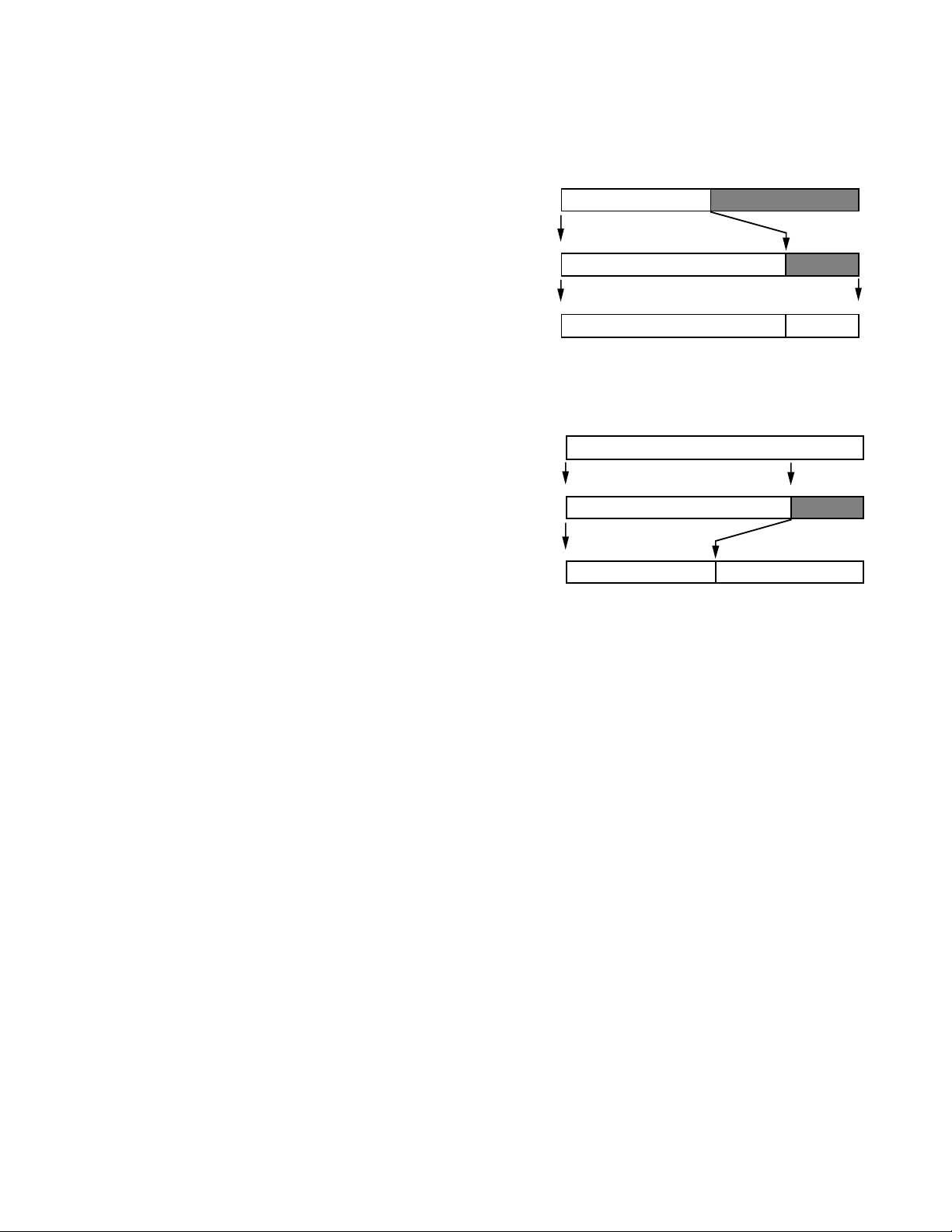
Digital Data Types
The AD1847 supports four global data types: 16-bit twoscomplement linear PCM, 8-bit unsigned linear PCM,
companded µ-law, and 8-bit companded A-law, as specified by
control register bits. Eight-bit data is always left-justified in 16bit fields; in other words, the MSBs of all data types are always
aligned; in yet other words, full-scale representations in all four
formats correspond to equivalent full-scale signals. The eight
least significant bit positions of 8-bit data in 16-bit fields are ignored on digital input and zoned on digital output (i.e., truncated).
The 16-bit PCM data format is capable of representing 96 dB of
dynamic range. Eight-bit PCM can represent 48 dB of dynamic
range. Companded µ-law and A-law data formats use nonlinear
coding with less precision for large-amplitude signals. The loss
of precision is compensated for by an increase in dynamic range
to 64 dB and 72 dB, respectively.
On input, 8-bit companded data is expanded to an internal linear representation, according to whether µ-law or A-law was
specified in the Codec’s internal registers. Note that when µ-law
compressed data is expanded to a linear format, it requires 14
bits. A-law data expanded requires 13 bits.
Figure 2. A-Law or µ-Law Expansion
When 8-bit companding is specified, the ADCs’ linear output is
compressed to the format specified.
Figure 3. A-Law or µ-Law Compression
Note that all format conversions take place at input or output.
Internally, the AD1847 always uses 16-bit linear PCM representations to maintain maximum precision.
Power Supplies and Voltage Reference
The AD1847 operates from +5 V power supplies. Independent
analog and digital supplies are recommended for optimal performance though excellent results can be obtained in single-supply
systems. A voltage reference is included on the Codec and its
2.25 V buffered output is available on an external pin (V
REF
).
The reference output can be used for biasing op amps used in
dc coupling. The internal reference must be externally bypassed
to analog ground at the V
pin, and must not be used to bias
REFI
external circuitry.
Clocks and Sample Rates
The AD1847 operates from two external crystals, XTAL1 and
XTAL2. The two crystal inputs are provided to generate a wide
range of sample rates. The oscillators for these crystals are on
the AD1847, as is a multiplexer for selecting between them.
They can be overdriven with external clocks by the user, if so
desired. At a minimum, XTAL1 must be provided since it is selected as the reset default. If XTAL2 is not used, the XTAL2
input pin should be connected to ground. The recommended
crystal frequencies are 16.9344 MHz and 24.576 MHz. From
them, the following sample rates can be selected: 5.5125, 6.615,
8, 9.6, 11.025, 16, 18.9, 22.05, 27.42857, 32, 33.075, 37.8,
44.1, 48 kHz.
–8–
REV. B
Page 9

AD1847
CONTROL REGISTERS
Control Register Mapping
The AD1847 has six 16-bit and thirteen 8-bit on-chip useraccessible control registers. Control information is sent to the
AD1847 in the 16-bit Control Word. Status information is sent
from the AD1847 in the 16-bit Status Word. Playback Data and
Capture Data each have two 16-bit registers for the right and
left channels. Additional 8-bit Index Registers are accessed via
indirect addressing in the AD1847 Control Word. [Index Registers are reached with indirect addressing.] The contents of an
indirect addressed Index Register may be readback by the host
CPU or DSP (during the Status Word/Index Readback time
slot) by setting the Read Request (RREQ) bit in the Control
Word. Note that each 16-bit register is assigned its own time
slot, so that the AD1847 always consumes six 16-bit time slots.
Figure 4 shows the mapping of the Control Word, Status Word/
Index Readback and Data registers to time slots when TSSEL = 0.
TSSEL = 0 is used when the SDI and SDO pins are tied together (i.e., “1-wire” system). This configuration is efficient in
terms of component interconnect (one bidirectional wire for serial data input and output), but inefficient in terms of time slot
usage (six slots consumed on single bidirectional Time Division
Multiplexed [TDM] serial bus). When TSSEL = 0, serial data
input to the AD1847 occurs sequentially with serial data output
from the AD1847 (i.e., Control Word, Left Playback and Right
Playback data is received on the SDI pin, then the Status Word/
lndex Readback, Left Capture and Right Capture data is transmitted on the SDO pin).
Slot Register Name (16-Bit)
0 Control Word Input
1 Left Playback Data Input
2 Right Playback Data Input
3 Status Word/Index Readback Output
4 Left Capture Data Output
5 Right Capture Data Output
Figure 4. Control Register Mapping with TSSEL = 0
Figure 5 shows the mapping of the Control Word, Status Word/
Index Readback and Data registers to time slots when TSSEL =
1. Note that the six 16-bit registers “share” three time slots.
TSSEL = 1 is used when the SDI and SDO pins are independent inputs and output (i.e., “2-wire” system). This configuration is inefficient in terms of component interconnect (two
unidirectional wires for serial data input and output), but efficient in terms of time slot usage (three slots consumed on each
of two unidirectional TDM serial buses). When TSSEL = 1, serial data input to the AD1847 occurs concurrently with serial
data output from the AD1847 (i.e., Control Word reception on
the SDI pin occurs simultaneously with Status Word/lndex
Readback transmission on the SDO pin).
Slot Register Name (16-Bit)
0 Control Word Input
1 Left Playback Data Input
2 Right Playback Data Input
0 Status Word/Index Readback Output
1 Left Capture Data Output
2 Right Capture Data Output
Figure 5. Control Register Mapping with TSSEL = 1
An Index Register readback request to an invalid index address
(11, 14 and 15) will return the contents of the Status Word. Attempts to write to an invalid index address (11, 14 and 15) will
have no effect on the AD1847. As mentioned above, the RREQ
bit of the Control Word is used to request Status Word output
or Index Register readback output during either time slot 3
(TSSEL = 0) or time slot 0 (TSSEL = 1). RREQ is set for Index Register readback output, and reset for Status Word output.
When Index Register readback is requested, the Index Readback
bit format is the same as the Control Word bit format. All status
bits are updated by the AD1847 before a new Control Word is
received (i.e., at frame boundaries). Thus, if TSSEL = 0 and
the Control Word written at slot 0 causes some status bits to
change, the change will show up in the Status Word transmitted
at slot 3 of the same sample.
REV. B
–9–
Page 10

AD1847
Control Word (16-Bit)
Data 15 Data 14 Data 13 Data 12 Data 11 Data 10 Data 9 Data 8
CLOR MCE RREQ r es I A3 IA 2 IA1 IA 0
Data 7 Data 6 Data 5 Data 4 Data 3 Data 2 Data 1 Data 0
DATA7 DATA6 DATA5 DATA4 DATA3 DATA2 DATA1 DATA0
DATA7:0 Index Register Data. These bits are the data for the desired AD1847 Index Register referenced by the Index Address.
Written by the host CPU or DSP to the AD1847.
IA3:0 Index Register Address. These bits define the indirect address of the desired AD1847 Index Register. Written by the host
CPU or DSP to the AD1847.
RREQ Read Request. Setting this bit indicates that the current transfer is a request by the host CPU or DSP for readback of the
contents of the indirect addressed Index Register. When this bit is set (RREQ = HI), the AD1847 will not transmit its
Status Word in the following Status Word Index readback slot, but will instead transmit the data in the Index Register
specified by the Index Address. Although the Index Readback is transmitted in the following Status Word/Index
Readback time slot, the format of the Control Word is used (i.e., CLOR, MCE, RREQ and the Index Register Address
in the most significant byte, and the readback Index Register Data in the least significant byte). When this bit is reset
(RREQ = LO), the AD1847 will transmit its Status Word in the following Status Word Index Readback time slot.
A read request is serviced in the next available Index Readback time slot. If TSSEL = 0, the Index Register readback
data is transmitted in slot 3 of the same sample. If TSSEL = 1, Index Register readback data is transmitted in slot 0 of
the next sample. If TSSEL changes from 0 to 1, Index Register readback will occur twice, in slot 3 of the current sample,
and slot 0 of the next. If TSSEL changes from 1 to 0, the last read request is lost.
res Reserved for future expansion. Write zeros (LO) to all reserved bits.
MCE Mode Change Enable. This bit must be set (MCE = HI) whenever protected control register bits of the AD1847 are
changed. The Data Format register, the Miscellaneous Information register, and the ACAL bit of the Interface Configu-
ration register can NOT be changed unless this bit is set. The DAC outputs will be muted when MCE is set. The user
must mute the AUX1 and AUX2 channels when this bit is set (no audio activity should occur). Written by the host CPU
or DSP to the AD1847. This bit is HI after reset.
CLOR Clear Overrange. When this bit is set (CLOR = HI), the overrange bits in the Status Word are updated every sample.
When this bit is reset (CLOR = LO), the overrange bits in the Status Word will record the largest overrange value. The
largest overrange value is sticky until the CLOR bit is set. Written by the host CPU or DSP to the AD1847. Since there
can be up to 2 samples in the data pipeline, a change to CLOR may take up to 2 samples periods to take effect. This bit
is HI after reset.
Immediately after reset, the contents of this register is: 1100 0000 0000 0000 (C000h).
Left/Right Playback/Capture Data (16-Bit)
The data formats for Left Playback, Right Playback, Left Capture and Right Capture are all identical.
Data 15 Data 14 Data 13 Data 12 Data 11 Data 10 Data 9 Data 8
DATA15 DATA14 DATA13 DATA12 DATA11 DATA10 DATA9 DATA8
Data 7 Data 6 Data 5 Data 4 Data 3 Data 2 Data 1 Data 0
DATA7 DATA6 DATA5 DATA4 DATA3 DATA2 DATA1 DATA0
DATA15:0 Data Bits. These registers contain the 16-bit, MSB first data for capture and playback. The host CPU or DSP reads the
capture data from the AD1847. The host CPU or DSP writes the playback data to the AD1847. For 8-bit linear or 8-bit
companded modes, only DATA15:8 contain valid data; DATA7:0 are ignored during capture, and are zeroed during
playback. Mono mode plays back the same audio sample on both left and right channels. Mono capture only captures
data from the left audio channel. See “Serial Data Format” Timing Diagram.
Immediately after reset, the content of these registers is: 0000 0000 0000 0000 (0000h).
–10–
REV. B
Page 11

AD1847
Status Word (16-Bit)
Data 15 Data 14 Data 13 Data 12 Data 11 Data 10 Data 9 Data 8
re s r es RREQ res ID 3 I D2 ID1 I D 0
Data 7 Data 6 Data 5 Data 4 Data 3 Data 2 Data 1 Data 0
res res ORR1 ORR0 ORL1 ORL0 ACI INIT
INIT Initialization. This bit is an indication to the host that frame syncs will stop and the serial bus will be shut down. INIT is
set HI on the last valid frame. It is reset LO for all other frames. Read by the host CPU or DSP from the AD1847.
The INIT bit is set HI on the last sample before the serial interface is inactivated. The only condition under which the
INIT bit is set is when a different sample rate is programmed. If FRS = 0 (32 slots per frame, two samples per frame)
and the sample rate is changed in the first sample of the 32 slot frame (i.e., during slots 0 through 15), the INIT bit will
be set on the second sample of that frame (i.e., during slots 16 through 31). If FRS = 0 and the sample rate is changed in
the second sample of the 32 slot frame, the INIT bit will be set on the second sample of the following frame.
ACI Autocalibrate In-Progress. This bit indicates that autocalibration is in progress or the Mode Change Enable (MCE) state
has been recently exited. When exiting the MCE state with the ACAL bit set, the ACI bit will be set HI for 384 sample
periods. When exiting the MCE state with the ACAL bit reset, the ACAL bit will be set HI for 128 sample periods, indicating that offset and filter values are being restored. Read by the host CPU or DSP from the AD1847.
0 Autocalibration not in progress
1 Autocalibration is in progress
ACI clear (i.e., reset or LO) should be recognized by first polling for a HI on the sample after the MCE bit is reset, and
then polling for a LO. Note that it is important not to start polling until one sample after MCE is reset, because if MCE
is set while ACI is HI, an ACI LO on the following sample will suggest a false clear of ACI.
ORL1:0 Overrange Left Detect. These bits indicate the overrange on the left input channel. Read by the host CPU or DSP from
the AD1847.
0 Greater than –1.0 dB underrange
1 Between –1.0 dB and 0 dB underrange
2 Between 0 dB and 1.0 dB overrange
3 Greater than 1.0 dB overrange
ORR1:0 Overrange Right Detect. These bits indicate the overrange on the right input channel. Read by the host CPU or DSP
from the AD1847.
0 Greater than –1.0 dB underrange
1 Between –1.0 dB and 0 dB underrange
2 Between 0 dB and 1.0 dB overrange
3 Greater than 1.0 dB overrange
ID3:0 AD1847 Revision ID. These four bits define the revision level of the AD1847. The first version of the AD1847 is desig-
nated ID = 0001. Read by the host CPU or DSP from the AD1847.
RREQ This bit is reset LO for the Status Word, echoing the RREQ state written by the host CPU or DSP in the previous Con-
trol Word. Read by the host CPU or DSP from the AD1847.
res Reserved for future expansion. All reserved bits read zero (LO).
Immediately after reset, the contents of this register is: 0000 0001 0000 0000 (0100h).
REV. B
–11–
Page 12

AD1847
Index Readback (16-Bit)
Data 15 Data 14 Data 13 Data 12 Data 11 Data 10 Data 9 Data 8
CLOR MCE RREQ r es I A3 IA 2 IA1 IA 0
Data 7 Data 6 Data 5 Data 4 Data 3 Data 2 Data 1 Data 0
DATA7 DATA6 DATA5 DATA4 DATA3 DATA2 DATA1 DATA0
DATA7:0 Index Register Data. These bits are the readback data from the desired AD1847 Index Register referenced by the Index
Address from the previous Control Word (with the RREQ bit set). Read by the host CPU or DSP from the AD1847.
IA3:0 Index Register Address. These bits echo the indirect address (written during the previous Control Word (with the RREQ
bit set) of the desired AD1847 Index Register to be readback. Read by the host CPU or DSP from the AD1847.
RREQ Read Request. This bit is set HI for Index Readback, echoing the RREQ state written by the host CPU or DSP in the
previous Control Word. Read by the host CPU or DSP from the AD1847.
res Reserved for future expansion. All reserved bits read zero (LO).
MCE Mode Change Enable. This bit echoes the MCE state written by the host CPU or DSP during the previous* Control
Word (with the RREQ bit set). Read by the host CPU or DSP from the AD1847.
CLOR Clear Overrange. This bit echoes the CLOR state written by the host CPU or DSP during the previous Control Word
(with the RREQ bit set). Read by the host CPU or DSP from the AD1847.
Immediately after reset, the contents of this register is: 1110 0000 0000 0000 (E000h).
Indirect Mapped Registers
Following in Figure 6 is a table defining the mapping of AD1847 8-bit Index Registers to Index Address. These registers are accessed
by writing the appropriate 4-bit Index Address in the Control Word.
Index Register Name
0 Left Input Control
1 Right Input Control
2 Left Aux #1 Input Control
3 Right Aux #l Input Control
4 Left Aux #2 Input Control
5 Right Aux #2 Input Control
6 Left DAC Control
7 Right DAC Control
8 Data Format
9 Interface Configuration
10 Pin Control
1 1 Invalid Address
12 Miscellaneous Information
1 3 Digital Mix Control
1 4 Invalid Address
1 5 Invalid Address
Figure 6. Index Register Mapping
A detailed description of each of the Index Registers is given below.
–12–
REV. B
Page 13

AD1847
Left Input Control Register (Index Address 0)
IA3:0 Data 7 Data 6 Data 5 Data 4 Data 3 Data 2 Data 1 Data 0
0000 LSS1 LSS0 res res LIG3 LIG2 LIG1 LIG0
LIG3:0 Left Input Gain Select. The least significant bit of this 16-level gain select represents +1.5 dB. Maximum gain is
+22.5 dB.
res Reserved for future expansion. Write zeros (LO) to all reserved bits.
LSS1:0 Left Input Source Select. These bits select the input source for the left gain stage preceding the left ADC.
0 Left Line 1 Source Selected
1 Left Auxiliary 1 Source Selected
2 Left Line 2 Source Selected
3 Left Line 1 Post-Mixed Output Loopback Source Selected
This register’s initial state after reset is: 0000 0000 (00h).
Right Input Control Register (Index Address 1)
IA3:0 Data 7 Data 6 Data 5 Data 4 Data 3 Data 2 Data 1 Data 0
0001 RSS1 RSS0 re s re s R IG3 R IG2 R IG1 R IG0
RIG3:0 Right Input Gain Select. The least significant bit of this 16-level gain select represents +1.5 dB. Maximum gain is
+22.5 dB.
res Reserved for future expansion. Write zeros (LO) to all reserved bits.
RSS1:0 Right Input Source Select. These bits select the input source for the right gain stage preceding the right ADC.
0 Right Line 1 Source Selected
1 Right Auxiliary 1 Source Selected
2 Right Line 2 Source Selected
3 Right Line 1 Post-Mixed Output Loopback Source Selected
This register’s initial state after reset is: 0000 0000 (00h).
Left Auxiliary #1 Input Control Register (Index Address 2)
IA3:0 Data 7 Data 6 Data 5 Data 4 Data 3 Data 2 Data 1 Data 0
0010 LMX1 res res LX1G4 LX1G3 LX1G2 LX1G1 LX1G0
LX1G4:0 Left Auxiliary Input #1 Gain Select. The least significant bit of this 32-level gain/attenuate select represents –1.5 dB.
LX1G4:0 = 0 produces a +12 dB gain. LX1G4:0 = “01000” (8 decimal) produces 0 dB gain. Maximum attenuation is
–34.5 dB. Gains referred to 2.0 V p-p full-scale output level.
res Reserved for future expansion. Write zeros (LO) to all reserved bits.
LMX1 Left Auxiliary #1 Mute. This bit, when set HI, will mute the left channel of the Auxiliary #1 input source. This bit is set
HI after reset.
This register’s initial state after reset is: 1000 0000 (80h).
Right Auxiliary #1 Input Control Register (Index Address 3)
IA3:0 Data 7 Data 6 Data 5 Data 4 Data 3 Data 2 Data 1 Data 0
0011 RMX1 res res RX1G4 RX1G3 RX1G2 RX1G1 RX1G0
RX1G4:0 Right Auxiliary Input #1 Gain Select. The least significant bit of this 32-level gain/attenuate select represents –1.5 dB.
RX1G4:0 = 0 produces a +12 dB gain. RX1G4:0 = “01000” (8 decimal) produces 0 dB gain. Maximum attenuation is
–34.5 dB. Gains referred to 2.0 V p-p full-scale output level.
res Reserved for future expansion. Write zeros (LO) to all reserved bits.
RMX1 Right Auxiliary #1 Mute. This bit, when set to HI, will mute the right channel of the Auxiliary #1 input source. This bit is
set to HI after reset.
This register’s initial state after reset is: 1000 0000 (80h).
REV. B
–13–
Page 14

AD1847
Left Auxiliary #2 Input Control Register (Index Address 4)
IA3:0 Data 7 Data 6 Data 5 Data 4 Data 3 Data 2 Data 1 Data 0
0100 LMX2 res res LX2G4 LX2G3 LX2G2 LX2G1 LX2G0
LX2G4:0 Left Auxiliary #2 Gain Select. The least significant bit of this 32-level gain/attenuate select represents –1.5 dB.
LX2G4:0 = 0 produces a +12 dB gain. LX2G4:0 = “01000” (8 decimal) produces 0 dB gain. Maximum attenuation is
–34.5 dB. Gains referred to 2.0 V p-p full-scale output level.
res Reserved for future expansion. Write zeros (LO) to all reserved bits.
LMX2 Left Auxiliary #2 Mute. This bit, when set HI, will mute the left channel of the Auxiliary #2 input source. This bit is HI
after reset.
This register’s initial state after reset is: 1000 0000 (80h).
Right Auxiliary #2 Input Control Register (Index Address 5)
IA3:0 Data 7 Data 6 Data 5 Data 4 Data 3 Data 2 Data 1 Data 0
0101 RMX2 res res RX2G4 RX2G3 RX2G2 RX2G1 RX2G0
RX2G4:0 Right Auxiliary #2 Gain Select. The least significant bit of this 32-level gain/attenuate select represents –1.5 dB.
RX2G4:0 = 0 produces a +12 dB gain. RX2G4:0 = “01000” (8 decimal) produces 0 dB gain. Maximum attenuation is
–34.5 dB. Gains referred to 2.0 V p-p full-scale output level.
res Reserved for future expansion. Write zeros (LO) to all reserved bits.
RMX2 Right Auxiliary #2 Mute. This bit, when set HI, will mute the right channel of the Auxiliary #2 input source. This bit is
HI after reset.
This register’s initial state after reset is: 1000 0000 (80h).
Left DAC Control Register (Index Address 6)
IA3:0 Data 7 Data 6 Data 5 Data 4 Data 3 Data 2 Data 1 Data 0
0110 LDM res LDA5 LDA4 LDA3 LDA2 LDA1 LDA0
LDA5:0 Left DAC Attenuate Select. The least significant bit of this 64-level attenuate select represents –1.5 dB. LDA5:0 = 0 pro-
duces a 0 dB attenuation. Maximum attenuation is –94.5 dB.
res Reserved for future expansion. Write zeros (LO) to all reserved bits.
LDM Left DAC Mute. This bit, when set HI, will mute the left channel output. Auxiliary inputs are muted independently with
the Left Auxiliary Input Control Registers. This bit is HI after reset.
This register’s initial state after reset is: 1000 0000 (80h).
Right DAC Control Register (Index Address 7)
IA3:0 Data 7 Data 6 Data 5 Data 4 Data 3 Data 2 Data 1 Data 0
0111 RDM res RDA5 RDA4 RDA3 RDA2 RDA1 RDA0
RDA5:0 Right DAC Attenuate Select. The least significant bit of this 64-level attenuate select represents –1.5 dB. RDA5:0 = 0
produces a 0 dB attenuation. Maximum attenuation must be at least –94.5 dB.
res Reserved for future expansion. Write zeros (LO) to all reserved bits.
RDM Right DAC Mute. This bit, when set HI, will mute the right DAC output. Auxiliary inputs are muted independently with
the Right Auxiliary Input Control Registers. This bit is HI after reset.
This register’s initial state after reset is: 1000 0000 (80h).
–14–
REV. B
Page 15

AD1847
Data Format Register (Index Address 8)
IA3:0 Data 7 Data 6 Data 5 Data 4 Data 3 Data 2 Data 1 Data 0
1000 res FMT C/L S/M CFS2 CFS1 CFS0 CSL
The contents of this register can NOT be changed except when the AD1847 is in the Mode Change Enable (MCE) state (i.e., the MCE bit in
the Control Word is HI). Write attempts to this register when the AD1847 is not in the MCE state will not be successful.
CSL Clock Source Select. This bit selects the clock source to be used for the audio sample rate.
0 XTAL1 (24.576 MHz)
1 XTAL2 (16.9344 MHz)
CFS2:0 Clock Frequency Divide Select. These bits select the audio sample rate frequency. The audio sample rate depends on
which clock source is selected and the frequency of the clock source.
Divide XTAL1 XTAL2
CFS2:0 Factor 24.576 MHz 16.9344 MHz
0 3072 8.0 kHz 5.5125 kHz
1 1536 16.0 kHz 11.025 kHz
2 896 27.42857 kHz 18.9 kHz
3 768 32.0 kHz 22.05 kHz
4 448 Not Supported 37.8 kHz
5 384 Not Supported 44.1 kHz
6 512 48.0 kHz 33.075 kHz
7 2560 9.6 kHz 6.615 kHz
Note that the AD1847’s internal oscillators can be overdriven by external clock sources at the crystal inputs. This is the
configuration used by serial bus slave codecs in daisy-chained multiple codec systems. If an external clock source is applied, it will be divided down by the selected Divide Factor. The external clock need not be at the recommended crystal
frequencies.
S/M Stereo/Mono Select. This bit determines how the audio data streams are formatted. Selecting stereo will result with alter-
nating samples representing left and right audio channels. Mono playback plays the same audio sample on both channels.
Mono capture only captures data from the left audio channel.
0 Mono
1 Stereo
C/L Companded/Linear Select. This bit selects between a linear digital representation of the audio signal or a nonlinear, com-
panded format for all input and output data. The type of linear PCM or the type of companded format is defined by the
FMT bits.
0 Linear PCM
1 Companded
FMT Format Select. This bit defines the format for all digital audio input and output based on the state of the C/L bit.
Linear PCM (C/L = 0) Companded (C/L = 1)
0 8-bit unsigned linear PCM 8-bit µ-law companded
1 16-bit signed linear PCM 8-bit A-law companded
res Reserved for future expansion. Write zeros (LO) to all reserved bits.
This register’s initial state after reset is: 0000 0000 (00h).
REV. B
–15–
Page 16

AD1847
Interface Configuration Register (Index Address 9)
IA3:0 Data 7 Data 6 Data 5 Data 4 Data 3 Data 2 Data 1 Data 0
1001 res res res res ACAL res re s P E N
PEN Playback Enable. This bit will enable the playback of data in the format selected. PEN may be set and reset without
setting the MCE bit.
0 Playback Disabled
1 Playback Enabled
ACAL Autocalibrate Enable. This bit determines whether the AD1847 performs an autocalibrate when exiting from the Mode
Change Enable (MCE) state. If the ACAL bit is not set, the previous autocalibration values are used when returning from
the Mode Change Enable (MCE) state and no autocalibration takes place. Autocalibration must be preformed after initial
power-up for proper operation. This bit is HI after reset.
0 No autocalibration
1 Autocalibration allowed
NOTE: The ACAL bit can only be changed when the AD1847 is in the Mode Change Enable (MCE) state.
res Reserved for future expansion. Write zeros (LO) to all reserved bits.
This register’s initial state after reset is: 0000 1000 (08h).
Pin Control Register (Index Address 10)
IA3:0 Data 7 Data 6 Data 5 Data 4 Data 3 Data 2 Data 1 Data 0
1010 XCTL1 XCTL0 CLKTS res res res res res
CLKTS Clock Three-State. If the BM bit is HI, and the CLKTS bit is HI, then the CLKOUT pin will be three-stated. If the BM
bit is HI, and the bit CLKTS is LO, then the CLKOUT pin is not three-stated. If the BM bit is LO, then the CLKOUT
pin is always three-stated.
XCTL1:0 External Control. The state of these independent bits is reflected on the respective XCTL1 and XCTL0 pins of the
AD1847.
0 TTL logic LO on XCTL1, XCTL0 pins
1 TTL logic HI on XCTL1, XCTL0 pins
res Reserved for future expansion. Write zeros (LO) to all reserved bits.
This register’s initial state after reset is: 0000 0000 (00h).
Invalid Address (Index Address 11)
IA3:0 Data 7 Data 6 Data 5 Data 4 Data 3 Data 2 Data 1 Data 0
1011 inval inval inval inval inval inval inval inval
inval Writes to this index address are ignored. Index readback of this index address will return the Status Word.
–16–
REV. B
Page 17

AD1847
Miscellaneous Information Register (Index Address 12)
IA3:0 Data 7 Data 6 Data 5 Data 4 Data 3 Data 2 Data 1 Data 0
1100 FRS TSSEL res res res res res res
The Miscellaneous Information Register can only be changed when the AD1847 is in the Mode Change Enable (MCE) state. Changes to this
register are updated at the next Serial Data Frame Sync (SDFS) boundary. If FRS is LO (i.e., 32 slots per frame), and either TSSEL or FRS
change in the first sample of a frame, the change is not updated at the second sample of the same frame, but at the first sample of the next frame.
TSSEL Transmit Slot Select. This bit determines which TDM time slots the AD1847 should transmit on.
0 Transmit on time slots 3, 4 and 5. Used when SDI and SDO are tied together (i.e., “1-wire” system).
1 Transmit on slots 0, 1 and 2. Used when SDI and SDO are independent inputs and outputs
(i.e., “2-wire” system).
FRS Frame Size. This bit selects the number of time slots per frame.
0 Selects 32 slots per frame (two samples per frame sync or frame sync at half the sample rate).
1 Selects 16 slots per frame (one sample per frame sync or frame sync at the sample rate).
res Reserved for future expansion. Write zeros (LO) to all reserved bits.
This register’s initial state after reset is: 0000 0000 (00h).
Digital Mix Control Register (Index Address 13)
IA3:0 Data 7 Data 6 Data 5 Data 4 Data 3 Data 2 Data 1 Data 0
1101 DMA5 DMA4 DMA3 DMA2 DMA1 DMA0 res DME
DME Digital Mix Enable. This bit enables the digital mix of the ADCs’ output with the DACs’ input. When enabled, the data
from the ADCs is digitally mixed with other data being delivered to the DACs (regardless of whether or not playback
[PEN] is enabled, i.e., set). If there is a capture overrun, then the last sample captured before overrun will be used for
the digital mix. If playback is enabled (PEN set) and there is a playback underrun, then a midscale zero will be added to
the digital mix data.
0 Digital mix disabled (muted)
1 Digital mix enabled
DMA5:0 Digital Mix Attenuation. These bits determine the attenuation of the ADC output data mixed with the DAC input data.
The least significant bit of this 64-level attenuate select represents –1.5 dB. Maximum attenuation is –94.5 dB.
res Reserved for future expansion. Write zeros (LO) to all reserved bits.
This register’s initial state after reset is: 0000 0000 (00h).
Invalid Address (Index Address 14)
IA3:0 Data 7 Data 6 Data 5 Data 4 Data 3 Data 2 Data 1 Data 0
1110 inval inval inval inval inval inval inval inval
inval Writes to this index address are ignored. Index readback of this index address will return the Status Word.
Invalid Address (Index Address 15)
IA3:0 Data 7 Data 6 Data 5 Data 4 Data 3 Data 2 Data 1 Data 0
1111 inval inval inval inval inval inval inval inval
inval Writes to this index address are ignored. Index readback of this index address will return the Status Word.
REV. B
–17–
Page 18

AD1847
Serial Data Interface
The AD1847 serial data interface uses a Time Division Multiplex (TDM) scheme that is compatible with DSP serial ports
configured in Multi-Channel Mode with either 32 or 16 16-bit
time slots. An AD1847 is always the serial bus master, transmitting the serial clock (SCLK) and the serial data frame sync
(SDFS). The AD1847 always receives control and playback
data in time slots 0, 1 and 2. The AD1847 will transmit status
or index register readback and capture data in time slots 0, 1
and 2 if TSSEL = 1, and will transmit status or index register
readback and capture data in time slots 3, 4 and 5 if TSSEL =
0. The following table in Figure 7 shows an example of how the
time slots might be assigned.
In this example design, which uses the ADSP-21xx DSP, each
frame is divided into 32 time slots of 16-bits each (FRS = 0).
Two audio samples are contained in the 32 time slots, with a
single frame sync (SDFS) at the beginning of the frame. The
ADSP-21xx serial port (SPORT0) supports 32 time slots. The
format of the first 16 time slots (sample N) is the same as the
format of the second 16 time slots (sample N+1). In this example, 24 time slots are used, as indicated below. Note that
time slots 12 through 15 and 28 through 31 are unused in this
example, and that Figure 7 presumes that TSSEL = 0 (“1-wire”
system).
Slot Number Source Destination Format
0, 16 AD1847 Control Word
1, 17 ASIC AD1847 Left Playback Data
2, 18 Right Playback Data
3, 19 AD1847 Status Word/
Index Readback
4, 20 AD1847 ASIC Left Capture Data
5, 21 Right Capture Data
0, 16 AD1847 Control Word
1, 17 DSP AD1847 Left Playback Data
2, 18 Right Playback Data
3, 19 AD1847 Status Word/
Index Readback
4, 20 AD1847 DSP Left Capture Data
5, 21 Right Capture Data
6, 22 DSP Control
7, 23 ASIC D SP Left Processed
Playback Data
8, 24 Right Processed
Playback Data
9, 25 DSP Status
10, 26 D SP ASIC Left Processed
Capture Data
11, 27 Right Processed
Capture Data
Note that in this “1-wire” system example, the Digital Signal
Processor (DSP) and ISA Bus Interface ASIC (ASIC) use the
same slots to communicate to the AD1847. This reduces the
number of total time slots required and eliminates the need for
the AD1847 to distinguish between DSP data and ASIC data.
Also, in this example the ASIC and the DSP do not send data to
the AD1847 at the same time, so separate slots are unnecessary.
The digital data in the serial interface is pipelined up to 2
samples deep. This pipelining is required to properly resolve the
interface between the relatively fast fixed SCLK rate, and the
relatively slow sample rates (and therefore frame sync rates) at
which the AD1847 is capable of running. At low sample rates,
two samples of data can be serviced in a fraction of a sample period. For example, at an 8 kHz sample rate, 32 time slots only
consume 32 × 16 × (1/12.288 MHz) = 41.67 µs out of a 125 µs
period. The two-deep data pipeline thus allows sample overrun
(capture) and sample underrun (playback) to be avoided.
Figure 8 represents a logical view of the slot utilization between
devices.
SDI
SDO
3, 4, 5,
19, 20, 21
AD1847
9, 10, 11,
25, 26, 27
0, 1, 2, 16, 17, 18
ASIC
3, 4, 5, 19, 20, 21
0, 1, 2,
16, 17, 18
6, 7, 8,
22, 23, 24
NOTE: DSP MUST HAVE TWO SERIAL PORTS
ADSP-21XX
DR
DT
DT
DR
Figure 8. Time Slot Allocation Example
Note that this is a system specific 1-wire example. For non-DSP
operation, the DSP is either not present or disabled. If the DSP
is present, the ASIC configures the DSP through slot 6 (and slot
22) to three-state its outputs in time slots 0, 1 and 2 (and slots
16, 17 and 18). The ASIC can then enable its drivers for time
slots 0, 1 and 2 (and slots 16, 17 and 18). For DSP operation,
the ASIC three-states its outputs for time slots 0, 1 and 2 (and
slots 16, 17 and 18) and enables the DSP drivers for slots 0, 1
and 2 (and slots 16, 17, and 18).
An application note is available from Analog Devices with additional information on interfacing to the AD1847 serial port.
This application note can be obtained through your local Analog Devices representative, or downloaded from the DSP Bulletin Board Service at (617) 461-4258 (8 data bits, no parity, 1
stop bit, 300/1200/2400/4600 baud).
Figure 7. Time Slot Assignment Example
–18–
REV. B
Page 19

Control Word
Left Playback Data
Right Playback Data
AD1847
Data 15 Data 14 Data 13 Data 12 Data 11 Data 10 Data 9 Data 8
CLOR MCE RREQ re s IA3 IA 2 I A 1 IA 0
Data 7 Data 6 Data 5 Data 4 Data 3 Data 2 Data 1 Data 0
DATA7 DATA6 DATA5 DATA4 DATA3 DATA2 DATA1 DATA0
Data 15 Data 14 Data 13 Data 12 Data 11 Data 10 Data 9 Data 8
DATA15 DATA14 DATA13 DATA12 DATA11 DATA10 DATA9 DATA8
Data 7 Data 6 Data 5 Data 4 Data 3 Data 2 Data 1 Data 0
DATA7 DATA6 DATA5 DATA4 DATA3 DATA2 DATA1 DATA0
Data 15 Data 14 Data 13 Data 12 Data 11 Data 10 Data 9 Data 8
DATA15 DATA14 DATA13 DATA12 DATA11 DATA10 DATA9 DATA8
Data 7 Data 6 Data 5 Data 4 Data 3 Data 2 Data 1 Data 0
DATA7 DATA6 DATA5 DATA4 DATA3 DATA2 DATA1 DATA0
Status Word
Index Readback
Left Capture Data
Right Capture Data
Data 15 Data 14 Data 13 Data 12 Data 11 Data 10 Data 9 Data 8
re s re s RREQ r es ID3 I D 2 ID1 I D 0
Data 7 Data 6 Data 5 Data 4 Data 3 Data 2 Data 1 Data 0
res r es ORR1 ORR0 ORL1 ORL0 ACI INIT
Data 15 Data 14 Data 13 Data 12 Data 11 Data 10 Data 9 Data 8
CLOR MCE RREQ re s IA3 IA 2 I A 1 IA 0
Data 7 Data 6 Data 5 Data 4 Data 3 Data 2 Data 1 Data 0
DATA7 DATA6 DATA5 DATA4 DATA3 DATA2 DATA1 DATA0
Data 15 Data 14 Data 13 Data 12 Data 11 Data 10 Data 9 Data 8
DATA15 DATA14 DATA13 DATA12 DATA11 DATA10 DATA9 DATA8
Data 7 Data 6 Data 5 Data 4 Data 3 Data 2 Data 1 Data 0
DATA7 DATA6 DATA5 DATA4 DATA3 DATA2 DATA 1 DATA0
REV. B
Data 15 Data 14 Data 13 Data 12 Data 11 Data 10 Data 9 Data 8
DATA15 DATA14 DATA13 DATA12 DATA11 DATA10 DATA9 DATA8
Data 7 Data 6 Data 5 Data 4 Data 3 Data 2 Data 1 Data 0
DATA7 DATA6 DATA5 DATA4 DATA3 DATA2 DATA1 DATA0
–19–
Page 20

AD1847
IA3:0 Data 7 Data 6 Data 5 Data 4 Data 3 Data 2 Data 1 Data 0 Index
0000 LSS1 LSS0 res res LIG3 LIG2 LIG1 LIG0 0
0001 RSS1 RSS0 res res RIG3 RIG2 RIG1 RIG0 1
0010 LMX1 res res LX1G4 LX1G3 LX1G2 LX1G1 LX1G0 2
0011 RMX1 res re s RX1G4 RX1G3 RX1G2 RX1G1 RX1G0 3
0100 LMX2 res res LX2G4 LX2G3 LX2G2 LX2G1 LX2G0 4
0101 RMX2 res re s RX2G4 RX2G3 RX2G2 RX2G1 RX2G0 5
0110 LDM res LDA5 LDA4 LDA3 LDA2 LDA1 LDA0 6
0111 RDM res RDA5 RDA4 RDA3 RDA2 RDA1 RDA0 7
1000 res FMT C/L S/M CFS2 CFS1 CFS0 CSL 8
1001 res res res res ACAL r es re s PE N 9
1010 XCTL1 XCTL0 CLKTS re s res res res res 1 0
1011 inval inval inval inval inval inval inval inval 1 1
1100 FRS TSSEL res res res res res res 12
1101 DMA5 DMA4 DMA3 DMA2 DMA1 DMA0 res DME 1 3
1110 inval inval inval inval inval inval inval inval 1 4
1111 inval inval inval inval inval inval inval inval 1 5
Figure 9. Register Map Summary
Control Register Mapping Summary
A detailed map of the control register bit assignments is summarized for reference in Figure 9.
Daisy-Chained Multiple Codecs
Multiple AD1847s can be configured in a daisy-chain system
with a single master Codec and one or more slave Codecs.
Codecs in a daisy-chained configuration are synchronized at the
sample level.
The master and slave AD1847s should be powered-up together.
If this is not possible, the slave(s) should power-up before the
master Codec, such that the slave(s) are ready when the master
starts to drive the serial interface, and a serial data frame sync
(SDFS) can synchronize the master and slave(s).
The sample rate for the master and slave(s) should be programmed together. If this is not possible, the slave(s) should be
programmed before the master AD1847. A slave AD1847 enters
a time-out period after a new sample rate has been selected.
During this time-out period, a slave will ignore any activity on
the SDFS signal (i.e., frame syncs). There is no software means
to determine when a slave has exited from this time-out period
and is ready to respond to frame syncs. However, as long as the
AD1847 master is driving the serial interface, a frame sync will
not occur before the slave Codec(s) are ready.
Note that the time slots for all slave AD1847s must be assigned
to those slots which immediately follow the time slots consumed
by the master AD1847 so that the TSO (Time Slot Output)/TSI
(Time Slot Input) signaling operates properly. For example, in a
2-wire system with one master and one slave, the time slot assignment should be 0, 1, 2 (16, 17, 18) for the master AD1847,
and 3, 4, 5 (19, 20, 21) for the slave AD1847.
Figure 10 illustrates the connection between master and slave(s)
in a daisy-chained, multiple Codec system. Note that the TSI
pin of the master Codec should be tied to digital ground. The
XTAL1I pin of the slaves should be connected to digital
ground, and XTAL1O pin should be left unconnected, while
the XTAL2I pin should be connected to the CLKOUT pin of
the AD1847 master, and the XTAL2O pin generates a driven
version of the CLKOUT signal applied to the XTAL2I pin.
INITIALIZATION AND PROCEDURES
Reset and Power Down
A total reset of the AD1847 is defined as any event which
requires both the digital and analog section of the AD1847 to
return to a known and stable state. Total reset mode, as well as
power down, occurs when the
has been asserted low for minimum power consumption. When
the
PWRDOWN signal is deasserted, the AD1847 must be calibrated by setting the ACAL bit and exiting from the Mode
Change Enable (MCE) state.
The reset occurs, and only resets the digital section of the
AD1847, when the
serted LO to initialize all registers to known values. See the register definitions for the exact values initialized. The register reset
defaults include TSSEL = 0 (1-wire system) and FRS = 0
(32 slots per frame). If the target application requires a 2-wire
system design or 16 slots per frame, the AD1847 can be
bootstrapped into these configurations.
RESET pin of the AD1847 has been as-
PWRDOWN pin of the AD1847
–20–
REV. B
Page 21

AD1847
24.576
XTAL1I,O XTAL2I,O
SCLK
SDFS
SDI
SDO
SCLK
SDFS
SDI
SDO
SCLK
SDFS
SDI
SDO
16.9344
MHz
MHz
2
AD1847
(MASTER)
TSO CLKOUT
TSI XTAL2I
XTAL1O
XTAL2O
(SLAVE 1)
TSO XTAL1I
TSI XTAL2I
XTAL1O
XTAL2O
(SLAVE 2)
TSO XTAL1I
2
TSI
N/C
N/C
Figure 10a. One-Wire Daisy-Chained Codec Interconnect
24.576
XTAL1I, O XTAL2I, O
SCLK
SDFS
SDI
SDO
SCLK
SDFS
SDI
SDO
SCLK
SDFS
SDI
SDO
16.9344
MHz
MHz
2
AD1847
(MASTER)
TSO CLKOUT
TSI XTAL2I
XTAL1O
XTAL2O
(SLAVE 1)
TSO XTAL1I
TSI XTAL2I
XTAL1O
XTAL2O
(SLAVE 2)
TSO XTAL1I
2
TSI
N/C
N/C
Figure 10b. Two-Wire Daisy-Chained Codec Interconnect
To bootstrap into TSSEL = 1 (i.e., 2-wire system design), the
host CPU or DSP must transmit to the AD1847 in slot 0 a
Control Word with the MCE bit set HI, IA3:0 = “1100” to
address the Miscellaneous Information Index Register, and
DATA7:0 = “X100 000” to set the TSSEL bit HI. To bootstrap
into FRS = 1 (i.e., 16 slots per frame), the host CPU or DSP
must transmit to the AD1847 in slot 0 a Control Word with the
MCE bit set HI, IA3:0 = “1100” to address the Miscellaneous
Information Index Register, and DATA7:0 = “1X00 0000” to
set the FRS bit HI.
The host CPU or DSP must maintain the MCE bit set HI in
slot 16, which is the Control Word of the second sample of
the frame, so that the AD1847 does not initiate autocalibration
prematurely. At the next frame sync, the AD1847 will be
reconfigured.
The AD1847 must be reset after power up. When the
RESET
signal is deasserted, the AD1847 will autocalibrate when the
MCE bit is reset LO (i.e., when exiting the Mode Change Enable state) only if the ACAL bit is set. If the ACAL bit is not
set, the previous autocalibration values will be used.
The AD1847 will not function properly unless an autocalibration is performed after power up.
During power down, the serial port digital output pins and the
analog output pins take the following states:
SCLK–LO if BM is HI (i.e., bus master), input pin if BM is
LO (i.e., bus slave)
SDFS–LO if BM is HI, input pin if BM is LO
SDO–three-state
TSO–three-state
CLKOUT–LO if BM HI, three-state if BM is LO
V
–pulled to analog ground
REF
L_OUT, R_ OUT– pulled to analog ground
Clock Connections and Clock Rates
When the AD1847 is configured as a bus slave (BM = LO), the
XTAL1I pin should be connected to digital ground, and the
XTAL2I pin should be tied to the CLKOUT of the AD1847
bus master. The XTAL1O and the XTAL2O pins should be left
unconnected. When the AD1847 is configured as a bus master
(BM = HI), the XTAL1I and the XTAL1O pin should be connected to a 24.576 MHz crystal, and the XTAL2I and
XTAL2O pin should be connected to a 16.9344 MHz crystal.
When XTAL1 is selected (by resetting the CSL bit LO in the
Data Format Register) as the clock source, the SCLK pin will
generated a serial clock at 12.288 MHz (or one half of the crystal frequency applied at XTAL1), and the CLKOUT pin will
also generate a clock output at 12.288 MHz when the AD1847
is in bus master mode (BM = HI). When XTAL2 is selected (by
setting the CSL bit HI in the Data Format Register) as the clock
source, the SCLK pin will generate a serial clock at 11.2896 MHz
(or two thirds of the crystal frequency applied at XTAL2), and
the CLKOUT pin will generate a clock output at 16.9344 MHz
when the AD1847 is in bus master mode (BM = HI). The
CLKOUT pin will be three-stated when the AD1847 is placed
in bus slave mode (BM = LO).
When the selected frame size is 32 slots per frame (by resetting
the FRS bit LO in the Miscellaneous Information Register), the
SDFS pin will generate a serial data frame sync at the frequency
of the selected sample rate divided by two, when the AD1847 is
in bus master mode (BM = HI). When the selected frame size is
16 slots per frame (by setting the FRS bit HI in the Miscellaneous Information Register), the SDFS pin will generate a serial
data frame sync at the frequency of the selected sample rate,
when the AD1847 is in bus master mode (BM = HI).
REV. B
–21–
Page 22

AD1847
When the AD1847 is in bus slave mode (BM = LO), the TSI
pin should be connected to the TSO pin of the AD1847 master
or slave which has been assigned to the preceding time slots.
The signal on the TSO pin is essentially the signal received on
the TSI pin, but delayed by 3 or 6 time slots from TSI (depending on the state of TSSEL). The frequency of the transitions on
the TSI and TSO lines is equivalent to the frequency on the
SDFS pin.
When the AD1847 is in bus master mode (BM = HI), the TSI
pin should be connected to digital ground. The signal on the
TSO pin is essentially the same as the signal output on the
SDFS pin, but delayed by 3 or 6 time slots from SDFS (again,
depending on the state of TSSEL).
Mode Change Enable State
The AD1847 must be in the Mode Change Enable (MCE) state
before any changes to the ACAL bit of the Interface Configuration Register, the Data Format Register, or the Miscellaneous
Information Register are allowed. Note that the MCE bit does
not have to be reset LO in order for changes to take effect.
Digital Mix
Digital mix is enabled via the DME bit in the Digital Mix Control Register. The digital mix routes the digital data from the
ADCs to the DACs. The mix can be digitally attenuated via bits
also in the Digital Mix Control Register. The ADC data is
summed with the DAC data supplied at the digital bus interface. When digital mix is enabled and the PEN bit is not set,
ADC data is summed with zeros to produce the DAC output.
If the sum of the digital mix (ADC output and DAC input from
the serial bus interface) is greater than full scale, the AD1847
will send a positive or negative full scale value to the DACs,
whichever is appropriate (clipping).
Autocalibration
The AD1847 has the ability to calibrate its ADCs and DACs for
greater accuracy by minimizing dc offsets. Autocalibration occurs whenever the AD1847 exits from the Mode Change Enable
(MCE) state AND the ACAL bit in the Interface Configuration
Register has been set.
The completion of the autocalibration sequence can be determined by polling the Autocalibration In-Progress (ACI) bit in
the Status Word. This bit will be HI while the autocalibration is
in progress and LO once autocalibration has completed. The
autocalibration sequence will take at least 384 sample periods.
The autocalibration procedure is as follows:
1. Mute both left and right AUX1 and AUX2 inputs via the Left
Auxiliary Input and Right Auxiliary Input Control Registers.
2. Place the AD1847 in the Mode Change Enable (MCE) state
using the MCE bit of the AD1847 Control Word. Set the
ACAL bit in the Interface Configuration Register.
3. Exit from the Mode Change Enable state by resetting the
MCE bit.
4. Poll the ACI bit in the AD1847 Status Word for a HI
(autocalibration in progress), then poll the ACI bit for a LO
(autocalibration complete).
5. Unmute the AUX inputs, if used.
If ACAL is not set, the AD1847 is muted for 128 sample periods after resetting the MCE bit, and the ACI bit in the Status
Word is set HI during this 128 sample periods. Autocalibration
must be performed after power-up to ensure proper operation of
the AD1847.
Exiting from the MCE state always causes ACI to go HI. If the
ACAL bit is set when MCE state is exited, then the ACI bit will
be HI for 384 sample periods. If the ACAL bit is reset when
MCE is exited, then the ACI bit will be HI for 128 sample
periods.
Changing Sample Rates
The internal states of the AD1847 are synchronized by the
selected sample frequency defined in the Data Format Register.
The changing of either the clock source or the clock frequency
divide requires a special sequence for proper AD1847 operation.
1. Mute the outputs of the AD1847 and enter the Mode Change
Enable (MCE) state by setting the MCE bit of the AD1847
Control Word.
2. During a single atomic or nondivisible write cycle, change the
Clock Frequency Divide Select (CFS) and/or the Clock
Source Select (CSL) bits of the Data Format Register to the
desired values. CFS and CSL can be programmed in the
same Control Word as MCE.
3. The INIT bit in the Status Word will be set HI at the last
sample of the next frame to indicate that the serial port will be
disabled for a timeout period.
4. The AD1847 requires a period of time to resynchronize its
internal states to the newly selected clock. During this time,
the AD1847 will be unable to respond at its serial interface
port (i.e., no frame syncs will be generated). The time-out
period is 2
for subsequent changes of sample rate.
5. Exit the Mode Change Enable state by resetting the MCE bit.
Upon exiting the MCE state, an autocalibration of duration
384 sample periods or an output mute of duration 128 sample
periods occurs, depending on the state of the ACAL bit.
6. Poll the ACI bit in the AD1847 Status Word for a HI (indicating that autocalibration is in progress) then poll the ACI
bit for a LO (indicating that autocalibration has completed).
Once the ACI bit has been read back LO, normal operation of
the Codec can resume.
The CSL and CFS bits cannot be changed unless the AD1847
is in the Mode Change Enable state (i.e., the MCE bit in the
AD1847 Control Word is set). Attempts to change the contents
of the Data Format Register without MCE set will result in the
write cycle not being recognized (the bits will not be updated).
The MCE bit should not be reset until after the INIT bit in the
AD1847 Status Word is detected HI. After the INIT bit is detected HI, the serial port is disabled. When the next frame sync
arrives (after the time-out period), all internal clocks are stable
and the serial port is ready for normal operation.
21
3 SCLK ≈ 170 ms after power-up, and ≈ 5 ms
–22–
REV. B
Page 23

AD1847
DATA FORMAT DEFINITIONS
There are four data formats supported by the AD1847: 16-bit
signed, 8-bit unsigned, 8-bit companded µ-law, and 8-bit com-
panded A-law. The AD1847 supports these four formats because
each of them have found wide use in important applications.
16-Bit Signed Format
The 16-bit signed format (also called 16-bit twos-complement)
is the standard method of representing 16-bit digital audio. This
format yields 96 dB of dynamic range and is common in consumer compact disk audio players. This format uses the value
– 32768 (8000h) to represent minimum analog amplitude while
32767 (7FFFh) represents maximum analog amplitude. Intermediate values are a linear interpolation between minimum and
maximum amplitude values.
MAX
ANALOG VALUE
8-Bit Companded Formats
The 8-bit companded formats (µ-law and A-law) are used in the
telecommunications industry. Both of these formats are used in
ISDN communications and workstations; µ-law is the standard
for the United States and Japan while A-law is used in Europe.
Companded audio allows either 64 dB or 72 dB of dynamic
range using only 8-bits per sample. This is accomplished using a
nonlinear formula which assigns more digital codes to lower amplitude analog signals at the expense of resolution of higher amplitude signals. The µ-law format of the AD1847 conforms to
the Bell System µ = 255 companding law while the A-law format
conforms to CCITT “A” law models. Figure 13 shows approximately how both the µ-law and A-law companding schemes be-
have. Refer to the standards mentioned above for an exact
definition.
MAX
ANALOG VALUE
MIN
8000h
0000h 7FFFh
DIGITAL VALUE
Figure 11. 16-Bit Signed Format
8-Bit Unsigned Format
The 8-bit unsigned format is commonly used in the personal
computer industry. This format delivers 48 dB of dynamic
range. The value 0 (00h) is used to represent minimum analog
amplitude while 255 (FFh) is used to represent maximum analog amplitude. Intermediate values are a linear interpolation between minimum and maximum amplitude values. The least
significant byte of the 16-bit internal data is truncated to create
the 8-bit output samples.
MAX
ANALOG VALUE
MIN
00h
7Fh FFh
DIGITAL VALUE
MIN
00h
FFh 80h
DIGITAL VALUE
AAh
µ-law
A-lawD5h2Ah
Figure 13. 8-Bit Companded Format
APPLICATIONS CIRCUITS
The AD1847 Stereo Codec has been designed to require a minimum of external circuitry. The recommended circuits are shown
in Figures 14 through 22. Analog Devices estimates that the total cost of all the components shown in these Figures, including
crystals, to be less than $3 in 10,000 quantities.
Industry-standard compact disc “line-levels” are 2 V
centered
rms
around analog ground. (For other audio equipment, “line level”
is much more loosely defined.) The AD1847 SoundPort is a
+5 V only powered device. Line level voltage swings for the
AD1847 are defined to be 1 V
0.707 V
for a sine wave DAC output. Thus, 2 V
rms
for a sine wave ADC input and
rms
input ana-
rms
log signals must be attenuated and either centered around the
reference voltage intermediate between 0 V and +5 V or
ac-coupled. The V
pin will be at this intermediate voltage,
REF
nominally 2.25 V. It has limited drive but can be used as a voltage datum to an op amp input. Note, however, that dc-coupled
inputs are not recommended, as they provide no performance
benefits with the AD1847 architecture. Furthermore, dc offset
differences between multiple dc-coupled inputs create the potential for “clicks” when changing the input mux selection.
REV. B
Figure 12. 8-Bit Unsigned Format
–23–
Page 24

AD1847
47k
1µF
L_OUT
47k
1µF
R_OUT
SSM2135
20k
470µF
18k
V
REF
HEADPHONE
LEFT
20k
470µF
18k
HEADPHONE
RIGHT
L_OUT
R_OUT
1.0µF
LFILT
1.0µF
RFILT
Circuits for 2 V
line-level inputs and auxiliaries are shown in
rms
Figure 14 and Figure 15. Note that these are divide-by-two
resistive dividers. The input resistor and 560 pF (1000 pF)
capacitor provide the single-pole of antialias filtering required
for the ADCs. If line-level inputs are already at the 1 V
rms
levels
expected by the AD1847, the resistors in parallel with the
560 pF (1000 pF) capacitors can be omitted. If the application
does not route the AUX2 inputs to the ADCs, then no antialias
filtering is required (only the 1 µF ac coupling capacitor).
5.1k
5.1k
4.3k
0.33 µF
0.33 µF
1µF
L_LINE1
L_LINE2
R_LINE1
R_LINE2
L_AUX1
L_AUX2
Figure 14. 2 V
5.1k
560pF
NPO
5.1k
560pF
NPO
Line-Level Input Circuit for Line Inputs
rms
3.3k
1000pF
NPO
Figure 17 shows ac-coupled line outputs. The resistors are
used to center the output signals around analog ground. If
dc-coupling is desired, V
could be used with op amps as
REF
mentioned previously.
Figure 17. Line Output Connections
A circuit for headphone drive is illustrated in Figure 18. Drive is
supplied by +5 V operational amps. The circuit shown ac
couples the headphones to the line output.
4.3k
1µF
R_AUX1
R_AUX2
Figure 15. 2 V
3.3k
1000pF
NPO
Line-Level Input Circuit for AUX Inputs
rms
Figure 16 illustrates one example of how an electret condenser
microphone requiring phantom power could be connected to
the AD1847. V
is shown buffered by an op amp; a transistor
REF
like a 2N4124 will also work well for this purpose. Note that if a
battery-powered microphone is used, the buffer and R2s are not
needed. The values of R1, R2, and C should be chosen in light
of the mic characteristics and intended gain. Typical values for
these might be R1 = 20 kΩ, R2 = 2 kΩ, and C = 220 pF.
C
R1
1/2 SSM2135
1/2 SSM2135
OR AD820
C
R1
1/2 SSM2135
OR AD820
OR AD820
0.33µF
0.33µF
L_LINE1
L_LINE2
V
REF
R_LINE1
R_LINE2
V
REF
LEFT
ELECTRET
CONDENSER
MICROPHONE
INPUT
RIGHT
ELECTRET
CONDENSER
MICROPHONE
INPUT
R2
R2
1µF
1µF
5k
5k
Figure 18. Headphone Drive Connections
Figure 19 illustrates reference bypassing. V
should only be
REFI
connected to its bypass capacitors.
V
REFI
10µF
0.1µF
V
REF
10µF
Figure 19. Voltage Reference Bypassing
Figure 20 illustrates signal-path filtering capacitors, L_FILT
and R_FILT. The AD1847 must use 1.0 µF capacitors. The
1.0 µF capacitors required by the AD1847 can be of any type.
Figure 20. External Filter Capacitor Connections
Figure 16. “Phantom-Powered” Microphone Input Circuit
–24–
REV. B
Page 25

AD1847
The crystals shown in the crystal connection circuitry of Figure
21 should be fundamental-mode and parallel-tuned. Two
sources for the exact crystals specified are Component Marketing Services in Massachusetts, U.S. at 617/762-4339 and
Cardinal Components in New Jersey, U.S. at 201/746-0333.
Note that using the exact data sheet frequencies is not required
and that external clock sources can be used to overdrive the
AD1847s internal oscillators. (See the description of the CFS2:0
control bits above.) If using an external clock source, apply it to
the crystal input pins while leaving the crystal output pins unconnected. Attention should be paid to providing low-jitter external input clocks .
XTAL1I XTAL1O
20 64pF 20 64pF
24.576MHz
XTAL2I XTAL2O
20 64pF 20 64pF
16.9344MHz
Figure 21. Crystal Connections
Analog Devices also recommends a pull-down resistor on the
PWRDOWN signal.
Good, standard engineering practices should be applied for
power-supply decoupling. Decoupling capacitors should be
placed as close as possible to package pins. If a separate analog
power supply is not available, the circuit shown in Figure 22 is
recommended when using a single +5 V supply. Ferrite beads
suffice for the inductors shown. This circuitry should be as close
to the supply pins as is practical.
Analog Devices recommends a split ground plane as shown in
Figure 23. The analog plane and the digital plane are connected
directly under the AD1847. Splitting the ground plane directly
under the SoundPort Codec is optimal because analog pins will
be located directly above the analog ground plane and digital
pins will be located directly above the digital ground plane for
the best isolation. The digital and analog grounds should be tied
together in the vicinity of the AD1847. Other schemes may also
yield satisfactory results. If the split ground plane recommended
here is not possible, the AD1847 should be entirely over the
analog ground plane with the ASIC and DSP over the digital
plane.
DIGITAL
GROUND
PLANE
BM L_AUX2
AD1847
PWRDOWN
V
CC
ANALOG
GROUND
PLANE
Figure 23. Recommended Ground Plane
+5V SUPPLY
FERRITE
0.1µF
FERRITE
0.1µF
1µF
1µF
V
1µF
0.1µF
DD
0.1µF
0.1µF
V
DD
VCCV
0.1µF
V
DD
CC
0.1µF
V
DD
1.6
Figure 22. Recommended Power Supply Bypassing
REV. B
–25–
Page 26

AD1847
10
–120
–90
–110
–100
–60
–80
–70
–50
–30
–20
0
–10
–40
1.00.10.0 0.8 0.90.70.60.50.40.30.2
dB
SAMPLE FREQUENCY – F
S
FREQUENCY RESPONSE PLOTS
10
0
–10
–20
–30
–40
–50
dB
–60
–70
–80
–90
–100
–110
–120
0.0
0.1
SAMPLE FREQUENCY – F
0.8 0.90.70.60.50.40.30.2
S
Figure 24. AD1847 Analog-to-Digital Frequency Response
(Full-Scale Line-Level Inputs, 0 dB Gain)
1.0
Figure 26. AD1847 Digital-to-Analog Frequency Response
(Full-Scale Inputs, 0 dB Attenuation)
10
0
–10
–20
–30
–40
–50
dB
–60
–70
–80
–90
–100
–110
–120
0.40
SAMPLE FREQUENCY – F
0.64 0.680.600.560.520.480.44
S
Figure 25. AD1847 Analog-to-Digital Frequency Response
–Transition Band (Full-Scale Line-Level Inputs, 0 dB Gain)
0.70
Figure 27. AD1847 Digital-to-Analog Frequency Response
–Transition Band (Full-Scale Inputs, 0 dB Attenuation)
–26–
10
0
–10
–20
–30
–40
–50
dB
–60
–70
–80
–90
–100
–110
–120
SAMPLE FREQUENCY – F
S
0.700.40 0.64 0.680.600.560.520.480.44
REV. B
Page 27

SCLK
t
RPWL
RESET
PWRDOWN
16-BIT
STEREO
8-BIT
STEREO
SCLK
SDFS
16-BIT
MONO
8-BIT
MONO
CONTROL
LEFT
PB
SDI/
SDO
TIME
SLOT 0
TIME
SLOT 1
TIME
SLOT 2
CONTROL
STATUS
RIGHT
PLAYBACK
RIGHT
PLAYBACK
LEFT
PLAYBACK
LEFT
CAPTURE
CONTROL
STATUS
LEFT
CAPTURE
LEFT
PLAYBACK
LEFT
CAPTURE
SDI/
SDO
SDI/
SDO
0
LEFT
CAP
STATUS
RIGHT
PB
RIGHT
CAP
0
CONTROL
LEFT
PB
SDI/
SDO
0
LEFT
CAP
STATUS
LEFT
CAP
0
AD1847
SDFS
SDI
SDO
SCLK
SDFS
SDI or
SDO
TSO
t
t
PD1
S
BIT 15
BIT 15
t
H
BIT 14
t
DV
BIT 14
Figure 28. Time Slot Timing Diagram
t
PD1
15 3210151413
14 13
LAST VALID TIME SLOT
Figure 29. TSO Timing Diagram
BIT 0
t
HZ
BIT 0
t
Figure 30. Reset and Power Down Timing Diagram
PD2
Figure 31. Serial Data Format, 2-Wire System (TSSEL = 1)
TIME
SLOT 0
TIME
SLOT 1
TIME
SLOT 2
TIME
SLOT 3
TIME
SLOT 4
TIME
SLOT 5
SCLK
SDFS
16-BIT
SDI/
STEREO
SDO
16-BIT
SDI/
MONO
SDO
SDI/
8-BIT
STEREO
SDO
8-BIT
SDI/
MONO
SDO
Figure 32. Serial Data Format, 1-Wire System (TSSEL = 0)
CONTROL LEFT RIGHT STATUS LEFT RIGHT
CONTROL LEFT STATUS LEFT
CONTROL
CONTROL
LEFT
LEFT
RIGHT
STATUS
STATUS
LEFT RIGHT
LEFT
PLAYBACK
0
0
LEFT
CAPTURE
LEFT
0
0
REV. B
–27–
Page 28

AD1847
OUTLINE DIMENSIONS
Dimensions shown in inches and (mm).
44-Lead PLCC
(P-44A)
0.180 (4.57)
0.165 (4.19)
40 6
39
29
28
0.110 (2.79)
0.085 (2.16)
0.048 (1.21)
0.042 (1.07)
0.020
(0.50)
0.048 (1.21)
0.042 (1.07)
7
17
18
R
PIN 1
IDENTIFIER
TOP VIEW
0.656 (16.66)
0.650 (16.51)
0.695 (17.65)
0.685 (17.40)
0.056 (1.42)
0.042 (1.07)
SQ
SQ
44-Terminal Plastic Thin Quad Flatpack (TQFP)
(ST-44)
0.063 (1.60)
0.030 (0.75)
0.018 (0.45)
SEATING
PLANE
0.006 (0.15)
0.002 (0.05)
MAX
0.057 (1.45)
0.053 (1.35)
33
34
44
1
0.031 (0.80)
0.472 (12.00) SQ
TOP VIEW
(PINS DOWN)
BSC
0.018 (0.45)
0.012 (0.30)
23
22
12
11
0.025 (0.63)
0.015 (0.38)
0.021 (0.53)
0.013 (0.33)
0.63 (16.00)
0.59 (14.99)
0.032 (0.81)
0.026 (0.66)
0.050
(1.27)
BSC
0.040 (1.01)
0.025 (0.64)
0.394
(10.0)
SQ
INDEX PAGE
PRODUCT OVERVIEW . . . . . . . . . . . . . . . . . . . . . . . . 1
AD1847 SPECIFICATIONS . . . . . . . . . . . . . . . . . . . . . 2
ORDERING GUIDE . . . . . . . . . . . . . . . . . . . . . . . . . . . 5
PINOUTS . . . . . . . . . . . . . . . . . . . . . . . . . . . . . . . . . . . . 5
PIN DESCRIPTIONS . . . . . . . . . . . . . . . . . . . . . . . . . . . 6
AUDIO FUNCTIONAL DESCRIPTION . . . . . . . . . . . 7
Analog Inputs . . . . . . . . . . . . . . . . . . . . . . . . . . . . . . . . 7
Analog Mixing . . . . . . . . . . . . . . . . . . . . . . . . . . . . . . . 7
Analog-to-Digital Datapath . . . . . . . . . . . . . . . . . . . . . 7
Digital-to-Analog Datapath . . . . . . . . . . . . . . . . . . . . . 7
Digital Mixing . . . . . . . . . . . . . . . . . . . . . . . . . . . . . . . 8
Analog Outputs . . . . . . . . . . . . . . . . . . . . . . . . . . . . . . 8
Digital Data Types . . . . . . . . . . . . . . . . . . . . . . . . . . . . 8
Power Supplies and Voltage Reference . . . . . . . . . . . . . 8
Clocks and Sample Rates . . . . . . . . . . . . . . . . . . . . . . . 8
CONTROL REGISTERS . . . . . . . . . . . . . . . . . . . . . . . . 9
Control Register Mapping . . . . . . . . . . . . . . . . . . . . . . 9
Control Word . . . . . . . . . . . . . . . . . . . . . . . . . . . . . . . 10
Left/Right Playback/Capture Data . . . . . . . . . . . . . . . 10
Status Word . . . . . . . . . . . . . . . . . . . . . . . . . . . . . . .: 11
Index Readback . . . . . . . . . . . . . . . . . . . . . . . . . . . . . 12
Indirect Mapped Registers . . . . . . . . . . . . . . . . . . . . . 12
Left Input Control Register . . . . . . . . . . . . . . . . . . . . 13
Right Input Control Register . . . . . . . . . . . . . . . . . . . 13
Left Auxiliary #1 Input Control Register . . . . . . . . . . 13
Right Auxiliary #1 Input Control Register . . . . . . . . . 13
Left Auxiliary #2 Input Control Register . . . . . . . . . . 14
Right Auxiliary #2 Input Control Register . . . . . . . . . 14
Left DAC Control Register . . . . . . . . . . . . . . . . . . . . . 14
Right DAC Control Register . . . . . . . . . . . . . . . . . . . . 14
Data Format Register . . . . . . . . . . . . . . . . . . . . . . . . . 15
Interface Configuration Register . . . . . . . . . . . . . . . . . 16
Pin Control Register . . . . . . . . . . . . . . . . . . . . . . . . . . 16
Invalid Address . . . . . . . . . . . . . . . . . . . . . . . . . . . . . . 16
Miscellaneous Information Register . . . . . . . . . . . . . . 17
Digital Mix Control Register . . . . . . . . . . . . . . . . . . . 17
Invalid Address . . . . . . . . . . . . . . . . . . . . . . . . . . . . . . 17
Serial Data Interface . . . . . . . . . . . . . . . . . . . . . . . . . . 18
Control Register Mapping Summary . . . . . . . . . . . . . 20
Daisy-Chained Multiple Codecs . . . . . . . . . . . . . . . . . 20
INITIALIZATION AND PROCEDURES . . . . . . . . . . 21
Reset and Power Down . . . . . . . . . . . . . . . . . . . . . . . 21
Clock Connections and Clock Rates . . . . . . . . . . . . . . 21
Mode Change Enable State . . . . . . . . . . . . . . . . . . . . 22
Digital Mix . . . . . . . . . . . . . . . . . . . . . . . . . . . . . . . . . 22
Autocalibration . . . . . . . . . . . . . . . . . . . . . . . . . . . . . . 22
Changing Sample Rates . . . . . . . . . . . . . . . . . . . . . . . 22
DATA FORMAT DEFINITIONS . . . . . . . . . . . . . . . . 23
16-Bit Signed Format . . . . . . . . . . . . . . . . . . . . . . . . . 23
8-Bit Unsigned Format . . . . . . . . . . . . . . . . . . . . . . . . 23
8-Bit Companded Formats . . . . . . . . . . . . . . . . . . . . . 23
APPLICATIONS CIRCUITS . . . . . . . . . . . . . . . . . . . . 23
FREQUENCY RESPONSE PLOTS . . . . . . . . . . . . . . . 26
TIMING DIAGRAMS . . . . . . . . . . . . . . . . . . . . . . . . . 27
OUTLINE DIMENSIONS . . . . . . . . . . . . . . . . . . . . . . 28
C1871b–2–8/96
PRINTED IN U.S.A.
All brand or product names mentioned are trademarks or registered trademarks of their respective holders.
–28–
REV. B
 Loading...