

Page 1
PRELIMINARY TECHNICAL DATA
a
Multichannel 96 kHz Codec
Preliminary Technical Data AD1836
FEATURES
5 V Multichannel Audio System
Accepts 16-/18-/20-/24-Bit Data
Supports 24 Bits and 96 kHz Sample Rate
Multibit Sigma-Delta Modulators with Data Directed
Scrambling
Data-Directed Scrambling ADCs and DACs—Least
Sensitive to Jitter
Differential Output for Optimum Performance
ADCs: –92 dB THD + N, 105 dB SNR and Dynamic Range
DACs: –95 dB THD + N, 108 dB SNR and Dynamic Range
On-Chip Volume Control with “Autoramp” Function
Programmable Gain Amplifier for ADC Input
Hardware and Software Controllable Clickless Mute
Digital De-Emphasis Processing
Supports 256 f
, 512 fS, or 768 fS Master Clock
S
Power-Down Mode Plus Soft Power-Down Mode
Flexible Serial Data Port with Right-Justified, Left-
Justified, I
2
S-Compatible and DSP Serial Port Modes
TDM Interface Mode Supports 8 In/8 Out Using a
Single SHARC® SPORT
52-Lead MQFP (PQFP) Plastic Package
APPLICATIONS
Home Theatre Systems
Automotive Audio Systems
DVD
Set-Top Boxes
Digital Audio Effects Processors
GENERAL DESCRIPTION
The AD1836 is a high-performance, single-chip codec providing three stereo DACs and two stereo ADCs using ADI’s
patented multibit sigma-delta architecture. An SPI port is
included, allowing a microcontroller to adjust volume and
many other parameters. The AD1836 operates from a 5 V
supply, with provision for a separate output supply to interface
with low-voltage external circuitry. The AD1836 is available
in a 52-lead MQFP (PQFP) package.
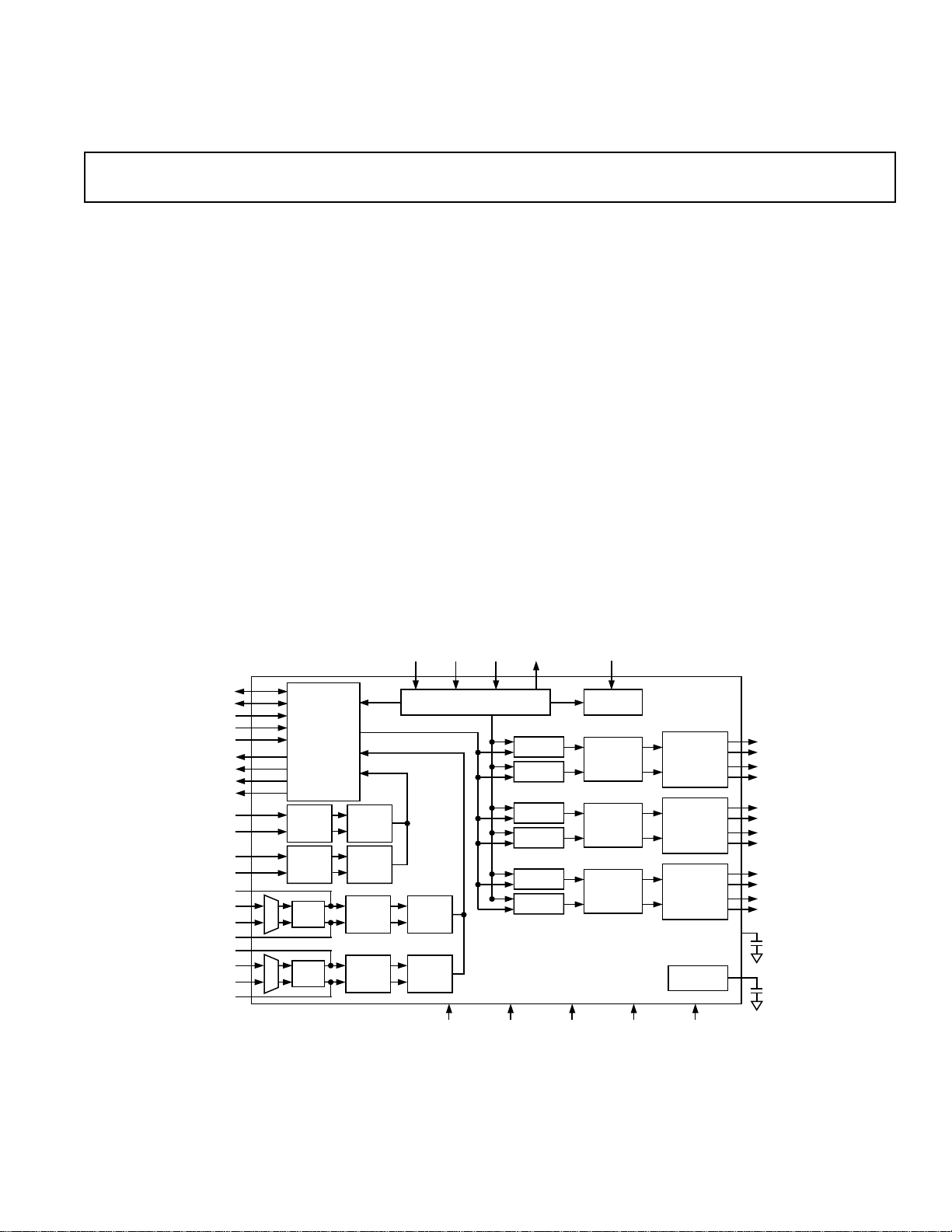
DLRCLK
DBCLK
DSDATA1
DSDATA2
DSDATA3
ALRCLK
ABCLK
ASDATA1
ASDATA2
AIN1L
AIN1R
CAPL1
AIN2L1
AIN2L2
CAPL2
CAPR1
AIN2R1
AIN2R2
CAPR2
MUX
MUX
SERIAL
DATA
PORT
ADC1L
48/96kHz
ADC1R
48/96kHz
PGA
PGA
I/O
FUNCTIONAL BLOCK DIAGRAM
DIGITAL
FILTER
48/96kHz
DIGITAL
FILTER
48/96kHz
ADC2L
48kHz
ADC2R
48kHz
CCLK CDATA CLATCH
CONTROL PORT
DIGITAL
FILTER
48kHz
DIGITAL
FILTER
48kHz
PWRDWN/RESET AVDD AGND DVDD DGND
COUT
VOLUME
VOLUME
VOLUME
VOLUME
VOLUME
VOLUME
2432
MCLK
CLOCK
DIGITAL
FILTER
DIGITAL
FILTER
DIGITAL
FILTER
DAC
DAC
DAC
V
REF
A
OUT
A
OUT
A
OUT
A
OUT
A
OUT
A
OUT
FILTD
FILTR
1
2
3
4
5
6
SHARC is a registered trademark of Analog Device, Inc.
REV.PrC
Information furnished by Analog Devices is believed to be accurate and
reliable. However, no responsibility is assumed by Analog Devices for its
use, nor for any infringements of patents or other rights of third parties
which may result from its use. No license is granted by implication or
otherwise under any patent or patent rights of Analog Devices.
One Technology Way, P.O. Box 9106, Norwood, MA 02062-9106, U.S.A.
Tel: 781/329-4700 World Wide Web Site: www.analog.com
Fax: 781/326-8703 © Analog Devices, Inc., 2001
Page 2

PRELIMINARY TECHNICAL DATA
AD1836–SPECIFICATIONS
TEST CONDITIONS UNLESS OTHERWISE NOTED
Supply Voltages (AVDD, DVDD) 5.0 V
Ambient Temperature 25°C
Master Clock 12.288 MHz, (48 kHz f
Input Signal 1.000 kHz, 0 dBFS (Full Scale)
Input Sample Rate 48 kHz
Measurement Bandwidth 20 Hz to 20 kHz
Word Width 20 Bits
Load Capacitance 100 pF
Load Impedance 47 kΩ
Input Voltage HI 2.4 V
Input Voltage LO 0.8 V
NOTE
Performance of all channels are identical (exclusive of the Interchannel Gain Mismatch and Interchannel Phase Deviation specifications).
ANALOG PERFORMANCE
ANALOG-TO-DIGITAL CONVERTERS
ADC Resolution (all ADCs) 24 Bits
Dynamic Range (20 Hz to 20 kHz, –60 dB Input)
No Filter 102 dB
With A-Weighted Filter 105 dB
Total Harmonic Distortion + Noise –92 dB
Interchannel Isolation 100 dB
Interchannel Gain Mismatch 0.01 dB
Programmable Input Gain 12 dB
Gain Step Size 3 dB
Offset Error LSB
Full-Scale Input Voltage At Each Pin (Single-Ended) 1.0 (2.8) V rms (V p-p)
Gain Drift 100 ppm/°C
Input Resistance 10 kΩ
Input Capacitance 15 pF
Common-Mode Input Volts 2.25 V
DIGITAL-TO-ANALOG CONVERTERS
Dynamic Range (20 Hz to 20 kHz, –60 dB Input)
No Filter 105 dB
With A-Weighted Filter 108 dB
Total Harmonic Distortion + Noise –95 dB
Interchannel Isolation 100 dB
Interchannel Gain Mismatch 0.01(0.12) dB (%)
DC Accuracy %
Gain Error ± 3.0 %
Interchannel Gain Mismatch 0.01 dB
Gain Drift 150 ppm/°C
Interchannel Crosstalk (EIAJ Method) –120 dB
Interchannel Phase Deviation ± 0.1 Degrees
Volume Control Step Size (1023 Linear Steps) 0.098 %
Volume Control Range (Max Attenuation) 60 dB
Mute Attenuation –100 dB
De-Emphasis Gain Error ± 0.1 dB
Full-Scale Output Voltage At Each Pin (Single-Ended) 1.0 (2.8) V rms (V p-p)
Output Resistance At Each Pin 115 Ω
Common-Mode Output 2.25 V
, 256 × fS Mode)
S
Min Typ Max Unit
–2–
REV. PrC
Page 3

PRELIMINARY TECHNICAL DATA
DIGITAL FILTERS at 44.1 kHz
Min Typ Max Unit
ADC DECIMATION FILTER
Pass Band 20 kHz
Pass Band Ripple ± 0.0001 dB
Transition Band 22 kHz
Stop Band 24 kHz
Stop Band Attenuation 120 dB
Group Delay TBD µs
DAC INTERPOLATION FILTER
Pass Band 20 kHz
Pass Band Ripple ± 0.01 dB
Transition Band 22 kHz
Stop Band 24 kHz
Stop Band Attenuation 70 dB
Group Delay TBD µs
TIMING
Parameter Min Max Unit Comments
MASTER CLOCK AND RESET
t
MH
t
ML
t
MCLK
f
MCLK
t
PDR
SPI PORT
t
CCH
t
CCL
t
CCP
t
CDS
t
CDH
t
CLS
t
CLH
t
CODE
t
COD
t
COH
t
COTS
DAC SERIAL PORT
Normal Modes
t
DBH
t
DBL
t
DBP
f
DB
t
DLS
t
DLH
t
DDS
t
DDH
Packed 128, 256 Modes
t
DBH
t
DBL
t
DBP
f
DB
t
DLS
t
DLH
t
DDS
t
DDH
MCLK High min max ns 256 × f
512 × f
768 × f
S
S
S
MCLK Low min max ns
MCLK Period min max ns
MCLK Freq min max ns
PD/RST Low 4500 MCLK Periods Reset to SPI Register Write
CCLK High min ns
CCLK Low min ns
CCLK Period min ns
CDATA Setup min ns To CCLK Rising
CDATA Hold min ns From CCLK Rising
CLATCH Setup min ns To CCLK Rising
CLATCH Hold min ns From CCLK Falling
COUT Enable max ns From CCLK Falling
COUT Delay max ns From CCLK Falling
COUT Hold min ns From CCLK Falling
COUT Three-State max ns From CCLK Falling
DBCLK High min ns
DBCLK Low min ns
DBCLK Period min ns
DBCLK Freq max ns
DLRCLK Setup min ns To DBCLK Rising
DLRCLK Hold min ns From DBCLK Rising
DSDATA Setup min ns To DBCLK Rising
DSDATA Hold min ns From DBCLK Rising
DBCLK High min ns
DBCLK Low min ns
DBCLK Period min ns
DBCLK Freq max ns
DLRCLK Setup min ns To DBCLK Rising
DLRCLK Hold min ns From DBCLK Rising
DSDATA Setup min ns To DBCLK Rising
DSDATA Hold min ns From DBCLK Rising
AD1836
REV. PrC–3–
Page 4

PRELIMINARY TECHNICAL DATA
AD1836–SPECIFICATIONS
TIMING (continued)
Parameter Min Max Unit Comments
ADC Serial Port
Normal Modes
t
ABH
t
ABL
t
ALS
t
ABDD
t
ALRDD
Packed 128, 256 Modes
t
ABH
t
ABL
t
ALS
t
ABDD
t
ALRDD
TDM PACKED AUX, MASTER MODE
t
ABH
t
ABL
t
XBH
t
XBL
t
ALS
t
XLS
t
ABDD
t
ALRDD
t
DDS
t
DDH
t
DDS
t
DDH
t
DXDD
t
DXDD
ABCLK Delay High max ns From MCLK Rising
256 × f
S
512 × f
S
768 × f
S
ABCLK Delay Low max ns From MCLK Rising
256 × f
S
512 × f
S
768 × f
S
LRCLK Delay max ns From ABCLK Falling
ASDATA Delay max ns From ABCLK Falling
ASDATA Delay max ns From ALRCLK Changing
(Left-Justified)
ABCLK Delay High max ns From MCLK Rising
256 × f
S
512 × f
S
768 × f
S
ABCLK Delay Low max ns From MCLK Rising
256× f
S
512 × f
S
768 × f
S
LRCLK Delay max ns From ABCLK Falling
ASDATA Delay max ns From ABCLK Falling
ASDATA Delay max ns From ALRCLK Changing
(Left-Justified)
ABCLK Delay High max ns From MCLK Rising
256 × f
S
512 × f
S
768 × f
S
ABCLK Delay Low max ns From MCLK Rising
256 × f
S
512 × f
S
768 × f
S
AUXBCLK Delay High max ns From MCLK Rising
256 × f
S
512 × f
S
768 × f
S
AUXBCLK Delay Low max ns From MCLK Rising
256 × f
S
512 × f
S
768 × f
S
LRCLK Delay max ns From ABCLK Falling
AUXLRCLK Delay max ns From ABCLK Falling
ASDATA Delay max ns From ABCLK Falling
ASDATA Delay max ns From ALRCLK Changing
(Left-Justified)
AAUXDATA Setup min ns To AUXBCLK Rising
AAUXDATA Hold min ns From AUXBCLK Rising
DSDATA Setup min ns To DBCLK Rising
DSDATA Hold min ns From DBCLK Rising
DAUXDATA Delay max ns From AUXBCLK Falling
DAUXDATA Delay max ns From AUXLRCLK Changing
(Left-Justified)
–4–
REV. PrC
Page 5

PRELIMINARY TECHNICAL DATA
TIMING (continued)
Parameter Min Max Unit Comments
TDM, PACKED AUX, SLAVE MODE
t
ABH
t
ABL
t
ABP
f
AB
t
ALS
t
ALH
t
ABDD
t
ALRDD
t
AXDS
t
AXDH
t
DDS
t
DDH
t
DXDD
t
DXDD
POWER SUPPLIES
Parameter Min Typ Max Unit
Supplies
Voltage, Analog and Digital 4.5 5 5.5 V
Analog Current 108 mA
Analog Current, Power-Down 47 mA
Digital Current 78 mA
Digital Current, Power-Down 1.5 mA
Dissipation
Operation, Both Supplies 930 mW
Operation, Analog Supply 540 mW
Operation, Digital Supply 390 mW
Power-Down, Both Supplies 243 mW
Power Supply Rejection Ratio
1 kHz 300 mV p-p Signal at Analog Supply Pins –60 dB
20 kHz 300 mV p-p Signal at Analog Supply Pins –50 dB
ABCLK High min ns
ABCLK Low min ns
ABCLK Period min ns
ABCLK Freq max ns
LRCLK Setup min ns To ABCLK Rising
LRCLK Hold min ns To ABCLK Rising
ASDATA Delay max ns From ABCLK Falling
ASDATA Delay max ns From ALRCLK Changing
(Left-Justified)
AAUXDATA Setup min ns To AUXBCLK Rising
AAUXDATA Hold min ns From AUXBCLK Rising
DSDATA Setup min ns To DBCLK Rising
DSDATA Hold min ns From DBCLK Rising
DAUXDATA Delay max ns From AUXBCLK Falling
DAUXDATA Delay max ns From AUXLRCLK Changing
(Left-Justified)
AD1836
TEMPERATURE RANGE
Parameter Min Typ Max Unit
Specifications Guaranteed 25 °C
Functionality Guaranteed –40 +85 °C
Storage –65 +150 °C
Specifications subject to change without notice.
REV. PrC–5–
Page 6
AD1836
WARNING!
ESD SENSITIVE DEVICE
PRELIMINARY TECHNICAL DATA
ABSOLUTE MAXIMUM RATINGS*
Parameter Min Max Unit
Power Supplies
Analog (AVDD) –0.3 6.0 V
Digital (DVDD) –0.3 6.0 V
Input Current ± 20 mA
(Except Supply Pins)
Analog Input Voltage –0.3 AVDD + 0.3 V
(Signal Pins)
Digital Input Voltage –0.3 DVDD + 0.3 V
(Signal Pins)
Ambient Temperature –40 +85 °C
(Operating)
ESD Tolerance 1 kV
(Human Body Model, Method 3015.2, MIL-STD-883B)
*Stresses greater than those listed under Absolute Maximum Ratings may cause
permanent damage to the device. This is a stress rating only; functional operation
of the device at these or any other conditions above those indicated in the
operational section of this specification is not implied. Exposure to absolute
maximum rating conditions for extended periods may affect device reliability.
ORDERING INFORMATION
Model Temperature Package Package
Range Description Option
AD1836AS –40 to +85°C 52-Lead MQFP S-52
DVDD
CDATA
PD/RST
OUTLP3
OUTLN3
OUTLP2
OUTLN2
OUTLP1
OUTLN1
AVDD
AGND
FILTD
FILTR
PIN CONFIGURATION
52-Lead MQFP
DGND
CCLK
CLATCH
COUT
ASDATA2
ASDATA1
ODVDD
MCLK
CAPL2
CAPL1
ADC1INRN
ALRCLK
ADC2INL1
52 51 50 49 48 43 42 41 4047 46 45 44
1
PIN 1
2
IDENTIFIER
3
4
5
6
7
8
9
10
11
12
13
14 15 16 17 18 19 20 21 22 23 24 25 26
AVDD
AGND
AD1836
TOP VIEW
(Not to Scale)
ADC1INLP
ADC1INLN
ADC1INRP
ABCLK
DSDATA3
DSDATA2
ADC2INL2
ADC2INR2
ADC2INR1
DVDD
39
38
37
36
35
34
33
32
31
30
29
28
27
CAPR1
DGND
DSDATA1
DBCLK
DLRCLK
OUTRP3
OUTRN3
OUTRP2
OUTRN2
OUTRP1
OUTRN1
AGND
AGND
CAPR2
CAUTION
ESD (electrostatic discharge) sensitive device. Electrostatic charges as high as 4000 V readily
accumulate on the human body and test equipment and can discharge without detection. Although
the AD1836 features proprietary ESD protection circuitry, permanent damage may occur on
devices subjected to high-energy electrostatic discharges. Therefore, proper ESD precautions are
recommended to avoid performance degradation or loss of functionality.
–6–
REV. PrC
Page 7

PRELIMINARY TECHNICAL DATA
AD1836
PIN FUNCTION DESCRIPTIONS
PIN
No. Mnemonic In/Out Description
1, 40 DVDD I Digital Power Supply. Connect to digital 5 V supply.
2 CDATA I Serial Control Input
3 PD/RST I Power-Down Reset
4 OUTLP3 O DAC 3 (Left) Positive Output
5 OUTLN3 O DAC 3 (Left) Negative Output
6 OUTLP2 O DAC 2 (Left) Positive Output
7 OUTLN2 O DAC 2 (Left) Negative Output
8 OUTLP1 O DAC 1 (Left) Positive Output
9 OUTLN1 O DAC 1 (Left) Negative Output
10, 15 AVDD I Analog Power Supply. Connect to analog 5 V.
11, 14, 28, 29 AGND I Analog Ground
12 FILTD I Filter Capacitor Connection. Recommend 10 µF//100 nF.
13 FILTR I Voltage Reference Filter Capacitor Connection. Recommend 10 µF//100 nF.
16 ADC1INLP I ADC1 Left Positive Input
17 ADC1INLN I ADC1 Left Negative Input
18 ADC1INRP I ADC1 Right Positive Input
19 ADC1INRN I ADC1 Right Negative Input
20 ADC2INL+/CAPL2 I ADC2 Left Positive Input (Direct Mode)/ADC2 Left Decoupling Cap
(MUX/PGA and PGA Differential Mode)
21 ADC2INL–/CAPL1 I ADC2 Left Negative Input (Direct Mode)/ADC2 Left Decoupling Cap
(MUX/PGA and PGA Differential Mode)
22 ADC2INL1 I ADC2 Left Input 2 (MUX/PGA Mode)/Left Positive Input (PGA Differ-
ential Mode)
23 ADC2INL2 I ADC2 Left Input 1 (MUX/PGA Mode)/Left Negative Input (PGA Differ-
ential Mode)
24 ADC2INR2 I ADC2 Right Input 1 (MUX/PGA Mode)/Right Negative Input (PGA
Differential Mode)
25 ADC2INR1 I ADC2 Right Input 2 (MUX/PGA Mode)/Right Positive Input (PGA
Differential Mode)
26 ADC2INR–/CAPR1 I ADC2 Right Negative Input (Direct Mode)/ADC2 Right Decoupling Cap
(MUX/PGA and PGA Differential Mode)
27 ADC2INR+/CAPR2 I ADC2 Right Positive Input (Direct Mode)/ADC2 Right Decoupling Cap
(MUX/PGA and PGA Differential Mode)
30 OUTRN1 O DAC 1 (Right) Negative Output
31 OUTRP1 O DAC 1 (Right) Positive Output
32 OUTRN2 O DAC 2 (Right) Negative Output
33 OUTRP2 O DAC 2 (Right) Positive Output
34 OUTRN3 O DAC 3 (Right) Negative Output
35 OUTRP3 O DAC 3 (Right) Positive Output
36 DLRCLK I/O LR Clock for DACs
37 DBCLK I/O Bit Clock for DACs
38 DSDATA1 I DAC Input #1 (Input to DAC1 and DAC2)
39, 52 DGND I Digital Ground
41 DSDATA2 I DAC Input #2 (Input to DAC3 and DAC4)
42 DSDATA3 I DAC Input #3 (Input to DAC5 and DAC6)
43 ABCLK O Bit Clock for ADCs
44 ALRCLK O LR Clock for ADCs
45 MCLK I Master Clock Input
46 ODVDD I Digital Output Driver Power Supply
47 ASDATA1 O ADC Serial Data Output #1
48 ASDATA2 O ADC Serial Data Output #2
49 COUT O Output for Control Data
50 CLATCH I Latch Input for Control Data
51 CCLK I Control Clock Input for Control Data
52 DGND I Digital Ground
REV. PrC
–7–
Page 8

AD1836
PRELIMINARY TECHNICAL DATA
AVDD DVDD ODVDD
2 2 1
AIN1L
AIN1R
CAPL
AIN2L
A
IN
CAPR
OUTL1
OUTR1
OUTL2
OUTR2
OUTL3
OUTR3
FILTR
ADCI L/R
48/96kHz
PGA
L/R
2R
MUX
DAC 1
L/R
DAC 2
L/R
DAC 3
L/R
V
REF
AGND FILTD DGND
4
ADC2L/R
48/96kHz
(MAX)
INTERPOLATION
FILTER
INTERPOLATION
FILTER
INTERPOLATION
FILTER
AD1836
DECIMATION
FILTER
48/96kHz
DECIMATION
FILTER
48kHz (MAX)
VOLUME
CONTROL
VOLUME
CONTROL
VOLUME
CONTROL
2
ADC
SERIAL
INTERFACE
DAC
SERIAL
INTERFACE
SPI
CONTROL
PORT
SDOUT1
SDOUT2
ABCLK
ALRCLK
MCLK
DLRCLK
DBCLK
SDIN1
SDIN2
SDIN3
RESET
CCLK
CLATCH
CDATA
COUT
Figure 1.
FUNCTIONAL OVERVIEW
ADCs
There are four ADC channels in the AD1836, configured as two
independent stereo pairs. One stereo pair is the primary ADC and
has fully differential inputs. The second pair can be programmed
to operate in one of three possible input modes (programmed
via SPI ADC Control Register 3). The ADC section may also
operate at a sample rate of 96 kHz, with only the two primary
channels active. The ADCs include an on-board digital decimation filter with 120 dB stopband attenuation and linear phase
response, operating at an oversampling ratio of 128 (for 4-channel
48 kHz operation) or 64 (for two-channel 96 kHz operation).
The primary ADC pair should be driven from a differential
signal source for best performance. The input pins of the primary ADC connect directly to internal switched capacitors. To
isolate the external driving op amp from the “glitches” caused
by the internal switched-capacitors, each input pin should be
isolated by using a series-connected external 100 Ω resistor
together with a 1 nF capacitor connected from each input to
ground. This capacitor must be of high quality; for example,
ceramic NPO or polypropylene film.
The secondary input pair can be operated in one of the following three modes:
1. Direct differential inputs (driven the same as the primary
ADC inputs described above).
2. PGA mode with differential inputs (Figure 13). In this mode,
the PGA amplifier can be programmed using the SPI port to
give an input gain of 0 to 12 dB in 3 dB steps. External
capacitors are used after the PGA to supply filtering for the
switched-capacitor inputs.
3. Single-ended MUX/PGA mode. In this mode, two singleended stereo inputs are provided that can be selected using
the SPI port. Input gain can be programmed from 0 dB to
12 dB in steps of 3 dB External capacitors are used to supply
filtering for the switched-capacitor inputs.
–8–
ADC peak level information for each ADC may be read from
the SPI port through Registers 12 through 15. The data is supplied as a 10-bit word with a maximum range of 0 dB to –60 dB
and a resolution of 1 dB. The registers will hold peak information until read; after reading, the registers are reset so that new
peak information can be acquired. Refer to the register description for details of the format.
The voltage at the V
pin, FILTR (~2.25 V) can be used to
REF
bias external op amps used to buffer the input signals. This
source can be connected directly to op amp inputs but should
be buffered if it is required to drive resistive networks.
DACs
The AD1836 has six DAC channels arranged as three independent stereo pairs, with six fully differential analog outputs for
improved noise and distortion performance. Each channel has
its own independently programmable attenuator, adjustable in
1024 linear steps. Digital inputs are supplied through three
serial data input pins (one for each stereo pair) and a common
frame (DLRCLK) and bit (DBLCK) clock. Alternatively, one
of the “packed data” modes may be used to access all six channels on a single TDM data pin.
Each set of differential output pins sits at a dc level of V
REF
, and
swings ± 1.4 V for a 0 dB digital input signal. A single op amp
third-order external low-pass filter is recommended to remove
high-frequency noise present on the output pins, as well as to
provide differential-to-single-ended conversion. A recommended
circuit is shown in Figure 2. Note that the use of op amps with
low slew rate or low bandwidth may cause high-frequency noise
and tones to fold down into the audio band; care should be
exercised in selecting these components.
The FILTD pin should be connected to an external grounded
capacitor. This pin is used to reduce the noise of the internal
DAC bias circuitry, thereby reducing the DAC output noise. In
some cases this capacitor may be eliminated with little effect on
performance. The voltage at the V
pin, FILTR (~2.25 V) can
REF
be used to bias external op amps used to buffer the output signals.
REV. PrC
Page 9

CLATCH
CCLK
PRELIMINARY TECHNICAL DATA
AD1836
CDATA
COUT
D15
D9
D8 D0
Figure 2. Format of SPI Signal
Clock Signals
The master clock frequency can be selected for 256, 512, or
768 times the sample rate. The default at power-up is 256 f
.
S
For operation at 96 kHz, the master clock frequency should
stay at the same absolute frequency. For example, if the AD1836
is programmed in 256 × f
mode and operated in the normal
S
48 kHz 4-channel mode, the frequency of the master-clock
would be 256 × 48 kHz = 12.288 MHz. If the AD1836 is then
switched to 96 kHz operation (via writing to the SPI port), the
frequency of the master-clock should remain at 12.288 MHz
(which is now 128 × f
The internal clock used in the AD1836 is 512 × f
mode) or 512 × f
).
S
(48 kHz
(96 kHz mode). Clock doublers are used to
S
S
generate this internal master-clock from the external clocks.
Since clock-doublers have a limited range of operation, it is
recommended that the part be operated in 512 × f
mode if the
S
desired sampling rates are not at all close to the common audio
sampling rates for which the part was designed.
To maintain the highest performance possible, it is recommended
that the clock jitter of the master clock signal be limited to less
than 300 ps rms, measured using the edge-to-edge technique.
Even at these levels, extra noise or tones may appear in the
DAC outputs if the jitter spectrum contains large spectral peaks.
It is highly recommended that the master clock be generated by
an independent crystal oscillator. In addition, it is especially
important that the clock signal should not be passed through an
FPGA or other large digital chip before being applied to the
AD1836. In most cases this will induce clock jitter due to the
fact that the clock signal is sharing common power and ground
connections with other unrelated digital output signals.
The six DAC channels use a common serial bit clock to clock in
the serial data and a common left-right framing clock. The four
ADC channels output a common serial bit clock and a left-right
framing clock. The clock signals are all synchronous with the
sample rate.
RESET and Power-Down
RESET will power down the chip and set the control registers
to their default settings. After reset is deasserted, an initialization
routine will run inside the AD1836 to clear all memories to zero.
This initialization lasts for approximately 20 LRCLK intervals.
During this time it is recommended that no SPI writes occur.
Serial Control Port
The AD1836 has an SPI-compatible control port to permit
programming the internal control registers for the ADCs and
D0D14
DACs and for reading the ADC signal level from the internal
peak detectors. The DAC output levels may be independently
programmed by means of an internal digital attenuator adjustable in 1024 linear steps.
The SPI control port is a 4-wire serial control port. The format is
similar to the Motorola SPI format except the input data word
is 16-bits wide. Max serial bit clock frequency is 8 MHz and
may be completely asynchronous to the sample rate of the ADCs
and DACs. The following figure shows the format of the SPI
signal. Note that the CCLK should be run continuously and not
stop between SPI transactions.
Power Supply and Voltage Reference
The AD1836 is designed for 5 V supplies. Separate power supply pins are provided for the analog and digital sections. These
pins should be bypassed with 100 nF ceramic chip capacitors, as
close to the pins as possible, to minimize noise pickup. A bulk
aluminum electrolytic capacitor of at least 22 µF should also be
provided on the same PC board as the codec. For critical applications, improved performance will be obtained with separate
supplies for the analog and digital sections. If this is not possible, it is recommended that the analog and digital supplies be
isolated by means of two ferrite beads in series with the bypass
capacitor of each supply. It is important that the analog supply
be as clean as possible.
The internal voltage reference is brought out on Pin 13 (FILTR)
and should be bypassed as close as possible to the chip, with a
parallel combination of 10 µF and 100 nF. The reference volt-
age may be used to bias external op amps to the common-mode
voltage of the analog input and output signal pins. The current
drawn from the V
Serial Data Ports—Data Format
pin should be limited to less than 50 µA.
REF
The ADC serial data output mode defaults to the popular I2S
format, where the data is delayed by 1 BCLK interval from the
edge of the LRCLK. By changing Bits 8 and 9 in ADC Control
Register 2, the serial mode can be changed to Right-Justified
(RJ), Left-Justified DSP (DSP) or Left-Justified (LJ). In the RJ
mode, it is necessary to set Bits 6 and 7 to define the width of
the data word.
The DAC serial data input mode defaults to I
2
S. By changing
Bits 5, 6, and 7 in DAC Control Register 1, the mode can be
changed to RJ, DSP, LJ, Packed Mode 1 or Packed Mode 2.
REV. PrC
–9–
Page 10

AD1836
PRELIMINARY TECHNICAL DATA
The word width defaults to 24 bits but can be changed by
reprogramming Bits 3 and 4 in DAC Control Register 1. The
packed modes accept six channels of data at the DSDATA1
input pin which is independently routed to each of the six
internal DACs.
A special “auxiliary mode” is provided to allow two external
stereo ADCs and one external stereo DAC to be interfaced to
the AD1836 to provide 8-in/8-out operation. In addition, this
mode supports glueless interface to a single SHARC DSP serial
port, allowing a SHARC DSP to access all eight channels of
analog I/O. In this special mode, many pins are redefined; see
Table I for a list of redefined pins. Two versions of this mode
are available. In the “master” mode, the AD1836 provides the
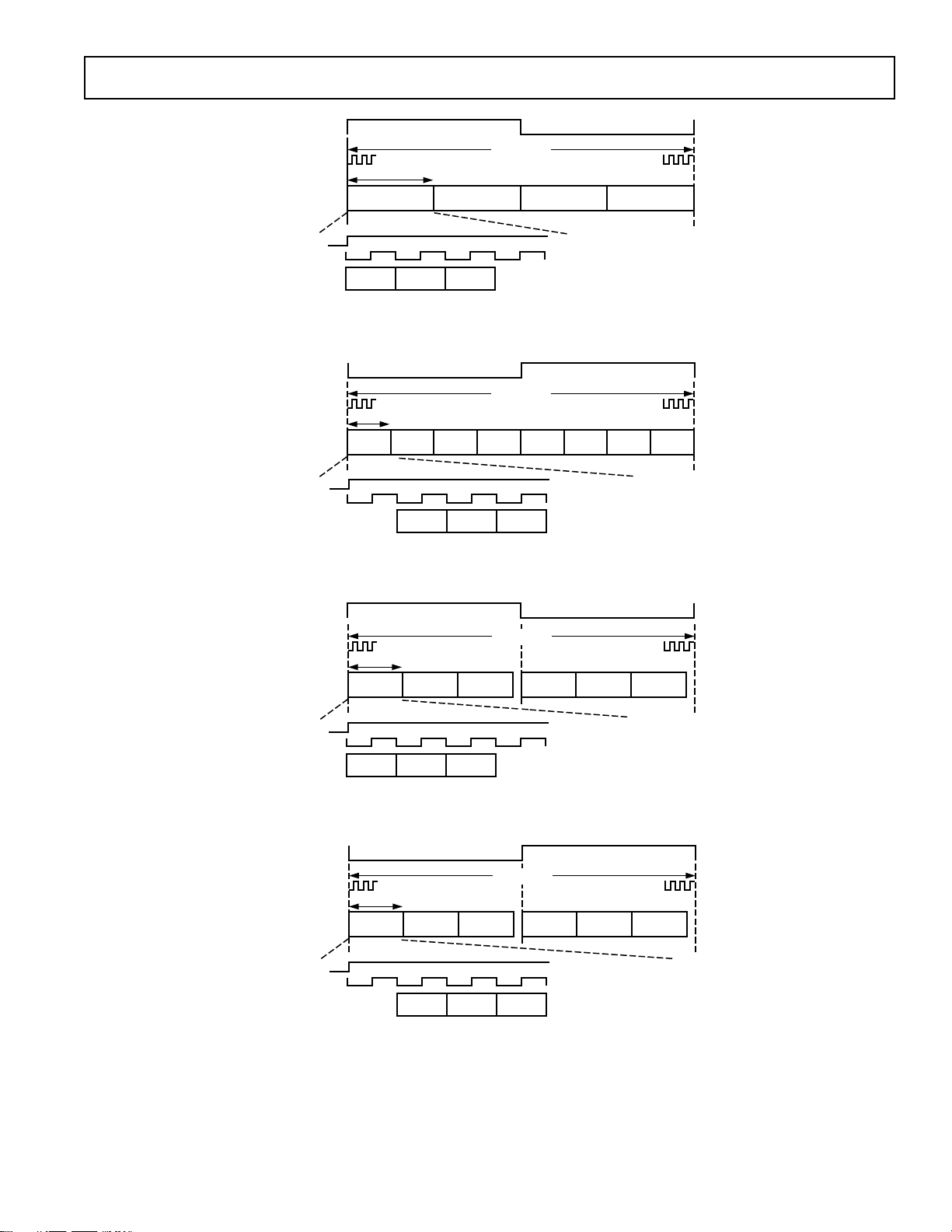
LRCLK
BCLK
SDATA
LRCLK
MSB
LEFT CHANNEL RIGHT CHANNEL
LSB
LEFT-JUSTIFIED MODE – 16 TO 24 BITS PER CHANNEL
LEFT CHANNEL
LRCLK and BCLK signals, and the external ADCs operate in
slave mode. In the “slave” mode, the external ADCs provide the
LRCLK and BCLK signals (which must be divided down properly from the external master clock), and the AD1836 will sync
to these external clocks. See Figures 8 through 10 for details of
this mode. Figure 11 shows the internal signal-flow diagram of
the auxiliary mode.
The following figures show the serial mode formats.
MSB
RIGHT CHANNEL
LSB
BCLK
SDATA
LRCLK
BCLK
SDATA
LRCLK
BCLK
SDATA
MSB MSB
LEFT CHANNEL RIGHT CHANNEL
MSB MSB
RIGHT-JUSTIFIED MODE – SELECT NUMBER OF BITS PER CHANNEL
MSB MSB
NOTES
1. DSP MODE DOES NOT IDENTIFY CHANNEL
2. LRCLK NORMALLY OPERATES AT f
3. BCLK FREQUENCY IS NORMALLY 64 LRCLK BUT MAY BE OPERATED IN BURST MODE
EXCEPT FOR DSP MODE WHICH IS 2 f
S
LSB LSB
12S MODE – 16 TO 24 BITS PER CHANNEL
LSB LSB
LSB LSB
DSP MODE – 16 TO 24 BITS PER CHANNEL
1/f
S
S
Figure 3. Stereo Serial Modes
–10–
REV. PrC
Page 11
PRELIMINARY TECHNICAL DATA
LRCLK
SLOT 2
LEFT 1
128 BCLKs
256 BCLKs
SLOT 5
RIGHT 0
SLOT 3
RIGHT 0
RIGHT 1
SLOT 6
SLOT 4
RIGHT 1
BCLK
DATA
LRCLK
BCLK
DATA
32 BCLKs
SLOT 1
LEFT 0
MSB MSB–1MSB–2
Figure 4. ADC Packed Mode 128
32 BCLKs
SLOT 1
SLOT 2
LEFT 0
SLOT 3 SLOT 4 SLOT 7 SLOT 8
LEFT 1
AD1836
LRCLK
BCLK
DATA
LRCLK
BCLK
DATA
MSB MSB–1MSB–2
Figure 5. ADC Packed Mode 256
128 BCLKs
20 BCLKs
SLOT 1
LEFT 0
MSB MSB–1 MSB–2
SLOT 2
LEFT 1
SLOT 3
LEFT 2
RIGHT 0
Figure 6. DAC Packed Mode 128
256 BCLKs
32 BCLKs
SLOT 1
LEFT 0
SLOT 2
LEFT 1
MSB MSB–1MSB–2
SLOT 3
LEFT 2
RIGHT 0
SLOT 4
SLOT 4
LRCLK
BCLK
DATA
LRCLK
BCLK
DATA
SLOT 5
RIGHT 1
SLOT 5
RIGHT 1
SLOT 6
RIGHT 2
SLOT 6
RIGHT 2
REV. PrC
Figure 7. DAC Packed Mode 256
–11–
Page 12

AD1836
FSTDM
BCLK
TDM
ASDATA1
TDM (OUT)
PRELIMINARY TECHNICAL DATA
MSB TDM
1ST
CH
MSB TDM
8TH
CH
ASDATA1
TDM INTERFACEAUX – I
S INTERFACE
2
DSDATA1
TDM (IN)
DSDATA1
LRCLK I
(FROM AUX ADC#1)
(FROM AUX ADC#1)
(FROM AUX ADC#1)
(FROM AUX ADC#2)
BCLK I
AAUXDATA1 (IN)
AAUXDATA2 (IN)
DAUXDATA (OUT)
(TO AUX DAC)
INTERNAL
ADC L0
32
MSB TDM
1ST
CH
INTERNAL
DAC L0
32
AUX
2
S
AUX
2
S
NOTE:
AUX BCLK FREQUENCY IS 64 FRAME-RATE; TDM BCLK FREQUENCY IS 256 FRAME-RATE.
INTERNAL
ADC L1
INTERNAL
DAC L1
AUX_ADC L0
INTERNAL
DAC L2
LEFT
AUX_ADC L1
AUX_DAC L0
INTERNAL
ADC R0
INTERNAL
DAC R0
Figure 8. AUX-Mode Timing
INTERNAL
ADC R1
INTERNAL
DAC R1
AUX_ADC R0
INTERNAL
DAC R2
RIGHT
2
S – MSB RIGHTI2S – MSB LEFT
I
I2S – MSB RIGHTI2S – MSB LEFT
2
I
S – MSB RIGHTI2S – MSB LEFT
AUX_ADC R1
MSB TDM
8TH
CH
AUX_DAC R0
–12–
REV. PrC
Page 13

PRELIMINARY TECHNICAL DATA
AD1836
ADC #1
SLAVE
ADC #2
SLAVE
LRCLK
BCLK
DATA
MCLK
LRCLK
BCLK
DATA
MCLK
SHARC IS ALWAYS
RUNNING IN SLAVE MODE
(INTERRUPT-DRIVEN)
TxDATA
)
S
30MHz
12.288MHz
SHARC
FSYNC-TDM (RFS)
RxDATA
RxCLK
ASDATA1 ALRCLK ABCLK DSDATA1
DLRCLK/AUXLRCLK
DSDATA2/AAUXDATA1
DSDATA3/AAUXDATA2
MCLK
TFS (NC)
DBCLK/AUXBCLK (64f
ASDATA2/DAUXDATA
TxCLK
AD1836+
MASTER
Figure 9. AUX–Mode Connection to SHARC (Master Mode)
SHARC
30MHz
SHARC IS ALWAYS
RUNNING IN SLAVE MODE
(INTERRUPT-DRIVEN)
LRCLK
BCLK
DATA
MCLK
DAC
ADC #1
MASTER
ADC #2
SLAVE
LRCLK
BCLK
DATA
MCLK
LRCLK
BCLK
DATA
MCLK
12.288MHz
RxDATA
RxCLK
ASDATA1 ALRCLK ABCLK DSDATA1
DLRCLK/AUXLRCLK
DSDATA2/AAUXDATA1
DSDATA3/AAUXDATA2
MCLK
TFS (NC)
TxCLK
DBCLK/AUXBCLK (64f
ASDATA2/DAUXDATA
AD1836+
SLAVE
TxDATA
)
S
FSYNC-TDM (RFS)
Figure 10. AUX–Mode Connection to SHARC (Slave Mode)
LRCLK
BCLK
DATA
MCLK
DAC
REV. PrC
–13–
Page 14

PRELIMINARY TECHNICAL DATA
AD1836
Table I. Pin Function Changes in AUX-Mode
Pin Name (I2S/AUX-Mode) I2S-Mode AUX-Mode
2
ASDATA1(O) I
ASDATA2(O)/DAUXDATA(O) I
DSDATA1(I) I
DSDATA2(I)/AAUXDATA(I) I
DSDATA3(I)/AAUXDATA2(I) I
ALRCLK(O) LRCLK for Internal ADC1, 2 TDM Frame Sync Out, to SHARC
ABCLK(O) BCLK for Internal ADC1, 2 TDM BCLK Out, to SHARC
DLRCLK(I)/AUXLRCLK(I/O) LRCLK In/Out Internal DACs AUX LRCLK IN/OUT, Driven by Ext. IRCLK
DBCLK(I)/AUXBCLK(I/O) BCLK In/Out Internal DACs AUX BCLK IN/OUT, Drive by Ext. BCLK
S Data Out, Internal ADC1 TDM Data Out, to SHARC
2
S Data Out, Internal ADC2 AUX–I2S-Data Out (to Ext. DAC)
2
S Data In, Internal DAC1 TDM Data In, from SHARC
2
S Data In, Internal DAC2 AUX–I2S-Data in 1 (from Ext. ADC)
2
S Data in Internal DAC3 AUX–I2S-Data in 2 (from Ext. ADC)
from ADC (in Slave Mode). In Master Mode,
Driven by Internal MCLK/512.
from ADC (in Slave Mode). In Master Mode,
Driven by Internal MCLK/8.
FROM SHARC
FROM EXT A/D
FROM EXT A/D
DLRCLK/AUXLRCLK
DBCLK/AUXBCLK
DSDATA2/AUXDATA1
DSDATA3/AUXDATA2
DSDATA1
MASTER/SLAVE MODE,
FROM ADC SPI PORT
MCLK
2
S
1
TIMING GEN
LRCLK BCLK
AUXBCLK
AUXLRCLK
AUXDATA2
AUXDATA1
DSDATA1
DSDATA2
DSDATA3
LRCLK
BCLK
ADC
2
1
S
DECODE
MUX
MUX
INDICATES MUX POSITION FOR AUX-TDM MODE
SYNC SIGNAL DERIVED FROM AUXLRCLK USED TO
RESET INTERNAL ADC COUNTER
SYNC
4 ADC
SPORT
S
ASDATA1
AUXDATA
AUXLRCLK
SPORT
DAC
ASDATA1
2
1
S FORMATTER
AUXBCLK
CHANNELS
LRCLK
ABCLK
6 MAIN
MUX
2 AUX
CHANNELS
ALRCLK
ABCLK
ASDATA1
DATA TO SHARC
6-CH
DAC
ASDATA2/DAUXDATA
DATA TO EXT DAC
BCLK AND LRCLK FOR
EXT DAC COMES FROM
ADC BCLK, LRCLK.
MUST BE IN 1
2
S MODE
Figure 11. Extended TDM Mode Internal Flow Diagram
–14–
REV. PrC
Page 15

PRELIMINARY TECHNICAL DATA
AD1836
SPI CONTROL REGISTERS
Note: All control registers default to zero at power-up.
Serial SPI Word Format
Register Address Read/Write Reserved Data Field
15..12 11 10 9..0
4 Bits 1 = Read 0 10 Bits
0 = Write
Register Addresses and Functions
Register Address RD/WR RSVD Function
Bit 15 Bit 14 Bit 13 Bit 12 Bit 11 Bit 10 (Bits 9:0)
0 0 0 0 0 0 DAC Control 1
0 0 0 1 0 0 DAC Control 2
0 0 1 0 0 0 DAC Volume 0
0 0 1 1 0 0 DAC Volume 1
0 1 0 0 0 0 DAC Volume 2
0 1 0 1 0 0 DAC Volume 3
0 1 1 0 0 0 DAC Volume 4
0 1 1 1 0 0 DAC Volume 5
1 0 0 0 0 0 ADC 0 – Peak Level (Read Only)
1 0 0 1 0 0 ADC 1 – Peak Level (Read Only)
1 0 1 0 0 0 ADC 2 – Peak Level (Read Only)
1 0 1 1 0 0 ADC 3 – Peak Level (Read Only)
1 1 0 0 0 0 ADC Control 1
1 1 0 1 0 0 ADC Control 2
1 1 1 0 0 0 ADC Control 3
1 1 1 1 0 0 Reserved
DAC Control Register 1
Function
Data Word Power-Down Interpolator
Address RD/WR RSVD De-Emphasis Serial Mode Width Reset Mode Reserved
15, 14, 13, 12 11 10 9, 8 7, 6, 5 4, 3 2 1 0
2
0000 0 0 00 = None 000 = I
01 = 44.1 kHz 001 = RJ 01 = 20 Bits 1 = PWRDWN 1 = 4 × (96 kHz)
10 = 32.0 kHz 010 = DSP 10 = 16 Bits
11 = 48.0 kHz 011 = LJ 11 = Reserved
100 = Pack Mode 256
101 = Pack Mode 128
110 = Reserved
111 = Reserved
NOTES
Packed Mode: Four channels are “packed” into DSDATA1 serial input.
Packed Mode 128: Refer Figure 6.
Packed Mode 256: Refer to Figure 7.
S 00 = 24-Bits 0 = Normal 0 = 8 × (48 kHz) 0
REV. PrC
–15–
Page 16

PRELIMINARY TECHNICAL DATA
AD1836
DAC Control Register 2
Address RD/WR Reserved Mute DAC
15, 14, 13, 12 11 10, 9, 8, 7, 6 543210
0001 0 00000 0 = On 0 = On 0 = On 0 = On 0 = On 0 = On
1 = Mute5 1 = Mute4 1 = Mute3 1 = Mute2 1 = Mute1 1 = Mute0
DAC Volume Registers
Address RD/WR Reserved Volume
15, 14, 13, 12 11 10 9:0
0010: DAC 0 0 0 0 to 1023 in 1024 Linear Steps
0011: DAC 1
0100: DAC 2
0101: DAC 3
0110: DAC 4
0111: DAC 5
ADC Control Register 1
Address RD/WR RSVD Filter Power-Down Sample Rate Left Gain Right Gain
15, 14, 13, 12 11 9, 10 8 7 6 5, 4, 3 2, 1, 0
1100 0 00 0 = DC 0 = Normal 0 = 48 kHz 000 = 0 dB 000 = 0 dB
1 = High-Pass 1 = PWRDWN 1 = 96 kHz 001 = 3 dB 001 = 3 dB
NOTE
High-Pass Filter: 3 Hz High-Pass Filter.
Function
Function
Function
010 = 6 dB 010 = 6 dB
011 = 9 dB 011 = 9 dB
100 = 12 dB 100 = 12 dB
101 = Rsrvd 101 = Rsrvd
110 = Rsrvd 110 = Rsrvd
111 = Rsrvd 111 = Rsrvd
ADC Control Register 2
Master/Slave SOUT Word
ADC Mute
Address RD/WR RSVD AUX Mode Mode Width Right Left Right Left
15, 14, 13, 12 11 10 9 8, 7, 6 5, 4 3 2 1 0
2
1101 0 0 0 = Slave 000 = I
S 00 = 24 Bits 0 = On 0 = On W/Gain W/Gain
1 = Master 001 = RJ 01 = 20 Bits 1 = Mute3 1 = Mute2 0 = On 0 = On
010 = DSP 10 = 16 Bits 1 = Mute1 1 = Mute0
011 = LJ 11 = Invalid
100 Packed 256
101 Packed 128
110 Packed
AUX*
NOTES
*Note that Packed AUX mode affects the entire chip, including the DAC serial mode.
Packed Mode: Four channels are packed into ASDATA1 serial output.
Packed Mode 128: Refer Figure 4.
Packed Mode 256: Refer to Figure 5.
Packed AUX: Refer to Figures 8 to 11.
–16–
REV. PrC
Page 17

PRELIMINARY TECHNICAL DATA
AD1836
ADC Control Register 3
Function
Left Left Right Right
Clock Left Diff. Right Diff. MUX/PGA MUX MUX/PGA MUX
Address RD/WR Reserved Mode I/P Select I/P Select Enable I/P Select Enable I/P Select
15, 14, 13, 12 11 10, 9, 8 7, 6 5 4 3 2 1 0
1110 0 000 00 = 256 × f
01 = 512 × f
10 = 768 × f
*
When changing clock doubler bypass mode, other SPI bits that are written during the same SPI transaction may be lost. It is therefore recommended that a separate
transaction be used for setting CLKDBL Bypass Mode.
ADC Peak Level Data Registers
Address RD/WR RSVD 6-Data Bits 4-Fixed Bits
15, 14, 13, 12 11 10 9..4 3..0
1000 = ADC0 1 0 000000 = 0.0 dBFS 0000
1001 = ADC1 000001 = –1.0 dBFS
1010 = ADC2 000010 = –2.0 dBFS
1011 = ADC3 000011 = –3.0 dBFS The four LSBs are always zero.
0 = Differential 0 = Differential 0 = Direct 0 = I/P 0 0 = Direct 0 = I/P 0
S
PGA Mode. PGA Mode. 1 = MUX/ 1 = I/P 1 1 = MUX/ 1 = I/P 1
S
1 = PGA/MUX 1 = PGA/MUX PGA PGA
S
Mode (Single- Mode (SingleEnded Input) Ended Input)
Peak Level Data (10 Bits)
.
.
.
111111 = –63 dBFS
AD1836
CAP1L
C1
1nF
–
LEFT
INPUT #1
LEFT
INPUT #2
C2
1nF
NOTE
ADC2 SINGLE-ENDED MUX PGA INPUT MODE – LEFT CHANNEL ONLY SHOWN
CONTROL REGISTER 3 CONTENTS: 6 LSBS: SELECT INPUT #1: 11 1010
MUX
CAP2L
+
V
REF
–
+
V
REF
250
250
PGA
SELECT INPUT #2: 11 1111
GAIN SELECT
POWER-DOWN
ADC2L
INPUT SELECT
Figure 12. Single-Ended MUX/PGA Mode
AD1836
CAP1L
C1
1nF
LEFT + VE
INPUT
V
LEFT – VE
INPUT
CAP2L
C2
1nF
NOTE
ADC2 DIFFERENTIAL PGA INPUT MODE – LEFT CHANNEL ONLY SHOWN
CONTROL REGISTER 3 CONTENTS: 6 LSBS: 00 1010
REF
–
+
+
–
250
250
Figure 13. Differential Mode
ADC2L
GAIN SELECT
POWER-DOWN
REV. PrC
–17–
Page 18

AD1836
PRELIMINARY TECHNICAL DATA
52-Lead MQFP
(S-52)
0.037 (0.95)
0.031 (0.80)
0.026 (0.65)
0.010 (0.25)
MIN
40
PIN 1
1
0.026 (0.65)
BSC
SEATING
PLANE
0.557 (14.15)
0.547 (13.90) SQ
0.537 (13.65)
TOP VIEW
(PINS DOWN)
0.015 (0.38)
0.009 (0.22)
2739
1452
13
0.096 (2.45)
MAX
0.307
(7.80)
REF
0.083 (2.10)
0.079 (2.00)
0.077 (1.95)
0.009 (0.23)
0.005 (0.13)
DIMENSIONS PER JEDEC STANDARDS MO-112
CONTROLLING DIMENSIONS ARE IN MILLIMETERS
26
0.398 (10.11)
0.394 (10.00) SQ
0.390 (9.91)
7
0
–18–
REV. PrC
 Loading...