

Page 1

a
SoundPort® Controller
AD1816A
FEATURES
Compatible with Microsoft
®
PC 97 Logo Requirements
Supports Applications Written for Windows
Windows 3.1, Windows NT, SoundBlaster
AdLib
®
/OPL3
®
Stereo Audio 16-Bit SD Codec
Internal 3D Circuit—Phat™
Stereo Phase Expander
MPC Level-3 Mixer
ISA Plug and Play Compatible
16-Bit Address Decode
Dual Type F FIFO DMA Support
MPU-401 Compatible MIDI Port
Supports Wavetable Synthesizers
Integrated Enhanced Digital Game Port
Bidirectional DSP Serial Port
2
S Digital Audio Serial Ports
Two I
AD1816A
MIC
LINE
SYNTH
CD
VID
PHONE_IN
L_OUT
PHONE_OUT
R_OUT
MV
MV
MV
0dB/
20dB
Σ
Σ
A
M
Σ
PHAT
STEREO
Σ
Σ
PHAT
STEREO
G = GAIN
A = ATTENUATE
M = MUTE
MV = MASTER VOLUME
AGC
G
G
G
G
A
M
A
A
A
M
M
M
Σ
Σ
ΣΣ
Integrated OPL3 Compatible Music Synthesizer
®
95,
®
Pro,
Software and Hardware Volume Control
Full-Duplex Capture and Playback Operation at
Different Sample Rates
Supports Up to Six Different Sample Rates Simultaneously
1 Hz Resolution Programmable Sample Rates from
4 kHz to 55.2 kHz
Power Management Modes
Operation from +5 V Supply
Built-In 24 mA Bus Drivers
100-Lead PQFP and TQFP Package
FUNCTIONAL BLOCK DIAGRAM
VOL_DN
VOL_UP
HARDWARE
VOLUME
CONTROL
PGA
SELECTOR
G
A
M
Σ
16-BIT
SD D/A
CONVERTER
Σ
ΣΣΣΣΣ
SEL
XIRQ
MODEM/
LOGICAL
DEVICE
CONTROL
16-BIT
SD A/D
CONVERTER
Σ
Σ
OSCILLATORS
DATA
E2PROM
CONTROL
M A
M A
M A
M A
CLK
REGISTER
DSP SERIAL PORT
2
SB PRO
SERIAL PORT
INTERFACE
MIDI_IN
MPU-401
2
2
2
2
A_1
B_1
MIDI_OUT
GAME PORT
FORMAT
MUSIC
SYNTHESIZER
FORMAT
I2S SERIAL PORT (0)
I2S SERIAL PORT (1)
A_X
B_X
A_2
FIFO
FIFO
DIGITAL PLL
B_Y
A_Y
B_2
DRQ (X)
IRQ (X)
PC_D (7:0)
PC_A (15:0)
AEN
DACK (X)
PARALLEL INTERFACE
PLUG AND PLAY ISA BUS
IOR
IOW
BCLK (0)
LRCLK (0)
SDATA (0)
BCLK (1)
LRCLK (1)
SDATA (1)
PCLKO
SoundPort is a registered trademark of Analog Devices, Inc.
Phat is a trademark of Analog Devices, Inc.
All other trademarks are the property of their respective holders.
REV. A
Information furnished by Analog Devices is believed to be accurate and
reliable. However, no responsibility is assumed by Analog Devices for its
use, nor for any infringements of patents or other rights of third parties
which may result from its use. No license is granted by implication or
otherwise under any patent or patent rights of Analog Devices.
SDI
XTALO
XTALI
SDO
SDFS
SCLK
One Technology Way, P.O. Box 9106, Norwood, MA 02062-9106, U.S.A.
Tel: 781/329-4700 World Wide Web Site: http://www.analog.com
Fax: 781/326-8703 © Analog Devices, Inc., 1997
Page 2

AD1816A
PRODUCT OVERVIEW
The AD1816A SoundPort Controller is a single chip Plug and
Play multimedia audio subsystem for concurrently processing
multiple digital streams of 16-bit stereo audio in personal computers. The AD1816A maintains full legacy compatibility with
applications written for SoundBlaster Pro and AdLib, while servic ing Microsoft PC 97 application requirements. The AD1816A
includes an internal OPL3 compatible music synthesizer, Phat
TABLE OF CONTENTS
FEATURES . . . . . . . . . . . . . . . . . . . . . . . . . . . . . . . . . . . . . 1
PRODUCT OVERVIEW . . . . . . . . . . . . . . . . . . . . . . . . . . . 2
SPECIFICATIONS . . . . . . . . . . . . . . . . . . . . . . . . . . . . . . . 3
PIN CONFIGURATION . . . . . . . . . . . . . . . . . . . . . . . . . . . 9
PIN FUNCTION DESCRIPTIONS . . . . . . . . . . . . . . . . . 11
HOST INTERFACE . . . . . . . . . . . . . . . . . . . . . . . . . . . . . 15
REFERENCES . . . . . . . . . . . . . . . . . . . . . . . . . . . . . . . . . . 16
SERIAL INTERFACES . . . . . . . . . . . . . . . . . . . . . . . . . . . 17
ISA INTERFACE . . . . . . . . . . . . . . . . . . . . . . . . . . . . . . . . 21
AD1816A Chip Registers . . . . . . . . . . . . . . . . . . . . . . . . . 21
AD1816A Plug and Play Device Configuration Registers . . 22
Sound System Direct Registers . . . . . . . . . . . . . . . . . . . . . 23
Sound System Indirect Registers . . . . . . . . . . . . . . . . . . . 29
SB Pro; AdLib Registers . . . . . . . . . . . . . . . . . . . . . . . . . . 38
MPU-401 Registers . . . . . . . . . . . . . . . . . . . . . . . . . . . . . 39
Game Port Register . . . . . . . . . . . . . . . . . . . . . . . . . . . . . 39
APPENDIX A.
PLUG AND PLAY INTERNAL ROM . . . . . . . . . . . . . . 40
PLUG AND PLAY KEY AND “ALTERNATE KEY”
SEQUENCES . . . . . . . . . . . . . . . . . . . . . . . . . . . . . . . 41
AD1816 AND AD1816A COMPATIBILITY . . . . . . . . . 42
USING AN EEPROM WITH THE AD1816 OR
AD1816A . . . . . . . . . . . . . . . . . . . . . . . . . . . . . . . . . . . 42
AD1816 FLAG BYTE . . . . . . . . . . . . . . . . . . . . . . . . . . . 42
USING THE AD1816 WITHOUT AN EEPROM . . . . . 42
AD1816A FLAG BYTES . . . . . . . . . . . . . . . . . . . . . . . . 43
USING THE AD1816A WITHOUT AN EEPROM . . . . 44
MAPPING THE AD1816 EEPROM INTO THE
AD1816A EEPROM . . . . . . . . . . . . . . . . . . . . . . . . . . 45
PIN MUXING IN THE AD1816 AND AD1816A . . . . . 45
PROGRAMMING EXTERNAL EEPROMS . . . . . . . . . 47
REFERENCE DESIGNS AND DEVICE DRIVERS . . . 47
OUTLINE DIMENSIONS . . . . . . . . . . . . . . . . . . . . . . . . . 50
Stereo circuitry for phase expanding the analog stereo output,
an MPU-401 UART, joystick interface with a built-in timer, a
DSP serial port and two I
Plug and Play routine provides configuration services for all integrated logical devices. Using an external E
2
S serial ports. The AD1816A on-chip
2
PROM allows the
AD1816A to decode up to two additional external user-defined
logical devices such as modem and CD-ROM.
Figures
Functional Block Diagram . . . . . . . . . . . . . . . . . . . . . . . . . . . 1
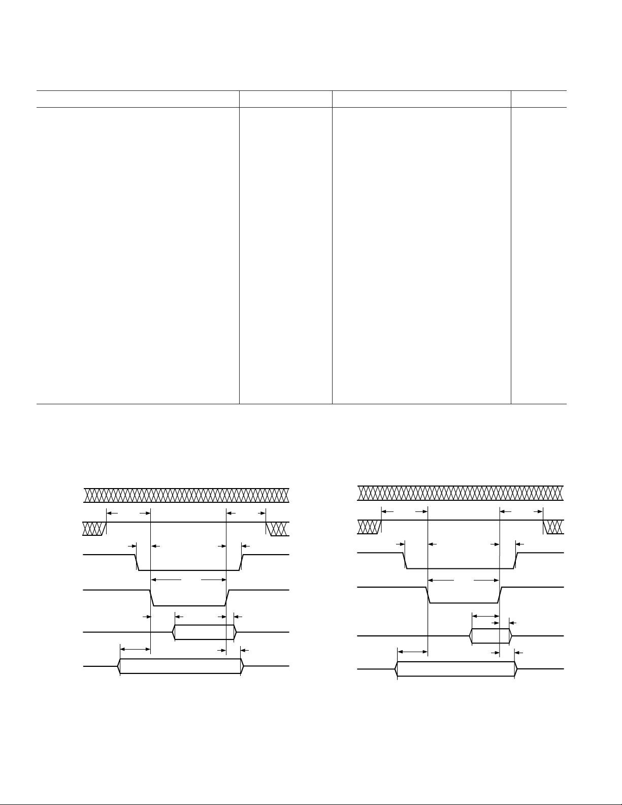
Figure 1. PIO Read Cycle . . . . . . . . . . . . . . . . . . . . . . . . . . . 6
Figure 2. PIO Write Cycle . . . . . . . . . . . . . . . . . . . . . . . . . . 6
Figure 3. DMA Read Cycle . . . . . . . . . . . . . . . . . . . . . . . . . 7
Figure 4. DMA Write Cycle . . . . . . . . . . . . . . . . . . . . . . . . . 7
Figure 5. Codec Transfers . . . . . . . . . . . . . . . . . . . . . . . . . . 7
Figure 6. DSP Port Timing . . . . . . . . . . . . . . . . . . . . . . . . . . 7
Figure 7. I
2
S Serial Port Timing . . . . . . . . . . . . . . . . . . . . . . 7
Figure 8. Reset Pulse Width . . . . . . . . . . . . . . . . . . . . . . . . . 7
Figure 9. Serial Interface Right-Justified Mode . . . . . . . . . . 17
Figure 10. Serial Interface I
2
S-Justified Mode . . . . . . . . . . . 17
Figure 11. Serial Interface Left-Justified Mode . . . . . . . . . . 17
Figure 12. DSP Serial Interface (Default Frame Rate) . . . . 20
Figure 13. DSP Serial Interface (User Programmed
Frame Rate) . . . . . . . . . . . . . . . . . . . . . . . . . . . . . . . . . . . 20
Figure 14. DSP Serial Port . . . . . . . . . . . . . . . . . . . . . . . . . 21
Figure 15. Codec Transfers . . . . . . . . . . . . . . . . . . . . . . . . . 27
Figure 16. Recommended Application Circuit . . . . . . . . . . 48
Figure 17. AD1816A Frequency Response Plots . . . . . . . . . 49
Tables
Table I. DSP Port Time Slot Map . . . . . . . . . . . . . . . . . . . 18
Table II. Chip Register Diagram . . . . . . . . . . . . . . . . . . . . . 21
Table III. Logical Devices and Compatible Plug and
Play Device Drivers . . . . . . . . . . . . . . . . . . . . . . . . . . . . . 22
Table IV. Internal Logical Device Configuration . . . . . . . . 23
Table V. Sound System Direct Registers . . . . . . . . . . . . . . . 23
Table VI. Codec Transfers . . . . . . . . . . . . . . . . . . . . . . . . . 27
Table VII. Indirect Register Map and Reset/Default States . 30
Table VIII. Sound System Indirect Registers . . . . . . . . . . . 31
Table IX. SoundBlaster Pro ISA Bus Registers . . . . . . . . . . 38
Table X. AdLib ISA Bus Registers . . . . . . . . . . . . . . . . . . . 39
Table XI. MIDI ISA Bus Registers . . . . . . . . . . . . . . . . . . . 39
Table XII. Game Port ISA Bus Registers . . . . . . . . . . . . . . 39
Table XIII. AD1816 Pin Muxing . . . . . . . . . . . . . . . . . . . . 45
Table XIV. AD1816A Pin Muxing . . . . . . . . . . . . . . . . . . . 46
–2–
REV. A
Page 3

SPECIFICA TIONS
AD1816A
STANDARD TEST CONDITIONS UNLESS
OTHERWISE NOTED
Temperature 25 °C
Digital Supply (V
Analog Supply (V
Sample Rate (F
Input Signal Frequency 1008 Hz
Audio Output Passband 20 Hz to 20 kHz
V
IH
V
IL
ANALOG INPUT
Parameter Min Typ Max Units
Full-Scale Input Voltage (RMS Values Assume Sine Wave Input)
PHONE_IN, LINE, SYNTH, CD, VID 1 V rms
MIC with +20 dB Gain (MGE = 1) 0.1 V rms
MIC with 0 dB Gain (MGE = 0) 1 V rms
Input Impedance* 17 kΩ
Input Capacitance* 15 pF
) 5.0 V
DD
) 5.0 V
CC
) 48 kHz
S
5.0 V
0V
DAC Test Conditions
0 dB Attenuation
Input Full Scale
16-Bit Linear Mode
100 kΩ Output Load
Mute Off
Measured at Line Output
ADC Test Conditions
0 dB Gain
Input –4 dB Relative to Full Scale
Line Input Selected
16-Bit Linear Mode
2.83 V p-p
0.283 V p-p
2.83 V p-p
PROGRAMMABLE GAIN AMPLIFIER—ADC
Parameter Min Typ Max Units
Step Size (0 dB to 22.5 dB)
(All Steps Tested) 1.5 dB
PGA Gain Range Span 22.5 dB
CD, LINE, MICROPHONE, SYNTHESIZER, AND VIDEO INPUT ANALOG GAIN/ATTENUATORS/MUTE AT LINE OUTPUT
Parameter Min Typ Max Units
CD, LINE, MIC, SYNTH, VID
Step Size: (All Steps Tested)
+12 dB to –34.5 dB 1.5 dB
Input Gain/Attenuation Range 46.5 dB
PHONE_IN
Step Size 0 dB to –45 dB: (All Steps Tested) 3.0 dB
Input Gain/Attenuation Range 45 dB
REV. A
–3–
Page 4

AD1816A
DIGITAL DECIMATION AND INTERPOLATION FILTERS*
Parameter Min Typ Max Units
Audio Passband 0 0.4 × F
S
Hz
Audio Passband Ripple ±0.09 dB
Audio Transition Band 0.4 × F
Audio Stopband 0.6 × F
S
S
0.6 × F
S
Hz
∞ Hz
Audio Stopband Rejection 82 dB
Audio Group Delay 12/F
S
sec
Group Delay Variation Over Passband 0.0 µs
ANALOG-TO-DIGITAL CONVERTERS
Parameter Min Typ Max Units
Resolution 16 Bits
Signal-to-Noise Ratio (SNR) (A-Weighted, Referenced to Full Scale) 82 80 dB
Total Harmonic Distortion (THD) (Referenced to Full Scale) 0.011 0.015 %
–79 –76.5 dB
Audio Dynamic Range (–60 dB Input THD+N Referenced to
Full-Scale, A-Weighted) 79 82 dB
Audio THD+N (Referenced to Full-Scale) 0.019 %
–76 –74.5 dB
Signal-to-Intermodulation Distortion* (CCIF Method) 82 dB
ADC Crosstalk*
Line Inputs (Input L, Ground R, Read R; Input R, Ground L Read L) –95 –80 dB
Line to MIC (Input LINE, Ground and Select MIC, Read ADC) –95 –80 dB
Line to SYNTH –95 –80 dB
Line to CD –95 –80 dB
Line to VID –95 –80 dB
Gain Error (Full-Scale Span Relative to Nominal Input Voltage) ±10 %
Interchannel Gain Mismatch (Difference of Gain Errors) ±1dB
ADC Offset Error –22 +15 mV
DIGITAL-TO-ANALOG CONVERTERS
Parameter Min Typ Max Units
Resolution 16 Bits
Signal-to-Noise Ratio (SNR) (A-Weighted) 83 79 dB
Total Harmonic Distortion (THD) 0.006 0.009 %
–85 –80.5 dB
Audio Dynamic Range (–60 dB Input THD+N Referenced to
Full Scale, A-Weighted) 79 82 dB
Audio THD+N (Referenced to Full Scale) 0.013 0.017 %
–78 –75.5 dB
Signal-to-Intermodulation Distortion* (CCIF Method) 95 dB
Gain Error (Full-Scale Span Relative to Nominal Input Voltage) ±10 %
Interchannel Gain Mismatch (Difference of Gain Errors) ±0.5 dB
DAC Crosstalk* (Input L, Zero R, Measure R_OUT;
Input R, Zero L, Measure L_OUT) –80 dB
Total Out-of-Band Energy (Measured from 0.6 × F
to 100 kHz
S
at L_OUT and R_OUT)* –45 dB
Audible Out-of-Band Energy (Measured from 0.6 × F
to 20 kHz
S
at L_OUT and R_OUT)* –75 dB
MASTER VOLUME ATTENUATORS (L_OUT AND R_OUT, PHONE_OUT)
Parameter Min Typ Max Units
Master Volume Step Size (0 dB to –46.5 dB) 1.5 dB
Master Volume Output Attenuation Range Span 46.5 dB
Mute Attenuation of 0 dB Fundamental* –80 dB
–4–
REV. A
Page 5

AD1816A
DIGITAL MIX ATTENUATORS*
Parameter Min Typ Max Units
2
Step Size: I
Digital Mix Attenuation Range Span 94.8 dB
ANALOG OUTPUT
Parameter Min Typ Max Units
Full-Scale Output Voltage (at L_OUT, R_OUT, PHONE_OUT) 2.8 V p-p
Output Impedance* 570 Ω
External Load Impedance* 10 kΩ
Output Capacitance* 15 pF
External Load Capacitance 100 pF
V
REFX
V
REFX
V
REFX
Master Volume Mute Click (Muted Analog Mixers), Muted
Output Minus Unmuted Output at 0 dB ±5mV
SYSTEM SPECIFICATIONS*
Parameter Min Typ Max Units
System Frequency Response Ripple (Line In to Line Out) 1.0 dB
Differential Nonlinearity ±1 LSB
Phase Linearity Deviation 5 Degrees
S (0), I2S (1), Music, ISA 1.505 dB
* 2.10 2.25 2.40 V
Current Drive* 100 µA
Output Impedance* 6.5 kΩ
STATIC DIGITAL SPECIFICATIONS
Parameter Min Typ Max Units
High Level Input Voltage (V
)2V
IH
XTALI 2.4 V
Low Level Input Voltage (V
High Level Output Voltage (V
Low Level Output Voltage (V
) 0.8 V
IL
), IOH = 8 mA† 2.4 V
OH
), IOL = 8 mA 0.4 V
OL
Input Leakage Current –10 +10 µA
Output Leakage Current –10 +10 µA
POWER SUPPLY
Parameter Min Typ Max Units
Power Supply Range—Analog 4.75 5.25 V
Power Supply Range—Digital 4.75 5.25 V
Power Supply Current 221 mA
Power Dissipation 1105 mW
Analog Supply Current 51 mA
Digital Supply Current 170 mA
Analog Power Supply Current—Power-Down 2 mA
Digital Power Supply Current—Power-Down 24 mA
Analog Power Supply Current—RESET 0.2 mA
Digital Power Supply Current—RESET 10 mA
Power Supply Rejection (100 mV p-p Signal on Both Analog and Digital
Supply Pins, Measured at ADC and Line Outputs) 40 dB
CLOCK SPECIFICATIONS*
Parameter Min Typ Max Units
Input Clock Frequency 33 MHz
Recommended Clock Duty Cycle 25 50 75 %
Power-Up Initialization Time 500 ms
REV. A
–5–
Page 6
AD1816A
TIMING PARAMETERS
(Guaranteed Over Operating Temperature Range)
Parameter Symbol Min Typ Max Units
IOW/IOR Strobe Width t
IOW/IOR Rising to IOW/IOR Falling t
Write Data Setup to IOW Rising t
IOW Falling to Valid Read Data t
AEN Setup to IOW/IOR Falling t
AEN Hold from IOW/IOR Rising t
Adr Setup to IOW/IOR Falling t
Adr Hold from IOW/IOR Rising t
DACK Rising to IOW/IOR Falling t
Data Hold from IOR Rising t
Data Hold from IOW Rising t
DRQ Hold from IOW/IOR Falling t
DACK Hold from IOW/IOR Rising t
Data [SDI] Input Setup Time to SCLK* t
Data [SDI] Input Hold Time from SCLK* t
Frame Sync [SDFS] HI Pulse Width* t
STW
BWDN
WDSU
RDDV
AESU
AEHD
ADSU
ADHD
DKSU
DHD1
DHD2
DRHD
DKHD
S
H
FSW
100 ns
80 ns
10 ns
40 ns
10 ns
0ns
10 ns
0ns
20 ns
2ns
15 ns
25 ns
10 ns
15 ns
10 ns
80 ns
Clock [SCLK] to Frame Sync [SDFS]
Propagation Delay*t
Clock [SCLK] to Output Data [SDO] Valid* t
RESET Pulse Width t
BCLK HI Pulse Width t
BCLK LO Pulse Width t
BCLK Period t
LRCLK Setup t
SDATA Setup t
SDATA Hold t
NOTES
*Guaranteed, not tested.
†All ISA pins MIDI_OUT IOL = 24 mA. Refer to pin description for individual output drive levels.
Specifications subject to change without notice.
PD
DV
RPWL
DBH
DBL
DBP
DLS
DDS
DDH
100 ns
25 ns
25 ns
50 ns
5ns
5ns
5ns
15 ns
15 ns
DRQ (0, 1, 3)
DACK
(0, 1, 3)
PC_D [7:0]
PC_A [15:0]
AEN
IOR
t
DKSU
t
AESU
t
STW
t
RDDV
t
ADSU
Figure 1. PIO Read Cycle
t
DKHD
t
DHD1
t
t
ADHD
AEHD
–6–
DRQ (0, 1, 3)
DACK (0, 1, 3)
AEN
IOW
PC_D [7:0]
PC_A [15:0]
t
DKSU
t
AESU
t
STW
t
WDSU
t
ADSU
Figure 2. PIO Write Cycle
t
DKHD
t
t
DHD2
t
ADHD
AEHD
REV. A
Page 7
DRQ (0, 1, 3)
SCLK
t
PD
t
FSW
t
S
t
H
t
DV
SDFS
SDI
SDO
BIT 15
BIT 14
BIT 0
BIT 15
BIT 14 BIT 0
DACK (0, 1, 3)
AEN
IOR
PC_D [7:0]
t
DKSU
t
RDDV
t
AESU
t
DRHD
t
STW
t
t
AEHD
DKHD
t
AD1816A
DHD1
DRQ (0, 1, 3)
DACK (0, 1, 3)
AEN
IOW
PC_D [7:0]
IOR/IOW
DATA [7:0]
Figure 3. DMA Read Cycle
t
t
AESU
DRHD
t
DKSU
t
Figure 4. DMA Write Cycle
t
BWDN
BYTE N N + 1
STW
t
WDSU
N + 2 N + 3
t
DKHD
t
DHD2
t
AEHD
BCLK
LRCLK
SDATA
LEFT-JUSTIFIED
MODE
SDATA
I2S-JUSTIFIED
MODE
RIGHT-JUSTIFIED
SDATA
MODE
RESET
Figure 6. DSP Port Timing
t
t
DDS
DBH
t
DLS
MSB MSB-1
t
DDH
t
DDS
t
DBP
t
DBL
MSB
t
DDH
t
DDS
MSB
t
DDH
Figure 7. I2S Serial Port Timing
t
RPWL
t
DDS
LSB
t
DDH
Figure 5. Codec Transfers
REV. A
–7–
Figure 8. Reset Pulse Width
Page 8

AD1816A
ABSOLUTE MAXIMUM RATINGS*
Parameter Min Max Units
Power Supplies
Digital (V
Analog (V
) –0.3 6.0 V
DD
) –0.3 6.0 V
CC
Input Current (Except Supply Pins) ±10.0 mA
Analog Input Voltage (Signal Pins) –0.3 V
Digital Input Voltage (Signal Pins) –0.3 V
+ 0.3 V
CC
+ 0.3 V
DD
Ambient Temperature (Operating) 0 +70 °C
Storage Temperature –65 +150 °C
*Stresses greater than those listed under Absolute Maximum Ratings may cause
permanent damage to the device. This is a stress rating only; functional operation
of the device at these or any other conditions above those indicated in the
operational section of this specification is not implied. Exposure to absolute
maximum rating conditions for extended periods may affect device reliability.
ENVIRONMENTAL CONDITIONS
Ambient Temperature Rating:
T
= T
AMB
T
= Case Temperature in °C
CASE
– (PD × θCA)
CASE
PD = Power Dissipation in W
θ
= Thermal Resistance (Case-to-Ambient)
CA
θ
= Thermal Resistance (Junction-to-Ambient)
JA
θ
= Thermal Resistance (Junction-to-Case)
JC
Package u
JA
PQFP 35.1°C/W 7°C/W 28°C/W
TQFP 35.3°C/W 8°C/W 27.3°C/W
ORDERING GUIDE
Temperature Package Package
Model Range Description Option*
AD1816AJS 0°C to +70°C 100-Lead PQFP S-100
AD1816AJST 0°C to +70°C 100-Lead TQFP ST-100
*S = Plastic Quad Flatpack; ST = Thin Quad Flatpack. JST package option
availability subject to 10,000 PC minimum order quantity.
CAUTION
ESD (electrostatic discharge) sensitive device. Electrostatic charges as high as 4000 V readily
accumulate on the human body and test equipment and can discharge without detection.
Although the AD1816A features proprietary ESD protection circuitry, permanent damage may
occur on devices subjected to high energy electrostatic discharges. Therefore, proper ESD
precautions are recommended to avoid performance degradation or loss of functionality.
The AD1816A latchup immunity has been demonstrated at ≥ +100 mA/–80 mA on all pins when
tested to Industry Standard/JEDEC methods.
u
JC
WARNING!
ESD SENSITIVE DEVICE
u
CA
–8–
REV. A
Page 9

2
I
S0_DATA/VOL_UP
2
S0_LRCLK/VOL_DN
I
I2S0_BCLK/GND
PC_A (15)
PC_A (14)
PC_A (13)
PC_A (12)
PC_A (11)
PC_A (10)
PC_A (9)
PC_A (8)
PC_A (7)
PC_A (6)
PC_A (5)
PC_A (4)
PC_A (3)
PC_A (2)
PC_A (1)
PC_A (0)
RESET
RX3D
CX3D
PHONE_OUT
R_OUT
L_OUT
AEN
IOW
IOR
V
GND
AD1816A
PIN CONFIGURATION
100-Lead PQFP
(S-100)
S1_BCLK/MDM_IRQ
S1_LRCLK/MDM_SEL/IRQ (12)/IRQ (13)
DD
SPORT_SCLK/LD_SEL/NC
GND
SPORT_SDFS/LD_DRQ/VOL_UP
SPORT_SDI/LD_IRQ/VOL_DN/GND
SPORT_SDO/LD_DACK/VOL_DN/GND
99989796959493929190898887868584838281
100
1
PIN 1
2
IDENTIFIER
3
4
5
6
7
8
9
10
11
12
13
14
15
16
17
18
19
20
21
22
23
DD
24
25
26
27
28
29
30
V
PC_D (0)
PC_D (2)
PC_D (1)
AD1816A
(Not to Scale)
GND
PC_D (3)
TOP VIEW
DD
V
PC_D (5)
PC_D (4)
PC_D (7)
PC_D (6)
S1_DATA/IRQ (3)/IRQ (9)
2
2
2
I
I
I
GND
80
IRQ (5)
79
IRQ (7)
78
IRQ (9)/IRQ (14)
77
IRQ (10)/IRQ (4)
76
IRQ (11)/IRQ (9)/IRQ (4)
75
IRQ (15)/IRQ (11)
74
DRQ (0)
73
DRQ (1)
72
DRQ (3)
71
V
DD
70
GND
69
XCTL1/RING/LD_SEL1
68
XCTL0/PCLKO/PNPRST
67
MIDI_OUT
66
MIDI_IN
65
GND
64
XTALO
63
XTALI
62
V
DD
61
DACK (0)
60
DACK (1)
59
DACK (3)
58
EE_CLK/GND
57
EE_DATA/GND
56
B_X
55
B_Y
54
A_X
53
A_Y
52
B_1
51
B_2
REV. A
NC = NO CONNECT
32
31
L_VID
R_VID
34
35
38
37
39
L_FILT
R_FILT
40
41
R_LINE
L_AAFILT
R_AAFILT
42
43
L_LINE
PHONE_IN
44
45
MIC
R_SYNTH
36
33
CC
REF
V
V
REF_X
GNDA
V
48
47
46
L_CD
R_CD
L_SYNTH
49
A_2
50
A_1
–9–
Page 10

AD1816A
PIN CONFIGURATION
100-Lead TQFP
(ST-100)
2
I
S0_BCLK/GND
PC_A (15)
PC_A (14)
PC_A (13)
PC_A (12)
PC_A (11)
PC_A (10)
PC_A (9)
PC_A (8)
PC_A (7)
PC_A (6)
PC_A (5)
PC_A (4)
PC_A (3)
PC_A (2)
PC_A (1)
PC_A (0)
RESET
RX3D
CX3D
AEN
IOW
IOR
V
GND
S0_DATA/ VOL_UP
S0_LRCLK/ VOL_DN
2
2
I
SPORT_SDI/ LD_IRQ /VOL_DN /GND
I
SPORT_SDO/ LD_DACK / VOL_DN /GND
9998979695949392919089888786858483828180797877
100
1
PIN 1
2
IDENTIFIER
3
4
5
6
7
8
9
10
11
12
13
14
15
16
17
18
19
20
21
DD
22
23
24
25
27
28
29
26
R_VID
L_OUT
R_OUT
PHONE_OUT
SPORT_SCLK/LD_SEL /NC
SPORT_SDFS/ LD_DRQ /VOL_UP
30
31
CC
V
L_VID
V
GND
33
32
REF
V
GNDA
DD
PC_D (1)
PC_D (0)
34
35
REF_X
V
R_FILT
V
GND
PC_D (3)
PC_D (2)
AD1816A
TOP VIEW
(Not to Scale)
36
37
38
39
L_FILT
R_LINE
L_AAFILT
R_AAFILT
DD
PC_D (4)
40
L_LINE
PC_D (6)
PC_D (5)
PC_D (7)
41
42
43
MIC
R_SYNTH
PHONE_IN
S1_LRCLK/MDM_SEL/IRQ (12)/IRQ (13)
S1_DATA/IRQ (3)/IRQ (9)
S1_BCLK/MDM_IRQ
2
2
2
GND
I
I
I
44
45
46
47
A_2
L_CD
R_CD
L_SYNTH
IRQ (5)
IRQ (7)
48
49
A_1
B_2
IRQ (9)/IRQ (14)
76
75
IRQ (10)/IRQ (4)
74
IRQ (11)/IRQ (9)/IRQ (4)
73
IRQ (15)/IRQ (11)
72
DRQ (0)
71
DRQ (1)
DRQ (3)
70
69
V
DD
68
GND
67
XCTL1/RING/LD_SEL1
XCTL0/PCLKO/PNPRST
66
65
MIDI_OUT
64
MIDI_IN
63
GND
62
XTALO
61
XTALI
60
V
DD
59
DACK (0)
58
DACK (1)
57
DACK (3)
56
EE_CLK/GND
55
EE_DATA/GND
54
B_X
53
B_Y
52
A_X
51
A_Y
50
B_1
NC = NO CONNECT
–10–
REV. A
Page 11

AD1816A
PIN FUNCTION DESCRIPTIONS
Analog Signals (All Inputs must be AC-Coupled)
Pin Name PQFP TQFP I/O Description
MIC 44 42 I Microphone Input. The MIC input may be either line-level or –20 dB from line-level (the
difference being made up through a software controlled 20 dB gain block). The mono MIC
input may be sent to the left and right channel of the ADC for conversion, or gained/
attenuated from +12 dB to –34.5 dB in 1.5 dB steps and then summed with left and right
line OUT before the Master Volume stage.
L_LINE 42 40 I Left Line-Level Input. The left line-level input may be sent to the left channel of the ADC;
gained/attenuated from +12 dB to –34.5 dB in 1.5 dB steps and then summed with left line
OUT (L_OUT).
R_LINE 41 39 I Right Line-Level Input. The right line-level input may be sent to the right channel of the
ADC; gained/attenuated from +12 dB to –34.5 dB in 1.5 dB steps and then summed with
right line OUT (R_OUT).
L_SYNTH 46 44 I Left Synthesizer Input. The left MIDI upgrade line-level input may be sent to the left
channel of the ADC; gained/attenuated from +12 dB to –34.5 dB in 1.5 dB steps and then
summed with left line OUT (L_OUT).
R_SYNTH 45 43 I Right Synthesizer Input. The right MIDI upgrade line-level input may be sent to the right
channel of the ADC; gained/attenuated from +12 dB to –34.5 dB in 1.5 dB steps and then
summed with right line OUT (R_OUT).
L_CD 48 46 I Left CD Line-Level Input. The left CD line-level input may be sent to the left channel of
the ADC; gained/attenuated from +12 dB to –34.5 dB in 1.5 dB steps and then summed
with left line OUT (L_OUT).
R_CD 47 45 I Right CD Line-Level Input. The right CD line-level input may be sent to the right channel
of the ADC; gained/attenuated from +12 dB to –34.5 dB in 1.5 dB steps and then summed
with right line OUT (R_OUT).
L_VID 32 30 I Left Video Input. The left audio track for a video line-level input may be sent to the left
channel of the ADC; gained/attenuated from +12 dB to –34.5 dB in 1.5 dB steps and then
summed with left line OUT (L_OUT).
R_VID 31 29 I Right Video Input. The right audio track for a video line-level input may be sent to the
right channel of the ADC; gained/attenuated from +12 dB to –34.5 dB in 1.5 dB steps and
then summed with right line OUT (R_OUT).
L_OUT 30 28 O Left Output. Left channel line-level post-mixed output. The final stage passes through the
Master Volume block and may be attenuated 0 dB to –45 dB in 1.5 dB steps.
R_OUT 29 27 O Right Output. Right channel line-level post-mixed output. The final stage passes through
the Master Volume block and may be attenuated 0 dB to –45 dB in 1.5 dB steps.
PHONE_IN 43 41 I Phone Input. Line-level input from a DAA/modem chipset.
PHONE_OUT 28 26 O Phone Output. Line-level output from a DAA/modem chipset.
RX3D 26 24 O Phat Stereo Phase Expander filter network, resistor pin.
CX3D 27 25 I Phat Stereo Phase Expander filter network, capacitor pin.
REV. A
–11–
Page 12

AD1816A
Parallel Interface (All Outputs are 24 mA Drivers)
Pin Name PQFP TQFP I/O Description
PC_D[7:0] 85–88, 91–94 83–86, 89–92 I/O Bidirectional ISA Bus PC Data, 24 mA drive. Connects the AD1816A to
the low byte data on the bus.
IRQ (x)* 75–81, 83 73–79, 81 O Host Interrupt Request, 24 mA drive. IRQ (3)/IRQ (9), IRQ (5), IRQ (7),
IRQ (9)/IRQ (14), IRQ (10)/IRQ (4), IRQ (11)/IRQ (9)/IRQ (4), IRQ (12)/
IRQ (13), IRQ (15)/IRQ (11). Active HI signals indicating a pending interrupt.
DRQ (x) 72–74 70–72 O DMA Request, 24 mA drive. DRQ (0), DRQ (1), DRQ (3). Active HI sig-
nals indicating a request for DMA bus operation.
PC_A[15:0] 4–19 2–17 I ISA Bus PC Address. Connects the AD1816A to the ISA bus address lines.
AEN 20 18 I Address Enable. Low signal indicates a PIO transfer.
DACK (x) 59–61 57–59 I DMA Acknowledge. DACK (0), DACK (1), DACK (3). Active LO signal
indicating that a DMA operation can begin.
IOR 22 20 I I/O Read. Active LO signal indicates a read operation.
IOW 21 19 I I/O Write. Active HI signal indicates a write operation.
RESET 25 23 I Reset. Active HI.
Game Port
Pin Name PQFP TQFP I/O Description
A_1 50 48 I Game Port A, Button #1.
A_2 49 47 I Game Port A, Button #2.
A_X 54 52 I Game Port A, X-Axis.
A_Y 53 51 I Game Port A, Y-Axis.
B_1 52 50 I Game Port B, Button #1.
B_2 51 49 I Game Port B, Button #2.
B_X 56 54 I Game Port B, X-Axis.
B_Y 55 53 I Game Port B, Y-Axis.
MIDI Interface Signal (24 mA Drivers)
Pin Name PQFP TQFP I/O Description
MIDI_IN 66 64 I RXD MIDI Input. This pin is typically connected to Pin 15 of the game
port connector.
MIDI_OUT 67 65 O TXD MIDI Output. This pin is typically connected to Pin 12 of the game
port connector.
–12–
REV. A
Page 13

Muxed Serial Ports (8 mA Drivers)
Pin Name PQFP TQFP I/O Description
2
I
S(0)_BCLK* 3 1 I I2S (0) Bit Clock.
2
I
S(0)_LRCLK* 2 100 I I2S (0) Left/Right Clock.
2
S(0)_DATA* 1 99 I I2S (0) Serial Data Input.
I
2
S(1)_BCLK* 82 80 I I2S (1) Bit Clock.
I
2
I
S(1)_LRCLK* 83 81 I I2S (1) Left/Right Clock.
2
S(1)_DATA* 81 79 I I2S (1) Serial Data Input.
I
SPORT_SDI* 100 98 I Serial Port Digital Serial Input.
SPORT_SCLK* 97 95 O Serial Port Serial Clock.
SPORT_SDFS* 98 96 O Serial Port Serial Data Frame Synchronization.
SPORT_SDO* 99 97 O Serial Port Serial Data Output.
Miscellaneous Analog Pins
Pin Name PQFP TQFP I/O Description
AD1816A
V
REF_X
V
REF
36 34 O Voltage Reference. Nominal 2.25 volt reference available for dc-coupling
and level-shifting. V
V
should be bypassed with 10 µF and 0.1 µF parallel capacitors.
REF_X
should not be used to sink or source signal current.
REF_X
35 33 I Voltage Reference Filter. Voltage reference filter point for external bypassing
only. V
should be bypassed with 10 µF and 0.1 µF parallel capacitors.
REF
L_FILT 38 36 I Left Channel Filter. Requires a 1.0 µF to analog ground for proper
operation.
R_FILT 37 35 I Right Channel Filter. Requires a 1.0 µF to analog ground for proper
operation.
L_AAFILT 40 38 I Left Channel Antialias Filter. This pin requires a 560 pF NPO
capacitor to analog ground for proper operation.
R_AAFILT 39 37 I Right Channel Antialias Filter. This pin requires a 560 pF NPO
capacitor to analog ground for proper operation.
Crystal Pin
Pin Name PQFP TQFP I/O Description
XTALO 64 62 O 33 MHz Crystal Output. If no Crystal is present leave XTALO
unconnected.
XTALI 63 61 I 33 MHz Clock. When using a crystal as a clock source, the crystal should
be connected between the XTALI and XTALO pins. Clock input may
be driven into XTALI in place of a crystal. When using an external clock,
V
must be 2.4 V rather than the VIH of 2.0 V specified for all other
IH
digital inputs.
External Logical Devices
Pin Name PQFP TQFP I/O Description
LD_IRQ* 100 98 I Logical Device IRQ.
LD_DACK* 99 97 O Logical Device DACK.
LD_DRQ* 98 96 I Logical Device DRQ.
LD_SEL* 97 95 O Logical Device Select.
MDM_SEL* 83 81 O Modem Chip Set Select.
MDM_IRQ* 82 82 I Modem Chip Set IRQ.
LD_SEL1* 69 67 O Logical Device (1) Select.
PNPRST* 68 66 O Plug and Play Reset.
REV. A
–13–
Page 14

AD1816A
Hardware Volume Pins
Pin Name PQFP TQFP I/O Description
VOL_DN* 2, 99, 100 97, 98, 100 I Master Volume Down. Modifies output level on pins L_OUT and R_OUT.
When asserted LO, decreases Master Volume by 1.5 dB/sec. Must be asserted at
least 25 ms to be recognized. When asserted simultaneously with
put is muted. Output level modification reflected in indirect register [41].
VOL_UP* 1, 98 96, 99 I Master Volume Up. Modifies output level on pins L_OUT and R_OUT. When
asserted LO, increases Master Volume by 1.5 dB/sec. Must be asserted at least
25 ms to be recognized. When asserted simultaneously with
muted. Output level modification reflected in indirect register [41].
Control Pins
Pin Name PQFP TQFP I/O Description
XCTL0* 68 66 O External Control 0. The state of this pin (TTL HI or LO) is reflected in codec
indexed register. This pin is an open drain driver.
PCLKO* 68 66 O Programmable Clock Output. This pin can be programmed to generate an out-
put clock equal to F
, 8 × FS, 16 × FS, 32 × FS, 64 × FS, 128 × FS or 256 × FS.
S
MPEG decoders typically require a master clock of 256 × F
synchronization.
XCTL1* 69 67 O External Control 1. The state of this pin (TTL HI or LO) is reflected in codec
indexed register. Open drain, 8 mA active 0.5 mA pull-up resistor.
RING* 69 67 I Ring Indicator. Used to accept the ring indicator flag from the DAA.
VOL_UP, out-
VOL_UP, output is
for audio
S
Power Supplies
Pin Name PQFP TQFP I/O Description
V
CC
33 31 I Analog Supply Voltage (+5 V).
GNDA 34 32 I Analog Ground.
V
DD
23, 62, 71, 21, 60, 69, I Digital Supply Voltage (+5 V).
89, 95 87, 93
GND 3*, 24, 65, 1*, 22, 63, I Digital Ground.
70, 84, 90, 68, 82, 88,
96, 99*, 100* 94, 97*, 98*
Optional EEPROM Pins
Pin Name PQFP TQFP I/O Description
EE_CLK 58 56 O EEPROM Clock. Open drain output, requires external pull-up.
EE_DATA 57 55 I/O EEPROM Data. Open drain I/O, requires external pull-up.
*The position of this pin location/function is dependent on the EEPROM data.
–14–
REV. A
Page 15

AD1816A
HOST INTERFACE
The AD1816A contains all necessary ISA bus interface logic on
chip. This logic includes address decoding for all onboard
resources, control and signal interpretation, DMA selection and
control logic, IRQ selection and control logic, and all interface
configuration logic.
The AD1816A supports a Type “F” DMA request/grant architecture for transferring data with the ISA bus through the 8-bit
interface. The AD1816A also supports DACK preemption. Programmed I/O (PIO) mode is also supported for control register
accesses and for applications lacking DMA control. The
AD1816A includes dual DMA count registers for full-duplex
operation enabling simultaneous capture and playback on separate DMA channels.
Codec Functional Description
The AD1816A’s full-duplex stereo codec supports business audio
and multimedia applications. The codec includes stereo audio
converters, complete on-chip filtering, MPC Level-2 and
Level-3 compliant analog mixing, programmable gain and attenuation, variable sample rate converters, extensive digital mixing
and FIFOs buffering the Plug and Play ISA bus interface.
Analog Inputs
The codec contains a stereo pair of ∑∆ analog-to-digital converters (ADC). Inputs to the ADC can be selected from the following analog signals: mono (PHONE_IN), mono microphone
(MIC), stereo line (LINE), external stereo synthesizer
(SYNTH), stereo CD ROM (CD), stereo audio from a video
source (VID) and post-mixed stereo or mono line output (OUT).
Analog Mixing
PHONE_IN, MIC, LINE, SYNTH, CD and VID can be mixed
in the analog domain with the stereo line OUT from the Σ∆
digital-to-analog converters (DAC). Each channel of the stereo
analog inputs can be independently gained or attenuated from
+12 dB to –34.5 dB in 1.5 dB steps, except for PHONE_IN,
which has a range of 0 dB to –45 dB steps. The summing path
for the mono inputs (MIC, and PHONE_IN to line OUT) duplicates mono channel data on both the left and right line OUT,
which can also be gained or attenuated from +12dB to –34.5 dB
in 1.5 dB steps for MIC, and +0 dB to –45.0 dB in 3 dB steps
for PHONE_IN. The left and right mono summing signals are
always identical being gained or attenuated equally.
Analog-to-Digital Datapath
The selector sends left and right channel information to the programmable gain amplifier (PGA). The PGA following the selector allows independent gain for each channel entering the ADC
from 0 dB to 22.5 dB in 1.5 dB steps.
For supporting time correlated I/O echo cancellation, the ADC
is capable of sampling microphone data on the left channel and
the mono summation of left and right OUT on the right channel.
The codec can operate in either a global stereo mode or a global
mono mode with left channel inputs appearing at both channels of
the 16-bit Σ∆ converters. Data can be sampled at the programmed
sampling frequency (from 4 kHz to 55.2 kHz with 1 Hz resolution).
Digital Mixing and Sample Rates
The audio ADC sample rate and the audio DAC sample rates
are completely independent. The AD1816A includes a variable
sample rate converter that lets the codec instantaneously change
and process sample rates from 4 kHz to 55.2 kHz with a resolution of 1 Hz. The in-band integrated noise and distortion
artifacts introduced by rate conversions are below –90 dB.
REV. A
–15–
Up to four channels of digital data can be summed together and
presented to the stereo DAC for conversion. Each digital channel pair can contain information encoded at a different sample
rate. For example, 8 kHz .wav data received from the ISA interface, 48 kHz MPEG audio data received from I
44.1 kHz CD data received from I
2
S(1) and internally generated
2
S(0), digital
22.05 kHz music data may be summed together and converted
by the DACs.
Digital-to-Analog Datapath
The internally generated music synthesizer data, PCM data
received from the ISA interface, data received from the I
port and data received from the I
2
S(1) port, and the DSP serial
2
S(0)
port passes through an attenuation mute stage. The attenuator
allows independent control over each digital channel, which can
be attenuated from 0 dB to –94.5 dB in 1.5 dB steps before being summed together and passed to the DAC, or the channel
may be muted entirely.
Analog Outputs and Phat Stereo
The analog output of the DAC can be summed with any of the
analog input signals. The summed analog signal enters the
Master Volume stage where each channel L_OUT, R_OUT and
PHONE_OUT may be attenuated from 0 dB to –46.5 dB in
1.5 dB steps or muted.
Analog Outputs and Phat Stereo
The AD1816A includes ADI’s proprietary Phat Stereo 3D
phase enhancement technology, which creates an increased
sense of spaciousness using two speakers. Our unique patented
feedback technology enables superior control over the width and
depth of the acoustic signals arriving at the human ear. The
AD1816A employs an electrical model of the speaker-to-ear
path allowing precise control over a signal’s phase at the ear. The
Phat Stereo circuitry expands apparent sound images beyond the
angle of the speakers by exploiting phase information in the audio
signal and creating a more immersive listening experience.
Digital Data Types
The codec can process 16-bit twos complement PCM linear
digital data, 8-bit unsigned magnitude PCM linear data and
8-bit µ-law or A-law companded digital data as specified in the
control registers. The AD1816A also supports ADPCM encoded in the Creative SoundBlaster ADPCM formats.
Host-Based Echo Cancellation Support
The AD1816A supports time correlated I/O data format by presenting MIC data on the left channel of the ADC and the mono
summation of left and right OUT on the right channel. The
ADC sample rates are independent of the DAC sample rate allowing the AD1816A to support ADC time correlated I/O data at
8 kHz and DAC data at any other sample rate in the range of
4 kHz to 55.2 kHz simultaneously.
Telephony Support
The AD1816A contains a PHONE_IN input and a
PHONE_OUT output. These pins are supplied so the AD1816A
may be connected to a modem chip set, a telephone handset or
down-line phone.
WSS and SoundBlaster Compatibility
Windows Sound System software audio compatibility is built
into the AD1816A.
SoundBlaster emulation is provided through the SoundBlaster
register set and the internal music synthesizer. SoundBlaster Pro
version 3.02 functions are supported, including record and Creative SoundBlaster ADPCM.
Page 16

AD1816A
Virtually all applications developed for SoundBlaster, Windows
Sound System, AdLib and MIDI MPU-401 platforms run on the
AD1816A SoundPort Controller. Follow the same development
process for the controller as you would for these other devices.
As the AD1816A contains SoundBlaster (compatible) and
Windows Sound System logical devices. You may find the
following related development kits useful when developing
AD1816A applications.
Developer Kit for SoundBlaster Series, 2nd ed. © 1993,
Creative Labs, Inc., 1901 McCarthy Blvd., Milpitas, CA 95035
Microsoft Windows Sound System Driver Development Kit (CD),
Version 2.0, © 1993, Microsoft Corp., One Microsoft Way,
Redmond, WA 98052
The following reference texts can serve as additional sources of information on developing applications that run on the AD1816A.
S. De Furia & J. Scacciaferro, The MIDI Implementation Book,
(© 1986, Third Earth, Pompton Lake)
C. Petzold, Programming Windows: the Microsoft guide to writ-
ing applications for Windows 3.1, 3rd. ed., (© 1992, Microsoft
Press, Redmond)
K. Pohlmann, Principles of Digital Audio, (© 1989, Sams,
Indianapolis)
A. Stolz, The SoundBlaster Book, (© 1993, Abacaus, Grand
Rapids)
J. Strawn, Digital Audio Engineering, An Anthology, (© 1985,
Kaufmann, Los Altos)
Yamamoto, MIDI Guidebook, 4th. ed., (© 1987, 1989,
Roland Corp.)
Multimedia PC Capabilities
The AD1816A is MPC-2 and MPC-3 compliant. This compliance is achieved through the AD1816A’s flexible mixer and the
embedded chip resources.
Music Synthesis
The AD1816A includes an embedded music synthesizer that
emulates industry standard OPL3 FM synthesizer chips and
delivers 20 voice polyphony. The internal synthesizer generates
digital music data at 22.05 kHz and is summed into the DACs
digital data stream prior to conversion. To sum synthesizer data
with the ADC output, the ADC must be programmed for a
22.05 kHz sample rate.
The synthesizer is a hardware
implementation of Eusynth-1+
code that was developed by
EUP
HONICS
Euphonics, a research and development company that specializes
in audio processing and electronic
music synthesis.
EuSynth-1+
Wavetable MIDI Inputs
The AD1816A has a dedicated analog input for receiving an
analog wavetable synthesizer output. Alternatively, a wavetable
synthesizer’s I
nected to one of the AD1816A’s I
table data from the AD1816A’s I
other digital data streams being handled by the AD1816A and
then sent to the 16-bit Σ∆ DAC.
2
S formatted digital output can be directly con-
2
S serial ports. Digital wave-
2
S port may be summed with
MIDI
The primary interface for communicating MIDI data to and from
the host PC is the compatible MPU-401 interface that operates
only in UART mode. The MPU-401 interface has two built-in
FIFOs: a 64-byte receive FIFO and a 16-byte transmit FIFO.
Game Port
An IBM-compatible game port interface is provided on chip.
The game port supports up to two joysticks via a 15-pin D-sub
connector. Joystick registers supporting the Microsoft Direct
Input standard are included as part of the codec register map.
The AD1816A may be programmed to automatically sample the
game port and save the value in the Joystick Position Data Register. When enabled, this feature saves up to 10% CPU MIPS
by off-loading the host from constantly polling the joystick port.
Volume Control
The registers that control the Master Volume output stage are
accessible through the ISA Bus. Master Volume output can also
be controlled through a 2-pin hardware interface. One pin is
used to increase the gain, the other pin attenuates the output
and both pins together entirely mute the output. Once muted, any
further activity on these pins will unmute the AD1816A’s output.
Plug and Play Configuration
The AD1816A is fully Plug and Play configurable. For motherboard applications, the built-in Plug and Play protocol can be
disabled with a software key providing a back door for the BIOS
to configure the AD1816A’s logical devices. For information on
the Plug and Play mode configuration process, see the Plug and
Play ISA Specification Version 1.0a (May 5, 1994). All the
AD1816A’s logical devices comply with Plug and Play resource
definitions described in the specification.
The AD1816A may alternatively be configured using an optional
Plug and Play Resource ROM. When the EEPROM is present,
some additional AD1816A muxed-pin features become available. For example, pins that control an external modem logical
device are muxed with the DSP serial port. Some of these pin
option combinations are mutually exclusive (see Appendix A for
more information).
REFERENCES
The AD1816A also complies with the following related specifications; they can be used as an additional reference to AD1816A
operations beyond the material in this data sheet.
Plug and Play ISA Specification, Version 1.0a, © 1993, 1994,
Intel Corp. & Microsoft Corp., One Microsoft Way,
Redmond, WA 98052
Multimedia PC Level 2 Specification, © 1993, Multimedia PC
Marketing Council, 1730 M St. NW, Suite 707, Washington,
DC 20036
MIDI 1.0 Detailed Specification & Standard MIDI Files 1.0,
© 1994, MIDI Manufacturers Association, PO Box 3173
La Habra, CA 90632-3173
Recommendation G.711-Pulse Code Modulation (PCM) Of Voice
Frequencies (µ-Law & A-Law Companding), The International
Telegraph and Telephone Consultative Committee IX Plenary
Assembly Blue Book, Volume III - Fascicle III.4, General
Aspects Of Digital Transmission Systems; Terminal
Equipment’s, Recommendations G.700 - G.795, (Geneva,
1988), ISBN 92-61-03341-5
–16–
REV. A
Page 17

AD1816A
SERIAL INTERFACES
2
S Serial Ports
I
The two I2S serial ports on the AD1816A accept serial data in the following formats: Right-Justified, I2S-Justified and Left-Justified.
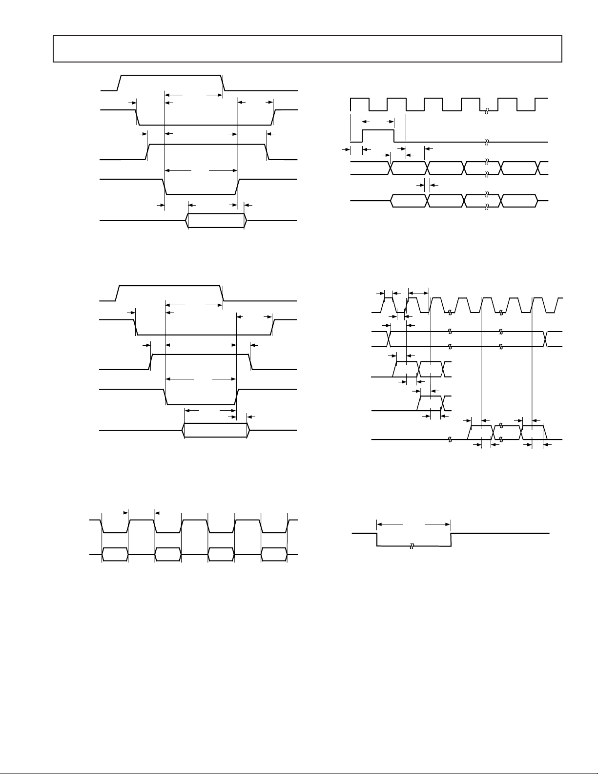
Figure 9 shows the right-justified mode. LRCLK is HI for the left channel and LO for the right channel. Data is valid on the rising
edge of the BCLK. The MSB is delayed 16-bit clock periods from an LRCLK transition, so that when there are 64 BCLK periods
per LRCLK period, the LSB of the data will be right-justified to the next LRCLK transition.
LRCLK
BCLK
SDATA 15 14 13 12 11 10 9 8 7 6 5 4 3 2 1 0
LEFT CHANNEL
14 13 12 11 10 9 8 7 6 5 4 3 2 1 015
RIGHT CHANNEL
Figure 9. Serial Interface Right-Justified Mode
Figure 10 shows the I2S-justified mode. LRCLK is LO for the left channel and HI for the right channel. Data is valid on the rising
edge of BCLK. The MSB is left-justified to an LRCLK transition, but with a single BCLK period delay.
LRCLK
BCLK
SDATA
15 14 13 12 11 10 9 8 7 6 5 4 3 2 1 0
LEFT CHANNEL
RIGHT CHANNEL
1413121110987654321015
Figure 10. Serial Interface I2S-Justified Mode
Figure 11 shows the left-justified mode. LRCLK is HI for the left channel and LO for the right channel. Data is valid on the rising
edge of BCLK. The MSB is left-justified to an LRCLK transition, with no MSB delay.
LRCLK
BCLK
SDATA
LEFT CHANNEL
15 14 13 12 11 10 9 8 7 6 5 4 3 2 1 0
1413121110987654321015
RIGHT CHANNEL
Figure 11. Serial Interface Left-Justified Mode
Bidirectional DSP Serial Interface
The AD1816A SoundPort Controller transmits and receives both data and control/status information through its DSP serial interface
port (SPORT). The AD1816A is always the bus master and supplies the frame sync and the serial clock. The AD1816A has four
pins assigned to the SPORT: SDI, SDO, SDFS and SCLK. The SPORT has two operating modes: monitor and intercept. The
SPORT always monitors the various data streams being processed by the AD1816A. In intercept mode, any of the digital data
streams can be manipulated by the DSP before reaching the final ADC or DAC stages.
The SDI and SDO pins handle the serial data input and output of the AD1816A. Communication in and out of the AD1816A requires
that bits of data be transmitted after a rising edge of SCLK and sampled on the falling edge of SCLK. The SCLK frequency is
always 11 MHz (or 1/3 or XTALI).
DSP Serial Port Interface time slots are mapped as shown in Table I.
REV. A
–17–
Page 18

AD1816A
Table I. DSP Port Time Slot Map
Time Slot SDI Pin SDO Pin
0 Control Word Input Status Word Output
1 Control Register Data Input Control Register Data Output
2 * SS/SB ADC Right Input (to ISA) SS/SB ADC Right Output (from Codec)
3 * SS/SB ADC Left Input (to ISA) SS/SB ADC Left Output (from Codec)
4 * SS/SB DAC Right Input (to Codec) SS/SB DAC Right Output (from ISA)
5 * SS/SB DAC Left Input (to Codec) SS/SB DAC Left Output (from ISA)
6 * FM DAC Right Input (to Codec) FM DAC Right Output (from FM Synth Block)
7 * FM DAC Left Input (to Codec) FM DAC Left Output (from FM Synth Block)
8* I
9* I
10 * I
11 * I2S (0) DAC Left Input (to Codec) I2S (0) DAC Left Output (from I2S Port (0))
*This data is ignored by the AD1816A unless the channel pair is in intercept mode (see below).
SS = Sound System Mode
SB = SoundBlaster Mode
At start-up (after pin reset), there are exactly 12 time slots per frame. The frame rate will be 57,291 and 2/3 Hz (11MHz sclk/
[16 bits × 12 slots]). Interfacing with an Analog Devices 21xx family DSP can be achieved by putting the ADSP-21xx in 24 slot per
frame mode, where the first 12 and second 12 slots in the ADSP-21xx frame are identical.
The frame rate can be changed from its default by a write to the DFS(2:0) bits in register 33. Rate choices are: Maximum (57,291
and 2/3 Hz default), SS capture rate, SS playback rate, FM rate, I
than 57,261 and 2/3 Hz, extra SCLK periods are added to fill up the time. The number of SCLK periods added will vary somewhat
from frame to frame.
To control the sample data flow of each channel through the DSP Port, valid input, valid output and request bits are located in the
control and status words. If the specified channel sample rate is equal to the frame rate, these bits may be ignored since they will
always be set to “1.”
By default, the DSP serial port allows only codec sample data I/O to be monitored. Intercept modes must be enabled to make substitutions in sample data flow to and from the codec. There are five bits in SS register 33, which enable intercept mode for SS capture,
SS playback, FM playback, I
Control Word Input (Slot 0 SDI)
2
S (1) DAC Right Input (to Codec) I2S (1) DAC Right Output (from I2S Port (1))
2
S (1) DAC Left Input (to Codec) I2S (1) DAC Left Output (from I2S Port (1))
2
S (0) DAC Right Input (to Codec) I2S (0) DAC Right Output (from I2S Port (0))
2
S Port (1) rate, or I2S Port (0) rate. When the frame rate is less
2
S Port (1) playback and I2S Port (0) playback.
15 14 13 12 11 10 9 8
FCLR RES RES SSCVI SSPVI FMVI IS1VI IS0VI
76543210
ALIVE R/W IA[5:0]
IA [5:0] Indirect Register Address. Sound System Indirect Register Address defines the address of indirect registers shown
in Table VI.
R/W Read/Write request. Either a read from or a write to an SS indirect register occurs every frame. Setting this bit ini-
tiates an SS indirect register read while clearing this bit initiates an SS indirect register write.
ALIVE DSP port alive bit. When set, this bit indicates to the power-down timer that the DSP port is active. When cleared,
this bit indicates that the DSP port is inactive.
IS0VI I
2
S Port 0 Substitution Data Input Valid Flag. This bit is ignored if: (1) Intercept mode is not enabled for the I
port 0 channel pair, or (2) The AD1816A did not request data from the I
frame. Otherwise, setting this bit indicates that slots 10 and 11 contain valid right and left I
2
S port 0 channel pair in the previous
2
S Port 0 substitution
2
S
data. When this bit is cleared, data in slots 10 and 11 is ignored.
IS1VI I
2
S Port 1 Substitution Data Input Valid Flag. This bit is ignored if: (1) Intercept mode is not enabled for I
1 channel pair or (2) The AD1816A did not request data from the I
Otherwise, setting this bit indicates that Slots 8 and 9 contain valid right and left I
2
S port channel pair in the previous frame.
2
S Port 1 substitution data.
2
S port
When this bit is cleared, data in slots 8 and 9 is ignored.
FMVI FM Synthesis Substitution Data Input Valid Flag. This bit is ignored if: (1) Intercept mode is not enabled for the
FM synthesis channel pair or (2) The AD1816A did not request data from the FM synthesis channel pair in the
previous frame (see the FMRQ Bit 9 in the status word output). Otherwise, setting this bit to 1 indicates that slots
6 and 7 contain valid right and left FM synthesis channel substitution data. When this bit is reset to 0, data in slots
6 and 7 is ignored.
–18–
REV. A
Page 19

AD1816A
SSPVI SS/SB Playback Substitution Data Input Valid Flag. This bit is ignored if: (1) Intercept mode is not enabled for
SS/SB playback or (2) The AD1816A did not request data for SS/SB playback in the previous frame (see the
SSPRQ bit in the Status Word Output). Otherwise, setting this bit indicates that Slots 4 and 5 contain valid right
and left SS/SB playback substitution data. If in “capture rate equal to playback rate” mode, setting this bit also indicates that valid capture substitution data is being sent to the AD1816A. If not in modem mode, right and left
channel capture substitution data is accepted in Slots 2 and 3 respectively. If in modem mode, only mono capture
substitution data is accepted in slots 2 and 3. When this bit is cleared, data in all slots controlled by this bit, as defined above, is ignored.
SSCVI SS/SB Capture Substitution Data Input Valid Flag. This bit is ignored if: (1) Intercept mode is not enabled for SS/
SB capture or (2) The AD1816A did not request data for SS/SB capture in the previous frame (see the SSCRQ
bit in the Status Word Output). Otherwise, setting this bit indicates that valid SS/SB capture substitution data is
being sent to the AD1816A. If not in modem mode, or DSP port or ISA bus based, right and left channel capture
data is accepted in Slots 2 and 3 respectively. If in modem mode, only mono capture substitution data is accepted
in Slot 3, because Slot 2, which is mapped to the right capture channel, is being used for modem. This mono data
will, however, be sent to both left and right ISA SS/SB capture channels. When this bit is cleared, data in Slots 3
and 2 is ignored.
RES Reserved: To ensure future compatibility write “0” to all reserved bits.
FCLR DSP Port Clear Status Flag. When this bit is set, (write 1), the PNPR and PDN flag bits in the status word (Bits
15 and 14 of slots 0 SDO) are cleared. When this bit is cleared, (writing a 0), it has no effect on PNPR and PDN
and preserves them in the previous states.
Status Word Output (Slot 0 SDO)
15 14 13 12 11 10 9 8
PD N PNPR RES SSCVO SSPVO FMVO IS1VO IS0VO
76543210
MB1 MB0 RES SSCRQ SSPRQ FMRQ IS1RQ IS0RQ
IS0RQ I2S Port (0) Input Request Flag. This bit is set if intercept mode is enabled for I2S Port (0) and its four-word ste-
reo input buffer is not full.
IS1RQ I
2
S Port (1) Input Request Flag. This bit is set if intercept mode is enabled for I2S Port (1) and its four-word ste-
reo input buffer is not full.
FMRQ FM Synthesis Input Request Flag. This bit is set if intercept mode is enabled for FM synthesis and its four-word
stereo input buffer is not full.
SSPRQ SS/SB Playback Input Request Flag. This bit is set if intercept mode is enabled for SS/SB playback and its four-
word stereo input buffer is not full.
SSCRQ SS/SB Capture Input Request Flag. This bit is set if intercept mode is enabled for SS/SB capture and its
four-word stereo input buffer is not full.
MB0 Mailbox 0 Status Flag. This bit is set if the most recent action to SS indirect register 42 (DSP port Mail Box 1)
was a write, and is cleared if the most recent action was a read. The status of this bit is also reflected in SS indirect
register 33. It may be used as a handshake bit to facilitate communication between a DSP on the DSP port and a
host CPU on the ISA bus.
MB1 Mailbox 1 Status Flag. This bit is set if the most recent action to SS indirect register 43 (DSP port Mail Box 1)
was a write and is cleared if the most recent action was a read. The status of this bit is also reflected in SS indirect
register 33. It may be used as a handshake bit to facilitate communication between a DSP on the DSP port and a
host CPU on the ISA bus.
IS0VO I
IS1V1 I
2
S Port 0 Valid Out. This bit is set if Slots 10 and 11 contain valid right and left I
2
S Port 1 Valid Out. This bit is set if Slots 8 and 9 contain valid right and left I2S Port 1 data.
2
S Port 0 data.
FMVO FM Synthesis Valid Out. This bit is set if Slots 6 and 7 contain valid left and right FM synthesis data.
SSPVO SS/SB Playback Valid Out. This bit is set if Slots 4 and 5 contain valid right and left SS/SB playback data.
SSCVO SS/SB Capture Valid Out. This bit is set if valid SS/SB capture data is being transmitted. If not in a modem mode,
Slots 2 and 3 will contain valid right and left SS/SB capture data. If in modem mode, only Slot 3 will contain valid
left SS/SB capture data as Slot 2 and the ADC right channel are used by the modem.
REV. A
–19–
Page 20

AD1816A
PNPR Plug and Play Reset flag. This bit is set by an AD1816A reset (RESETB pin asserted LOW) or by a Plug and Play
reset command. This bit is cleared by the assertion of the FCLR bit in the control word. While this bit is set, all attempts to write an SS indirect register via the DSP port will be ignored and fail. This is to ensure that Plug and
Play resets are immediately applied to the application running on the DSP, without requiring them to continuously poll
the Plug and Play reset status bit. During the frame in which this bit is cleared (by asserting FCLR), an attempt to
write an SS indirect register will succeed. If the FCLR bit is continuously asserted, writes to indirect registers via
the DSP port will always be enabled. A Plug and Play reset command will set this PNPR bit HIGH during at least
one frame.
PDN Power-Down flag. This bit is set by an AD1816A reset (RESETB pin asserted LOW), or by an AD1816A power-
down. Before an AD1816A power-down sequence shuts down the DSP port, at least one frame will be sent with
this bit set. This bit can be cleared by the assertion of the FCLR (DSP port status clear) bit in the control word,
providing the AD1816A is no longer in power-down.
The SDFS pin is used for the serial interface frame synchronization. New frames are marked by a one SCLK duration HI pulse,
driven out on SDFS, one serial clock period before the frame begins. Upon initializing, there are exactly 12 time slots per frame and
16 bits per time slot. The frame rate is 57,291 and 2/3 Hz (11 MHz SCLK /(16 bits × 12 slots)). The frame rate can also be changed
from the default value by reprogramming the rate in registers. The frame rate can run at the default rate or be programmed to match
the modem sample rate, ADC capture rate, DAC playback rate, music sample rate, I
the frame rate is not equivalent to the sample rate, Valid Out, Request In and Valid In bits are used to control the sample data flow.
When the frame rate is equivalent to the sample rate, Valid and Request bits can be ignored.
2
S(1) sample rate or I2S(0) sample rate. When
SCLK
SDI OR
SDO
SDFS
SCLK
SDI OR SDO
SDFS
SAMPLE PERIOD N
SLOT 0 SLOT 15 SLOT 0 SLOT 15 SLOT 0 SLOT 15
15 14 13 0123
SAMPLE PERIOD N + 1 SAMPLE PERIOD N + 2
13
15 14
15 14 13 0123
0123
Figure 12. DSP Serial Interface (Default Frame Rate)
SAMPLE PERIOD N
SLOT 0 SLOT 15 SLOT 0 SLOT 15 SLOT 0 SLOT 15
15 14 13
0123 15 14 13
SAMPLE PERIOD N + 1
15 14 13 0123
SAMPLE PERIOD N + 2
0123
Figure 13. DSP Serial Interface (User Programmed Frame Rate)
–20–
REV. A
Page 21

AD1816A
Figure 14 illustrates the flexibility of the DSP Serial Port interface. This port can monitor or intercept any of the digital streams managed by the AD1816A. Any ADC or DAC data stream can be intercepted by the port, shipped to an external DSP or ASIC manipulated, and returned to any DAC summing path or to the ADC.
AUDIO/
PGA
SELECTOR
MODEM
Σ∆
ADC
FORMAT FIFO
MUSIC
A
M
SYNTHESIZER
PLUG AND PLAY
ISA BUS
PARALLEL
INTERFACE
FORMAT FIFO
I2S SERIAL PORT (0)
I2S SERIAL PORT (1)
AUDIO
Σ∆
DAC
AM
Σ
A
M
A
M
SERIAL PORT INTERFACE
Figure 14. DSP Serial Port
ISA INTERFACE
AD1816A Chip Registers
Table II, Chip Register Diagram, details the AD1816A direct register set available from the ISA Bus. Prior to any accesses by the
host, the PC I/O addressable ports must be configured using the Plug and Play Resources.
Table II. Chip Register Diagram
Register Type-Register Name Register PC I/O Address
Plug and Play
ADDRESS 0x279
WRITE_DATA 0xA79
READ_DATA Relocatable in Range 0x203 – 0x3FF
REV. A
Sound System Codec
CODEC REGISTERS 0x(SS Base+0 – SS Base+15)
Relocatable in Range 0x100 – 0x3FF
See Table V
SoundBlaster Pro
Music0: Address (w), Status (r) (SB Base) Relocatable in Range 0x100 – 0x3F0
Music0: Data (w) (SB Base+1)
Music1: Address (w) (SB Base+2)
Music1: Data (w) (SB Base+3)
Mixer Address (w) (SB Base+4)
Mixer Data (w) (SB Base+5)
Reset (w) (SB Base+6 or 7)
Music0: Address (w) (SB Base+8)
Music0: Data (w) (SB Base+9)
Input Data (r) (SB Base+A or +B)
Status (r), Output Data (w) (SB Base+C or +D)
Status (r) (SB Base+E or +F)
–21–
Page 22

AD1816A
Register Type-Register Name Register PC I/O Address
AdLib
Music0: Address (w), Status (r) (AdLib Base) Relocatable in Range 0x100 – 0x3F8
Music0: Data (w) (AdLib Base+1)
Music1: Address (w) (AdLib Base+2)
Music1: Data (w) (AdLib Base+3)
MIDI MPU-401
MIDI Data (r/w) (MIDI Base) Relocatable in Range 0x100 – 0x3FE
MIDI Status (r), Command (w) (MIDI Base+1)
Game Port
Game Port I/O (Game Base +0 to Game Base +7) Relocatable in Range
0x100 – 0x3F8
AD1816A Plug and Play Device Configuration Registers
The AD1816A may be configured according to the Intel/Microsoft Plug and Play Specification using the internal ROM. Alternatively, the PnP configuration sequence may be bypassed using the “Alternate Key Sequence” described in Appendix A.
The operating system configures the AD1816A Plug and Play Logical Devices after system boot. There are no “boot-devices” among
the Plug and Play Logical Devices in the AD1816A. Non-Plug and Play BIOS systems configure the AD1816A’s Logical Devices
after boot using drivers. Depending on BIOS implementations, Plug and Play BIOS systems may configure the AD1816A’s Logical
Devices before POST or after Boot. See the Plug and Play ISA Specification Version 1.0a for more information on configuration con-
trol. To complete this configuration, the system reads resource data from the AD1816A’s on-chip resource ROM or optional
EEPROM and from any other Plug and Play cards in the system, and then arbitrates the configuration of system resources with a
heuristic algorithm. The algorithm maximizes the number of active devices and the acceptability of their configurations.
The system considers all Plug and Play logical device resource data at the same time and makes a conflict-free assignment of resources to the devices. If the system cannot assign a conflict-free resource to a device, the system does not configure or activate the
device. All configured devices are activated.
The system’s Plug and Play support selects all necessary drivers, starts them and maintains a list of system resources allocated to each
logical device. As an option, system resources can be reassigned at runtime with a Plug and Play Resource Manager. The custom
setup created using the manager can be saved and used automatically on subsequent system boots.
Plug and Play Device IDs (embedded in the logical device’s resource data) provide the system with the information required to find
and load the correct device drivers. One custom driver, the AD1816A Sound System driver from Analog Devices, is required for correct operation. In the other cases (MIDI, Game Port), the system can use generic drivers. Table III lists the AD1816A’s Logical
Devices and compatible Plug and Play device drivers.
Table III. Logical Devices and Compatible Plug and Play Device Drivers
Logical Device Number Emulated Device Compatible (Device ID) Device ID
0 Sound System — ADS7180
1 MIDI MPU401 Compatible PNPB006 ADS7181
2 Game/Joystick Port PNPB02F ADS7182
The configuration process for the logical devices on the AD1816A is described in the Plug and Play ISA Specification Version 1.0a
(May 5, 1994). The specification describes how to transfer the logical devices from their start-up Wait For Key state to the Config
state and how to assign I/O ranges, interrupt channels and DMA channels. See Appendix A for an example setup program and specific Plug and Play resource data.
Table IV describes in detail the I/O Port Address Descriptors, DMA Channels, Interrupts for the functions required for the
AD1816A Logical Device groups.
–22–
REV. A
Page 23

AD1816A
Table IV. Internal Logical Device Configuration
LDN PnP Function Description
0 I/O Port Address Descriptor (0x60-0x61) The SoundBlaster Pro address range is from 0x100 to 0x3F0. The typi-
cal address is 0x220. The range is 16 bytes long and must be aligned to
a 16 byte memory boundary.
0 I/O Port Address Descriptor (0x62-0x63) The AdLib address range is from 0x100 to 0x3F8. The typical address
is 0x388. The range is 4 bytes long and must be aligned to an 8 byte
memory boundary.
0 I/O Port Address Descriptor (0x64-0x65) The Codec address range is from 0x100 to 0x3F8. The range is
16 bytes long and must be aligned to a 16 byte memory boundary.
0 Interrupt Request Level Select (0x70-0x71) This IRQ is shared between the SB Pro device and the Codec. These
devices require one of the following IRQ channels: 5, 7, 9, 11, 12 or 15.
Typically, the IRQ is set to 5 or 7 for this device.
0 DMA Playback Channel Select (0x74) This 8-bit channel is shared between the SB Pro device and the Codec
for playback. These devices require one of the following DMA channels: 0, 1, 3. Typically, DMA channel 1 is set.
0 DMA Capture Channel Select (0x75) This the DMA channel used for capturing Codec data. The Codec op-
erates in single channel mode if a separate DMA channel for capture
and playback is not assigned. The following DMA channels may be
programmed: 0, 1, 3. DMA Channel 4 indicates single channel mode.
1 I/O Port Address Descriptor (0x60-0x61) The MPU-401 compatible device address range is 0x100 to 0x3FE.
Typical configurations use 0x330. The range is 2 bytes long and must
be aligned to a 2 byte memory boundary.
1 Interrupt Request Level Select (0x70-0x71) The MIDI device requires one of the following IRQ channels: 5, 7, 9,
11, 12 or 15.
2 I/O Port Address Descriptor (0x60-0x61) The Game Port address range is from 0x100 to 0x3F8. The typical
address is 0x200. The range is 8 bytes long and must be aligned to an
8 byte memory boundary.
NOTE
DMA channel 4 indicates single-channel mode.
Sound System Direct Registers
The AD1816A has a set of 16 programmable Sound System Direct Registers and 36 Indirect Registers. This section describes all the
AD1816A registers and gives their address, name and initialization state/reset value. Following each register table is a list (in ascending order) of the full register name, its usage and its type: (RO) Read Only, (WO) Write Only, (STKY) Sticky, (RW) Read Write and
Reserved (res). Table V is a map of the AD1816A direct registers.
Table V. Sound System Direct Registers
Direct
Address Bit 7 Bit 6 Bit 5 Bit 4 Bit 3 Bit 2 Bit 1 Bit 0
SSBASE + 0 CRDY VBL INADR[5:0]
SSBASE + 1 PI CI TI VI DI RI GI SI
SSBASE + 2 Indirect SS Data [7:0]
SSBASE + 3 Indirect SS Data [15:8]
SSBASE + 4 RES PUR COR ORR [1:0] ORL [1:0]
SSBASE + 5 PF H PDR PLR P UL CFH CDR CLR CUL
SSBASE + 6 PIO Playback/Capture [7:0]
SSBASE + 7 RESERVED
SSBASE + 8 TRD DAZ PFMT [1:0] PC/L PST PIO PEN
SSBASE + 9 RES CFMT [1:0] CC/L CST CIO CEN
SSBASE + 10 RESERVED
SSBASE + 11 RESERVED
SSBASE + 12 JOYSTICK DATA [7:0]
SSBASE + 13 JRDY JWRP JSEL [1:0] JMSK [3:0]
SSBASE + 14 JAXIS [7:0]
SSBASE + 15 JAXIS [15:8]
REV. A
–23–
Page 24

AD1816A
[Base+0] Chip Status/Indirect Address
76543210
CRDY VBL INADR[5:0] RESET = [0x00]
INADR [5:0] (RW) Indirect Address for Sound System (SS). These bits are used to access the Indirect Registers shown in Table VIII.
All registers data must be written in pairs, low byte followed by high byte, by loading the Indirect SS Data
Registers, (Base +2) and (Base +3).
VBL Volume Button Location. When using an EEPROM to configure the PnP state of the AD1816A, this bit determines
whether PQFP Pins 1 and 2 (TQFP Pins 99 and 100) are used for
2
I
S0_LRCLK respectively.
0I
1
2
S0_DATA and I2S0_LRCLK
VOL_UP and VOL_DN
CRDY (RO) AD1816A Ready. The AD1816A asserts this bit when AD1816A can accept data.
0 AD1816A not ready
1 AD1816A ready
[Base+1] Interrupt Status
76543210
PI CI TI VI DI RI GI SI RESET = [0x00]
SI (RO) SoundBlaster generated Interrupt.
0 No interrupt
1 SoundBlaster interrupt pending
GI (RW) Game Interrupt (Sticky, Write “0” to Clear).
0 No interrupt
1 An interrupt is pending due to Digital Game Port data ready
RI (RW) Ring Interrupt (Sticky, Write “0” to Clear).
0 No interrupt
1 An interrupt is pending due to a Hardware Ring pin being asserted
DI (RW) DSP Interrupt (Sticky, Write “0” to Clear).
0 No interrupt
1 An interrupt is pending due to a write to the DIT bit in indirect register [33] bit <13>
VI (RW) Volume Interrupt (Sticky, Write “0” to Clear).
0 No interrupt
1 An interrupt is pending due to Hardware Volume Button being pressed
TI (RW) Timer Interrupt. This bit indicates there is an interrupt pending from the timer count registers. (Sticky,
Write “0” to Clear).
0 No interrupt
1 Interrupt is pending from the timer count register
CI (RW) Capture Interrupt. This bit indicates that there is an interrupt pending from the capture DMA count register.
(Sticky, Write “0” to Clear).
0 No interrupt
1 Interrupt is pending from the capture DMA count register
PI (RW) Playback Interrupt. This bit indicates that there is an interrupt pending from the playback DMA count
register. (Sticky, Write “0” to Clear).
0 No interrupt
1 Interrupt is pending from the playback DMA count register
[Base+2] Indirect SS Data Low Byte
76543210
Indirect SS Data [7:0] RESET = [0xXX]
VOL_UP and VOL_DN or I2S0_DATA and
[Base+3] Indirect SS Data High Byte
76543210
Indirect SS Data [15:8] RESET = [0xXX]
Indirect SS Indirect Sound System Data. Data in this register is written to the Sound System Indirect Register specified by the
Data [15:0] address contained in INDAR [5:0], Sound System Direct Register [Base +0]. Data is written when the Indirect SS
Data High Byte value is loaded.
–24–
REV. A
Page 25

AD1816A
[Base+4] PIO Debug
76543210
RES PUR COR ORR[1:0] ORL[1:0] RESET = [0x00]
All bits in this register are sticky until any write that clears all bits to 0.
ORL/ORR (RO) Overrange Left/Right detect. These bits record the largest output magnitude on the ADC right and left
[1:0] channels and are cleared to 00 after any write to this register. The peak amplitude as recorded by these bits is
“sticky,” i.e., the largest output magnitude recorded by these bits will persist until these bits are explicitly
cleared. They are also cleared by powering down the chip.
ORL/ORR Over/Under Range Detection
00 Less than –1 dB Underrange
COR (RO) Capture Over Run. The codec sets (1) this bit when capture data is not read within one sample period after the
capture FIFO fills. When COR is set, the FIFO is full and the codec discards any new data generated. The
codec clears this bit immediately after a 4 byte capture sample is read.
PUR (RO) Playback Under Run. The codec sets (1) this bit when playback data is not written within one sample period af-
ter the playback FIFO empties. The codec clears (0) this bit immediately after a 4 byte playback sample is written. When PUR is set, the playback channel has “run out” of data and either plays back a midscale value or
repeats the last sample.
[Base+5] PIO Status
76543210
PFH PDR PLR PU L CFH CDR CLR CUL RESET = [0x00]
01 Between –1 dB and 0 dB Underrange
10 Between 0 dB and 1 dB Overrange
11 Greater than 1 dB Overrange
CUL (RO) Capture Upper/Lower Sample. This bit indicates whether the PIO capture data ready is for the upper
or lower byte of the channel.
0 Lower byte ready
1 Upper byte ready or any 8-bit mode
CLR (RO) Capture Left/Right Sample. This bit indicates whether the PIO capture data waiting is for the left channel ADC
or the right channel ADC.
0 Right channel
1 Left channel or mono
CDR (RO) Capture Data Ready. The PIO Capture Data register contains data ready for reading by the host. This bit should be
used only when direct programmed I/O data transfers are desired (FIFO has at least 4 bytes before full).
0 ADC is stale. Do not reread the information
1 ADC data is fresh. Ready for next host data read
CFH (RO) Capture FIFO Half Full. (FIFO has at least 32 bytes before full.)
PUL (RO) Playback Upper/Lower Sample. This bit indicates whether the PIO playback data needed is for the upper or
lower byte of the channel.
0 Lower byte needed
1 Upper byte needed or any 8-bit mode
PLR (RO) Playback Left/Right Sample. This bit indicates whether the PIO playback data needed is or the left channel
DAC or the right channel DAC.
0 Right channel needed
1 Left channel or mono
PDR (RO) Playback Data Ready. The PIO Playback data register is ready for more data. This bit should only be used
when direct programmed I/O data transfers are desired (FIFO can take at least 4 bytes).
0 DAC data is still valid. Do not overwrite
1 DAC data is stale. Ready for next host data write value
PFH (RO) Playback FIFO Half Empty. FIFO can take at least 32 bytes, eight groups of 4 bytes.
REV. A
–25–
Page 26

AD1816A
[Base+6] PIO Data
76543210
PIO Playback/Capture [7:0] RESET = [0x00]
PIO Playback/ The Programmed I/O (PIO) Data Registers for capture and playback are mapped to the same address. Writes
Capture [7:0] send data to the Playback Register and reads will receive data from the Capture Register.
Reading this register will increment the capture byte state machine so that the following read will be from the
next appropriate byte in the sample. The exact byte may be determined by reading the PIO Status Register.
Once all relevant bytes have been read, the state machine will stay pointed to the last byte of the sample
until a new sample is received.
Writing data to this register will increment the playback byte tracking state machine so that the following
write will be to the correct byte of the sample. Once all bytes have been written, subsequent byte writes will be
ignored. The state machine is reset when the current sample is transferred.
Note: All writes to the FIFO “MUST” contain 4 bytes of data.
* 1 sample of 16-bit stereo
* 2 samples of 16-bit mono
* 2 samples of 8-bit stereo (Linear PCM, µ-law PCM, A-Law PCM)
* 4 samples of 8-bit mono (Linear PCM, µ-law PCM, A-Law PCM)
[Base+7] Reserved
76543210
Reserved [7:0] RESET = [0xXX]
[Base+8] Playback Configuration
76543210
TRD DAZ PFMT [1:0] PC/L PST PIO PEN RESET = [0x00]
PEN (RW) Playback Enable. This bit enables or disables programmed I/O data playback.
0 Disable
1 Enable
PIO (RW) Programmed Input/Output. This bit determines whether the playback data is transferred via DMA or PIO.
0 DMA transfers only
1 PIO transfers only
PST (RW) Playback Stereo/Mono select. These bits select stereo or mono formatting for the input audio data
streams. In stereo, the Codec alternates samples between channels to provide left and right channel input. For mono, the Codec captures samples on the left channel stereo.
0 Mono
1 Stereo
PC/L (RW) Playback Companded/Linear Select. This bit selects between a linear digital representation of the audio signal
or a nonlinear companded format for all output data. The type of linear PCM or the type of companded format is defined by PFMT [1:0].
0 Linear PCM
1 Companded
PFMT [1:0] (RW) Playback Format. Use these bits to select the playback data format for output data according to Table VI and
Figure 15.
DAZ (RW) DAC zero. This bit forces the DAC to zero.
0 Repeat last sample
1 Force DAC to ZERO
TRD (RW) Transfer Request Disable. This bit enables or disables Codec DMA transfers during a Codec interrupt (indi-
cated by the SS Codec Status register’s INT bit being set [1]). This assumes Codec DMA transfers were enabled and the PEN or CEN bits are set.
0 Transfer Request Enable
1 Transfer Request Disable
After setting format bits, sample data into the AD1816A must be ordered according to Figure 15, Table VI.
–26–
REV. A
Page 27

IOR/IOW
t
BWDN
AD1816A
PC_D [7:0]
BYTE N
Figure 15. Codec Transfers
Table VI. Codec Transfers
N + 1 N + 2 N + 3
Byte 3 Byte 2 Byte 1 Byte 0
ST FMT1 FMT0 C/L Format MSB LSB MSB LSB MSB LSB MSB LSB
0 000 Mono Sample 3 Sample 2 Sample 1 Sample 0
Linear, 8-Bit 8 Bits 8 Bits 8 Bits 8 Bits
Unsigned Left Channel Left Channel Left Channel Left Channel
1 000 Stereo Sample 1 Sample 1 Sample 0 Sample 0
Linear, 8-Bit 8 Bits 8 Bits 8 Bits 8 Bits
Unsigned Right Channel Left Channel Right Channel Left Channel
0 001 Mono Sample 3 Sample 2 Sample 1 Sample 0
µ-Law, 8-Bit 8 Bits 8 Bits 8 Bits 8 Bits
Companded Left Channel Left Channel Left Channel Left Channel
1 001 Stereo Sample 1 Sample 1 Sample 0 Sample 0
µ-Law, 8-Bit 8 Bits 8 Bits 8 Bits 8 Bits
Companded Right Channel Left Channel Right Channel Left Channel
0 010 Mono Sample 1 Sample 1 Sample 0 Sample 0
Linear 16-Bit Upper 8 Bits Lower 8 Bits Upper 8 Bits Lower 8 Bits
Little Endian Left Channel Left Channel Left Channel Left Channel
1 010 Stereo Sample 0 Sample 0 Sample 0 Sample 0
Linear 16-Bit Upper 8 Bits Lower 8 Bits Upper 8 Bits Lower 8 Bits
Little Endian Right Channel Right Channel Left Channel Left Channel
0 011 Mono Sample 3 Sample 2 Sample 1 Sample 0
A-Law, 8-Bit 8 Bits 8 Bits 8 Bits 8 Bits
Companded Left Channel Left Channel Left Channel Left Channel
1 011 Stereo Sample 1 Sample 1 Sample 0 Sample 0
A-Law, 8-Bit 8 Bits 8 Bits 8 Bits 8 Bits
Companded Right Channel Left Channel Right Channel Left Channel
0 100 Reserved
1 100 Reserved
0 101 Reserved
1 101 Reserved
0 110 Mono Sample 1 Sample 1 Sample 0 Sample 0
Linear, 16-Bit Lower 8 Bits Upper 8 Bits Lower 8 Bits Upper 8 Bits
Big Endian Left Channel Left Channel Left Channel Left Channel
0 110 Stereo Sample 0 Sample 0 Sample 0 Sample 0
Linear, 16-Bit Lower 8 Bits Upper 8 Bits Lower 8 Bits Upper 8 Bits
Big Endian Right Channel Left Channel Left Channel Left Channel
0 111 Reserved
1 111 Reserved
REV. A
–27–
Page 28

AD1816A
[Base+9] Capture Configuration
76543210
RES CFMT [1:0] CC/L CST CIO CEN RESET = [0x00]
CEN (RW) Capture Enable. This bit enables or disables data capture.
0 Disable
1 Enable
CIO (RW) Capture Programmed I/O. This bit determines whether the capture data is transferred via DMA or PIO.
0 DMA
1 PIO
CST (RW) Capture Stereo/Mono Select. This bit selects stereo or mono formatting for the input audio data streams.
In stereo, the Codec alternates samples between channels to provide left and right channel input. For mono,
the Codec captures samples on the left channel.
0 Mono
1 Stereo
CC/L (RW) Capture Companded/Linear Select. This bit selects between a linear digital representation of the audio sig-
nal or a nonlinear, companded format for all output data. The type of linear PCM or the type of companded
format is defined by CFMT [1:0].
0 Linear PCM
1 Companded
CFMT [1:0] (RW) Capture Format. Use these bits to select the format for capture data according to the following Table VI and
Figure 15.
[Base+10] Reserved
76543210
RESERVED RESET = [0xXX]
[Base+11] Reserved
76543210
RESERVED RESET = [0xXX]
[Base+12] Joystick RAW DATA
76543210
Joystick Data [7:0] RESET = [0xF0]
Joystick Data (RO) Joystick Data. Joystick Data (identical to LDN 2): Writes to this register are ignored.
[Base+13] Joystick Control
76543210
JRDY JWRP
JSEL [1:0] JMSK [3:0] RESET = [0xF0]
JMSK [3:0] (RW) Joystick Axis Mask. JRDY bit calculated based on axes selected by JMSK only.
xxx1 Enable AX
xx1x Enable AY
x1xx Enable BX
1xxx Enable BY
JSEL [1:0] (RW) Joystick Select. Selects one of four joystick axis register sets according to the following table:
00 Read AX (16 Bits) from [Base+14] & [Base+15]
01 Read AY (16 Bits) from [Base+14] & [Base+15]
10 Read BX (16 Bits) from [Base+14] & [Base+15]
11 Read BY (16 Bits) from [Base+14] & [Base+15]
JWRP (RW) Joystick Wrapmode. Continuous Joystick sampling mode—sampling automatically restarted every ~16 ms.
JRDY (RO) Joystick Ready. Sampling complete, joystick data ready for reading.
Note: Sampling must be started manually if JWRP is set before any sampling cycles are run. To start sampling after setting the JWRP
bit, write to the joystick port [Base+14].
–28–
REV. A
Page 29

AD1816A
[Base+14] Joystick Position Data Low Byte
76543210
JAXIS [7:0] RESET = [0xFF]
JAXIS [7:0] (RO) Joystick Axis Low Byte.
Note: Axis to be read through this register is selected by the JSEL bits in the control register. A write to this register starts a sampling
cycle.
[Base+15] Joystick Position Data High Byte
76543210
JAXIS [15:8] RESET = [0xFF]
JAXIS [15:8] (RO) Joystick Axis High Byte.
Note: Axis to be read through this register is selected by the JSEL bits in the control register. A write to this register starts a sampling
cycle
Sound System Indirect Registers
Writing Indirect Registers
All Indirect Registers must be written in pairs: low byte followed by high byte. The Indirect Address Register [SSBASE+0] holds the
address for a register pair, the Indirect Low Data Byte [SSBASE+2] is used to write low data byte and the Indirect High Data Byte
[SSBASE+3] is used to write the high data byte. The low data byte is held in the temporary register until the upper byte is written.
Programming Example
“Write Sample Rate for Voice Playback at 11,000 Hz (0x2AF8)”
1) Write [SSBASE+0] with 0x02 ; indirect register for voice playback sample rate
2) Write [SSBASE+2] with 0xF8 ; low byte of 16-bit sample rate register
3) Write [SSBASE+3] with 0x2A ; high byte of 16-bit sample rate register
Reading Indirect Registers
All indirect registers can be individually read. The Sound System Indirect Address Register [SSBASE+0] holds the address for a register pair, the Indirect Low Data Byte [SSBASE+2] is used to read low data byte and Indirect High Data Byte [SSBASE+3] is used
to read the High data byte.
Programming Example
“Read Sample Rate for Voice Playback set to 11,000 Hz (0x2AF8)”
1) Write [SSBASE+0] with 0x02 ; indirect register for voice playback sample rate
2) Read [SSBASE+2] ; low byte of 16-bit sample rate register set to 0xF8
3) Read [SSBASE+3] ; high byte of 16-bit sample rate register set to 0x2A
ISR Saves and Restores
For Interrupt Service Routines, ISRs, it is necessary to save and restore the Indirect Address and the Low Byte Temporary Data
holding registers inside the ISR.
Programming Example
“Save/Restore during an ISR”
Beginning of ISR:
1) Read [SSBASE+0] ; save Indirect Address register to TMP_IA
2) Write [SSBASE+0] with 0x00; ; indirect Register for Low Byte Temporary Data
3) Read [SSBASE+2] ; save Low Byte Temporary data to TMP_LBT
4) ISR Code ; ISR routine
5) Write [SSBASE+2] with TMP_LBT ; restore Low Byte Temporary data TMP_LBT
6) Write [SSBASE+0] with TMP_IA ; restore Indirect Address Register to TMP_IA
7) Return from Interrupt ; return from ISR
REV. A
–29–
Page 30

AD1816A
Table VII. Indirect Register Map and Reset/Default States
Reset/
Address Register Name Default State
00 Low Byte TMP 0xXX
01 Interrupt Enable and External Control 0x0102
02 Voice Playback Sample Rate 0x1F40
03 Voice Capture Sample Rate 0x1F40
04 Voice Attenuation 0x8080
05 FM Attenuation 0x8080
06 I
07 I
2
S(1) Attenuation 0x8080
2
S(0) Attenuation 0x8080
08 Playback Base Count 0x0000
09 Playback Current Count 0x0000
10 Capture Base Count 0x0000
11 Capture Current Count 0x0000
12 Timer Base Count 0x0000
13 Timer Current Count 0x0000
14 Master Volume Attenuation 0x0000
15 CD Gain/Attenuation 0x8888
16 Synth Gain/Attenuation 0x8888
17 Video Gain/Attenuation 0x8888
18 Line Gain/Attenuation 0x8888
19 Mic/PHONE_IN Gain/Attenuation 0x8888
20 ADC Source Select and ADC PGA 0x0000
32 Chip Configuration 0x00F0
33 DSP Configuration 0x0000
34 FM Sample Rate 0x5622
35 I
36 I
2
S(1) Sample Rate 0xAC44
2
S(0) Sample Rate 0xAC44
37 Reserved 0x0000
38 Programmable Clock Rate 0xAC44
39 3D Phat Stereo Control/PHONE_OUT Gain Attenuation 0x8000
40 Reserved 0x0000
41 Hardware Volume Button Modifier 0xXX1B
42 DSP Mailbox 0 0x0000
43 DSP Mailbox 1 0x0000
44 Power-Down and Timer Control 0x0000
45 Version ID 0xXXXX
46 Reserved 0x0000
–30–
REV. A
Page 31

AD1816A
Table VIII. Sound System Indirect Registers
ADDRESS 7654321076543210
00 (0x00) RES LBTD [7:0]
01 (0x01) P IE CIE TIE VIE DIE RIE JIE SIE TE XC1 XC0
02 (0x02) VPSR [15.8] VPSR [7:0]
03 (0x03) VCSR [15:8] VCSR [7:0]
04 (0x04) LVM RES LVA [5:0] RVM RES RVA [5:0]
05 (0x05) LFMM RES LFMA [5:0] RFMM RES RFMA [5:0]
06 (0x06) LS1M RES LS1A [5:0] RS1M RES RS1A [5:0]
07 (0x07) LS0M RES LS0A [5:0] RS0M RES RS0A [5:0]
08 (0x08) PBC [15:8] PBC [7:0]
09 (0x09) PCC [15:8] PCC [7:0]
10 (0x0A) CBC [15:8] CBC [7:0]
11 (0x0B) CCC [15:8] CCC [7:0]
12 (0x0C) TBC [15:8] TBC [7:0]
13 (0x0D) TCC [15:8] TCC [7:0]
14 (0x0E) LMVM
15 (0x0F) LCDM
16 (0x10) LSYM
17 (0x11) LVDM
18 (0x12) LLM
19 (0x13) MCM M20 RES MCA [4:0] PIM
20 (0x14) LAGC LAS [2:0] LAG [3:0] RAGC RAS [2:0] RAG [3:0]
32 (0x20) WSE CDE RES CNP RES COF [3:0] I2SF1 [1:0] I2SF0 [1:0]
33 (0x21) DS1 DS0 DIT RES ADR I1T I0T CPI PB I FMI I1I I01
34 (0x22) FSMR [15:8] FMSR [7:0]
35 (0x23) S1SR [15:8] S1SR [7:0]
36 (0x24) S0SR [15:8] S0SR [7:0]
37 (0x25) RES RES
38 (0x26) PCR [15:8] PCR [7:0]
39 (0x27) 3DDM
40 (0x28) RES RES
41 (0x29 ) RES VMU VUP VDN BM [4:0]
42 (0x2A) MB0R [15:8] MB0R [7:0]
43 (0x2B) MB1R [15:8] MB1R [7:0]
44 (0x2C) CPD RES PIW PIR PAA PDA PDP PTB 3 D PD3D GPSP RES DM RES
45 (0x2D) VER [15:8] VER [7:0]
46 (0x2E) RES RES
(High Byte) (Low Byte)
RES LMVA [4:0] RMVM RES RMVA [4:0]
RES LCDA [4:0] RCDM RES RCDA [4:0]
RES LSYA [4:0] RSYM RES RSYA [4:0]
RES LVDA [4:0] RVDM RES RVDA [4:0]
RES LLA [4:0] RLM RES RLA [4:0]
RES PIA [3:0] RES
DFS [2:0]
RES 3DD [3:0] RES POM RES POA [4:0]
[00] INDIRECT LOW BYTE TMP
DEFAULT = [0xXX]
7654321076543210
RES LBTD [7:0]
LBTD [7:0] Low Byte Temporary Data holding latch for register pair writes;
Written on any write to [SSBase + 2],
Read from [SSBase + 2] when the indirect address is 0x00.
[01] INTERRUPT ENABLE AND EXTERNAL CONTROL
7654321076543210
PIE CIE TIE VIE DIE RIE JIE SIE TE
RES XC1 XC0
DEFAULT = [0x0102]
XC0 RW External Control 0. The state of this bit is reflected on the XCTL0 pin. This pin is also muxed with
PCLKO. COF must be greater than 0x1011 for PCLKO to be disabled, see SS [32].
XC1 RW External Control 1. The state of this bit is reflected on the XCTL1 pin. XCTL1 may also be used for
Ring-In Interrupt. Open drain output, contains internal pull-up ~ 0.5 mA.
TE RW Timer Enable Bit.
SIE RW SoundBlaster Interrupt Enable; This bit must be set to enable Current Count Timer.
0 SoundBlaster Interrupt disabled
1 SoundBlaster Interrupt enabled
JIE RW Joystick Interrupt Enable;
0 Joystick Interrupt disabled
1 Joystick Interrupt enabled
REV. A
–31–
Page 32

AD1816A
[05] FM ATTENUATION
DEFAULT = [0x8080]
7654321076543210
LFMM RES LFMA [5:0] RFMM RE S RFMA [5:0]
RIE RW Ring Interrupt Enable;
0 Ring Interrupt disabled
1 Ring Interrupt enabled
DIE RW DSP Interrupt Enable;
0 DSP Interrupt disabled
1 DSP Interrupt enabled
VIE RW Volume Interrupt Enable. If enabled, software increments/decrements BUTTON MODIFIER via
interrupt routine and pushing buttons only sets VUP, VDN, VMU bits. It does not change the volume.
0 Volume Interrupt disabled
1 Volume Interrupt enabled
TIE RW Timer Interrupt Enable;
0 Timer Interrupt disabled
1 Timer Interrupt enabled
CIE RW Capture Interrupt Enable;
0 Capture Interrupt disabled
1 Capture Interrupt enabled
PIE RW Playback Interrupt Enable;
0 Playback Interrupt disabled
1 Playback Interrupt enabled
[02] VOICE PLAYBACK SAMPLE RATE
765432107654321
VPSR [15:8] VPSR [7:0]
DEFAULT = [0x1F40]
VPSR [15:0] Voice Playback Sample Rate. The sample rate can be programmed from 4 kHz to 55.2 kHz in 1 hertz increments. The
default playback sample rate is 8 kHz.
[03] VOICE CAPTURE SAMPLE RATE
7654321076543210
VCSR [15:8] VCSR [7:0]
DEFAULT = [0x1F40]
VCSR [15:0] Voice Capture Sample Rate. The sample rate can be programmed from 4 kHz to 55.2 kHz in 1 hertz increments. Ig-
nored if CNP bit in SS [32] = 0 in which case VPSR[15:0] controls capture rate. The default capture sample rate is 8 kHz.
[04] VOICE ATTENUATION
7654321076543210
LVM RES LVA [5:0] RVM RES RVA [5:0]
DEFAULT = [0x8080]
RVA [5:0] Right Voice Attenuation for Playback channel. The LSB represents –1.5 dB, 000000 = 0 dB and the
range is 0 dB to –94.5 dB.
RVM Right Voice Mute. 0 = Unmuted, 1 = Muted.
LVA [5:0] Left Voice Attenuation for Playback channel. The LSB represents –1.5 dB, 000000 = 0 dB and the
range is 0 dB to –94.5 dB
LVM Left Voice Mute. 0 = Unmuted, 1 = Muted.
RFMA [5:0] Right F Music Attenuation for the internal Music Synthesizer. The LSB represents –1.5 dB, 000000 = 0 dB and
the range is 0 dB to –94.5 dB.
RFMM Right F Music Mute. 0 = Unmuted, 1 = Muted.
LFMA [5:0] Left F Music Attenuation for the internal Music Synthesizer. The LSB represents –1.5 dB, 000000 = 0 dB and the
range is 0 dB to –94.5 dB.
LFMM Left F Music Mute. 0 = Unmuted, 1 = Muted.
[06] I2S(1) ATTENUATION DEFAULT = [0x8080]
7654321076543210
LS1M RES LS1A [5:0] RS1M RES RS1A [5:0]
RS1A [5:0] Right I2S(1) Attenuation register. The LSB represents –1.5 dB, 000000 = 0 dB and the range is 0 dB to –94.5 dB.
–32–
REV. A
Page 33

AD1816A
RS1M Right I2S(1) Mute. 0 = Unmuted, 1 = Muted.
2
LS1A [5:0] Left I
LS1M Left I
[07] I2S(0) ATTENUATION DEFAULT = [0x8080]
7654321076543210
LS0M RES LS0A [5:0] RS0M RES RS0A [5:0]
S(1) Attenuation register. The LSB represents –1.5 dB, 000000 = 0 dB and the range is 0 dB to –94.5 dB.
2
S(1) Mute. 0 = Unmuted, 1 = Muted.
RS0A [5:0] Right I2S(0) Attenuation register. The LSB represents –1.5 dB, 000000 = 0 dB and the range is 0 dB to –94.5 dB.
RS0M Right I
LS0A [5:0] Left I
LS0M Left I
[08] PLAYBACK BASE COUNT
7654321076543210
2
S(0) Mute. 0 = Unmuted, 1 = Muted.
2
S(0) Attenuation register. The LSB represents –1.5 dB, 000000 = 0 dB and the range is 0 dB to –94.5 dB.
2
S(0) Mute. 0 = Unmuted, 1 = Muted.
DEFAULT = [0x0000]
PBC [15:8] PBC [7:0]
PBC [15:0] Playback Base Count. This register is for loading the Playback DMA Count. Writing a value to this register also
loads the same data into the Playback Current Count register. You must load this register when Playback Enable
(PEN) is deasserted. When PEN is asserted, the Playback Current Count decrements once for every four bytes
transferred via a DMA cycle. The next transfer, after zero is reached in the Playback Current Count, will generate
an interrupt and reload the Playback Current Count with the value in the Playback Base Count. The Playback Base
Count should always be programmed to Number Bytes divided by four, minus one ((Number Bytes/4) –1). The
circular software DMA buffer must be divisible by four to ensure proper operation.
[09] PLAYBACK CURRENT COUNT
7654321076543210
PCC [15:8] PCC [7:0]
DEFAULT = [0x0000]
PCC [15:0] Playback Current Count register. Contains the current Playback DMA Count. Reads and Writes must be done
when PEN is deasserted.
[10] CAPTURE BASE COUNT
7654321076543210
CBC [15:8] CBC [7:0]
DEFAULT = [0x0000]
CBC [15:0] Capture Base Count. This register is for loading the Capture DMA Count. Writing a value to this register also
loads the same data into the Capture Current Count register. Loading must be done when Capture Enable (CEN)
is deasserted. When CEN is asserted, the Capture Current Count decrements once for every four bytes transferred
via a DMA cycle. The next transfer, after zero is reached in the Capture Current Count, will generate an interrupt
and reload the Capture Current Count with the value in the Capture Base Count. The Capture Base Count should
always be programmed to Number Bytes divided by four, minus one ((Number Bytes/4) –1). The circular software
DMA buffer must be divisible by four to ensure proper operation.
[11] CAPTURE CURRENT COUNT
7654321076543210
CCC [15:8] CCC [7:0]
DEFAULT = [0x0000]
CCC [15:0] Capture Current Count register. Contains the current Capture DMA Count. Reading and Writing must be done
when CEN is deasserted.
[12] TIMER BASE COUNT
7654321076543210
TBC [15:8] TBC [7:0]
DEFAULT = [0x0000]
TBC [15:0] Timer Base Count. Writing a value to this register loads data into the Timer Current Count register. Loading must
be done when Timer Enable (TE) is deasserted. When TE is asserted, the Timer Current Count register decrements once for every specified time period. The time period (10 µs or 100 ms) is programmed via the PTB bit in
SS [44]. When TE is asserted, the Timer Current Count decrements once every time period. The next count, after zero
is reached in the Timer Current Count register, will generate an interrupt and reload the Timer Current Count register
with the value in the Timer Base Count register.
REV. A
–33–
Page 34

AD1816A
[13] TIMER CURRENT COUNT
7654321076543210
TCC [15:8] TCC [7:0]
DEFAULT = [0x0000]
TCC [15:0] Timer DMA Current Count register. Contains the current timer count. Reading and Writing must be done when
TE is deasserted.
[14] MASTER VOLUME ATTENUATION
7654321076543210
LMVM RES LMVA [4:0] RMVM RES RMVA [4:0]
DEFAULT = [0x0000]
RMVA [4:0] Right Master Volume Attenuation. The LSB represents –1.5 dB, 00000 = 0 dB and the range is 0 dB to
–46.5 dB. This register is added with the Hardware Volume Button Modifier value to produce the final DAC Master
Volume attenuation level. See Hardware Volume Button Modifier Register description for more details.
RMVM Right Master Volume Mute. 0 = Unmuted, 1 = Muted.
LMVA [4:0] Left Master Volume Attenuation. The LSB represents –1.5 dB, 00000 = 0 dB and the range is 0 dB to
–46.5 dB. This register is added with the Hardware Volume Button Modifier value to produce the final DAC Master
Volume attenuation level. See Hardware Volume Button Modifier Register description for more details.
LMVM Left Master Volume Mute. 0 = Unmuted, 1 = Muted.
[15] CD GAIN/ATTENUATION
7654321076543210
LCDM RES LCDA [4:0] RCDM RES RCDA [4:0]
DEFAULT = [0x8888]
RCDA [4:0] Right CD Attenuation. The LSB represents –1.5 dB, 00000 = +12 dB and the range is +12 dB to –34.5 dB.
RCDM Right CD Mute. 0 = Unmuted, 1 = Muted.
LCDA [4:0] Left CD Attenuation. The LSB represents –1.5 dB, 00000 = +12 dB and the range is +12 dB to –34.5 dB.
LCDM Left CD Mute. 0 = Unmuted, 1 = Muted.
[16] SYNTH GAIN/ATTENUATION
7654321076543210
LSYM RES LSYA [4:0] RSYM RES RSYA [4:0]
DEFAULT = [0x8888]
RSYA [4:0] Right SYNTH Attenuation. The LSB represents –1.5 dB, 00000 = +12 dB and the range is +12 dB to –34.5 dB.
RSYM Right SYNTH Mute. 0 = Unmuted, 1 = Muted.
LSYA [4:0] Left SYNTH Attenuation. The LSB represents –1.5 dB, 00000 = +12 dB and the range is +12 dB to –34.5 dB.
LSYM Left SYNTH Mute. 0 = Unmuted, 1 = Muted.
[17] VID GAIN/ATTENUATION
7654321076543210
LVDM RES LVDA [4:0] RVDM RES RVDA [4:0]
DEFAULT = [0x8888]
RVDA [4:0] Right VID Attenuation. The LSB represents –1.5 dB, 00000 = +12 dB and the range is +12 dB to –34.5 dB.
RVDM Right VID Mute. 0 = Unmute, 1 = Muted.
LVDA [4:0] Left VID Attenuation. The LSB represents –1.5 dB, 00000 = +12 dB and the range is +12 dB to –34.5 dB.
LVDM Left VID Mute. 0 = Unmuted, 1 = Muted.
[18] LINE GAIN/ATTENUATION
7654321076543210
LLM RES LLA [4:0] RLM RES RLA [4:0]
DEFAULT = [0x8888]
RLA [4:0] Right LINE Attenuation. The LSB represents –1.5 dB, 00000 = +12 dB and the range is +12 dB to –34.5 dB.
RLM Right Line Mute. 0 = Unmuted, 1 = Muted.
LLA [4:0] Left LINE Attenuation. The LSB represents –1.5 dB, 00000 = +12 dB and the range is +12 dB to –34.5 dB.
LLM Left Line Mute. 0 = Unmuted, 1 = Muted.
–34–
REV. A
Page 35

AD1816A
[19] MIC/PHONE_IN GAIN/ATTENUATION
7654321076543210
MCM M20 RES MCA [4:0] PIM RES PIA [3:0] RES
DEFAULT = [0x8888]
PIA [3:0] PHONE_IN Attenuation. The LSB represents –3 dB, 0000 = 0 dB and the range is 0 dB to –45 dB.
PIM PHONE_IN Mute.
MCA [4:0] Microphone Attenuation. The LSB represents –1.5 dB, 00000 = +12 dB and the range is ±12 dB to –34.5 dB.
M20 Microphone 20 dB Gain. The M20-bit enables the Microphone +20 dB gain stage.
MCM Microphone Mute.
[20] ADC SOURCE SELECT AND ADC PGA
7654321076543210
LAGC LAS [2:0] LAG [3:0] RAGC RAS [2:0] RAG [3:0]
DEFAULT = [0x0000]
RAG [3:0] Right ADC Gain Control ADC source select and Gain. For Gain, LSB represents +1.5 dB, 0000 = 0 dB
and the range is 0 dB to +22.5 dB.
RAGC Right Automatic Gain Control (AGC) Enable, 1 = Enabled, 0 = Disabled.
LAG [3:0] Left ADC Gain Control ADC source select and Gain. For Gain, LSB represents +1.5 dB, 0000 = 0 dB
and the range is 0 dB to +22.5 dB.
LAGC Left Automatic Gain Control (AGC) Enable, 1 = Enabled, 0 = Disabled.
RAS [2:0] ADC Right Input Source LAS [2:0] ADC Left Input Source
000 R_LINE 000 L_LINE
001 R_OUT 001 L_OUT
010 R_CD 010 L_CD
011 R
100 R
_SYNTH 011 L_SYNTH
_VID 100 L_VID
101 Mono Mix 101 MIC
110 Reserved 110 PHONE_IN
111 Reserved 111 Reserved
Note: When the AGC is enabled, gain control settings for the ADC PGA are overridden for all inputs.
[32] CHIP CONFIGURATION
7654321076543210
WSE CDE RES CNP RES COF [3:0]
DEFAULT = [0x00F0]
2
I
SF1 [1:0] I2SF0 [1:0]
I2SF0 [1:0] I2S Port Configuration for serial data type.
2
I
SF1 [1:0] 00 Disabled
01 Right Justified
2
10 I
S Justified
11 Left Justified
COF [3:0] Clock Output Frequency. Programmable clock output on PCLKO pin is determined using the following formula
PCLKO = 256 × PCR/2
COF
where COF = 0:11 and PCR is the value of the Programmable Clock Rate Register,
SS [38]. If COF > 11, then PCLKO is disabled.
CNP Capture not equal to Playback.
0 = Capture equals Playback. The capture sample rate is determined by the playback sample rate in SS [02].
1 = Capture not equal to Playback.
CDE CD Enable, Set to “1” when a CD player is connected to I
the analog CD attenuator inputs to I
2
S (0) serial port.
2
S (0), maps SoundBlaster CD mixer controls from
WSE Sound System Enable.
0 = SoundBlaster Mode.
1 = Sound System Mode under Windows.
Note: When in SoundBlaster Mode, the Codec ADC and DAC channels will be used solely for converting
SoundBlaster data.
REV. A
–35–
Page 36

AD1816A
[33] DSP CONFIGURATION
7654321076543210
DS1 DS0 DIT
RES ADR I1T I0T CPI PBI FMI I1I I0I DFS [2:0]
DEFAULT = [0x0000]
DFS [2:0] DSP Frame Sync Source. Sets the DSP Port Frame Sync according to the following source.
000—Maximum Frame Rate
2
001—I
010—I
S(0) Sample Rate
2
S(1) Sample Rate
011—Music Synthesizer Sample Rate
100—Sound System Playback Sample Rate
101—Sound System Capture Sample Rate
111—Reserved
I0I I
I1I I
2
S(0) Data Intercept. 0 = Disable, 1 = Intercept I2S(0) Data Enabled.
2
S(1) Data Intercept. 0 = Disable, 1 = Intercept I2S(1) Data Enabled.
FMI FM Music Synthesizer Data Intercept. 0 = Disable, 1 = Intercept FM Music Data Enabled.
PBI Playback Data Intercept. 0 = Disable, 1 = Intercept Playback Data Enabled.
CPI Capture Data Intercept. 0 = Disable, 1 = Intercept Capture Data Enabled.
I0T I
I1T I
2
S(0) Takeover Data. 0 = Disable, 1 = Enabled.
2
S(1) Takeover Data. 0 = Disable, 1 = Enabled.
ADR Audio Resync. Writing “1” causes all FIFOs in the DSP port to be re-initialized.
DIT DSP Interrupt. A write to this bit causes an ISA interrupt if DIE is asserted.
DS0 DSP Mailbox 0 Status. 0 = last access indicates read, 1 = last access indicates write.
DS1 DSP Mailbox 1 Status. 0 = last access indicates read, 1 = last access indicates write.
[34] FM SAMPLE RATE DEFAULT = [0x5622]
7654321076543210
FMSR [15:8] FMSR [7:0]
FMSR [15:0] F Music Sample Rate register. The sample rate can be programmed from 4 kHz to 27.6 kHz in 1 hertz increments.
[35] I2S(1) SAMPLE RATE DEFAULT = [0xAC44]
7654321076543210
S1SR [15:8] S1SR [7:0]
S1SR [15:0] I2S(1) Sample Rate register. The sample rate can be programmed from 4 kHz to 55.2 kHz in 1 hertz increments.
Programming this register has no effect unless I
[36] I2S(0) SAMPLE RATE
7654321076543210
S0SR [15:8] S0SR [7:0]
S0SR [15:0] I2S(0) Sample Rate register. The sample rate can be programmed from 4 kHz to 55.2 kHz in 1 hertz increments.
Programing this register has no effect unless I
[37] RESERVED DEFAULT = [0x0000]
7654321076543210
RES RES
[38] PROGRAMMABLE CLOCK RATE DEFAULT = [0xAC44]
7654321076543210
PCR [15:8] PCR [7:0]
2
SF1 [1:0] is enabled.
2
SF0 [1:0] is enabled.
DEFAULT = [0xAC44]
PCR [15:0] Programmable Clock Rate register. The clock rate can be programmed from 25 kHz to 50 kHz in 1 hertz
increments. This register is only valid when the COF bits in SS [32] are set for the multiplier factor. PCLKO =
256 × PCR/2
[39] 3D Phat Stereo Control and PHONE_OUT Attenuation DEFAULT = [0x8000]
7654321076543210
3DDM RES 3DD [3:0] RES POM RES
COF
. See SS [32] for determining the value of COF.
POA [4:0]
POA [4:0] PHONE-OUT Attenuation. The LSB represents –1.5 dB, 0000 = 0 dB and the range is 0 dB to –46.5 dB.
–36–
REV. A
Page 37

AD1816A
POM PHONE-OUT Mute. 0 = Unmuted, 1 = Muted.
3DD [3:0] 3D Depth Phat Stereo Enhancement Control. The LSB represents 6 2/3% phase expansion, 0000 = 0% and
the range is 0% to 100%.
3DDM 3D Depth Mute. Writing a “1” to this bit has the same affect as writing 0s to 3DD [3:0] bits, and causes
the Phat 3D Stereo Enhancement to be turned off. 0 = Phat Stereo is on, 1 = Phat Stereo is off.
[40] RESERVED
7654321076543210
RES RES
[41] HARDWARE VOLUME BUTTON MODIFIER DEFAULT = [0xXX1B]
7654321076543210
RES VMU VUP VDN BM [4:0]
BM [4:0] Button Modifier
VDM Volume Down
VUP Volume Up
VMU Volume Mute
This register contains a Master Volume attenuation offset, which can be incremented or decremented via the Hardware Volume
Pins. This register is summed with the Master Volume attenuation to produce the actual Master Volume DAC attenuation. A momentary grounding of greater than 50 ms on the
VOL_UP pin will cause a decrement (decrease in Attenuation) in this register.
Holding the pin LO for greater than 200 ms will cause an auto-decrement every 200 ms. This is also true for a momentary grounding of the
VOL_DN pin. A momentary grounding of both the VOL_UP and VOL_DN causes a mute and no increment or decre-
ment to occur.
When Muted, an unmute is possible by a momentary grounding of both the
tary grounding of
VOL_UP (this also causes a volume increase), a momentary grounding of VOL_DN (this also causes a volume
VOL_UP and VOL_DN pins together, a momen-
decrease) or a write of “0” to the VI bit in SS [BASE+1].
[42] DSP MAILBOX 0 DEFAULT = [0x0000]
7654321076543210
MB0R [15:8] MB0R [7:0]
DEFAULT = [0x0000]
MB0R [15:0] This register is used to send data and control information to and from the DSP.
[43] DSP MAILBOX 1 DEFAULT = [0x0000]
7654321076543210
MB1R [15:8] MB1R [7:0]
MB1R [15:0] This register is used to send data and control information to and from the DSP.
[44] POWERDOWN AND TIMER CONTROL DEFAULT = [0x0000]
7654321076543210
CPD RES PIW PIR PAA PDA PDP PTB 3D PD3D GPSP RES DM RES
The AD1816A supports a timeout mechanism used in conjunction with the Timer Base Count and Timer Current Count registers
to generate a power-down interrupt. This interrupt allows software to power down the entire chip by setting the CPD bit. This
power-down control feature lets users program a time interval from 1 ms to approximately 1.8 hours in 1 ms increments. Five
power-down count reload enable bits are used to reload the Timer Current Count from the Timer Base Count when activity is
seen on that particular channel.
Programming Example: Generate Interrupt if No ISA Reads or Writes occur within 15 Minutes.
1) Write [SSBASE+0] with 0x0C ; Write Indirect address for TIMER BASE COUNT “register 12”
2) Write [SSBASE+2] with 0x28 ; Write TIMER BASE COUNT with (15 min × 60 sec/min × 100 ms) = 0x2328; Note: PTB = 1,
timer decrements every 100 ms
3) Write [SSBASE+3] with 0x23 ; Write High byte of TIMER BASE COUNT
4) Write [SSBASE+0] with 0x2C ; Write Indirect address for POWER-DOWN and TIMER CONTROL register
5) Write [SSBASE+2] with 0x00 ; Write Low byte of POWER-DOWN and TIMER CONTROL register
6) Write [SSBASE+3] with 0x31 ; Set Enable bits for PIW and PIR
7) Write [SSBASE+0] with 0x01 ; Write Indirect address for INTERRUPT CONFIG register
8) Write [SSBASE+2] with 0x82 ; Set the TE (Timer Enable) bit
9) Write [SSBASE+3] with 0x20 ; Set the TIE (Timer Interrupt Enable) bit
REV. A
–37–
Page 38

AD1816A
DM DAC Mute. This bit mutes the digital DAC output entering the analog mixer.
GPSP Game Port Speed Select. Selects the operating speed of the game port.
0 Slow Game Port
1 Fast Game Port
PD3D Power-Down 3D. Turns off internal Phat Stereo circuitry.
0On
1 Off
3D 3D Analog Mixer Bypass. Allows the analog output of the D/A converters to bypass the Phat Stereo Circuit. Enables
ultimate flexibility for mixing and any combination of 3D enhanced analog signals or non-3D enhanced signals with
the DAC output.
0 3D Phat Stereo Enabled for DAC Output
1 3D Phat Stereo Bypassed for DAC Output
PTB Power-Down Time Base. 1 = timer set to 100 ms, 0 = timer set to 10 µs.
PDP Power-down count reload on DSP Port enabled; “1” = Reload count if DSP Port enabled. DSP Port is enabled when
Slot 0 of SDI of the DSP Serial Port Input is Alive (Bit 7 = 1).
PDA Power-down count reload on Digital Activity; “1” = Reload count on Digital Activity. Digital Activity is defined as any
activity on (I
PAA Power-down count reload on Analog Activity; “1” = Reload count on Analog Activity. Analog Activity is defined as any
analog input unmuted (LINE, CD, SYNTH, MIC, PHONE_IN) or MASTER VOLUME unmuting.
PIR Power-down count reload on ISA Read; “1” = Reload count on ISA read. ISA Read is defined as a read from any active
logical device inside the AD1816A.
PIW Power-down count reload on ISA Write; “1” = Reload count on ISA write. ISA Write defined as a write to any active
logical device inside the AD1816A.
CPD Chip Power-down
1 Power-Down;
0 Power-Up
For Power-up, software should poll the [SSBASE+0] CRY bit for “1” before writing or reading any logical device.
[45] VERSION ID DEFAULT = [0xXXXX]
7654321076543210
2
S0, I2S1, FM or PLAYBACK).
VER [15:8] VER [7:0]
[46] RESERVED DEFAULT = [0x0000]
7654321076543210
RES RES
Test register. Should never be written or read under normal operation.
SB Pro; AdLib Registers
The AD1816A contains sets of ISA Bus registers (ports) that correspond to those used by the SoundBlaster Pro audio card from
Creative Labs and the AdLib audio card from AdLib Multimedia. Table IX lists the ISA Bus SoundBlaster Pro registers. Table X
lists the ISA Bus AdLib registers. Because the AdLib registers are a subset of those in the SoundBlaster card, you can find complete
information on using both of these registers in the Developer Kit for SoundBlaster Series, 2nd ed. © 1993, Creative Labs, Inc., 1901
McCarthy Blvd., Milpitas, CA 95035.
Table IX. SoundBlaster Pro ISA Bus Registers
Register Name ISA Bus Address
Music0: Address (w), Status (r) (SB Base) Relocatable in range 0x100 – 0x3F0
Music0: Data (w) (SB Base+1)
Music1: Address (w) (SB Base+2)
Music1: Data (w) (SB Base+3)
Mixer Address (w) (SB Base+4)
Mixer Data (w) (SB Base+5)
Reset (w) (SB Base+6)
Music0: Address (w) (SB Base+8)
Music0: Data (w) (SB Base+9)
Input Data (r) (SB Base+A)
Status (r), Output Data (w) (SB Base+C)
Status (r) (SB Base+E)
–38–
REV. A
Page 39

AD1816A
Table X. AdLib ISA Bus Registers
Register Name ISA Bus Address
Music0: Address (w), Status (r) (AdLib Base) Relocatable in range 0x100 – 0x3F8
Music0: Data (w) (AdLib Base+1)
Music1: Address (w) (AdLib Base+2)
Music1: Data (w) (AdLib Base+3)
MPU-401 Registers
The AD1816A contains a set of ISA Bus registers (ports) that correspond to those used by the ISA bus MIDI audio interface cards.
Table XI lists the ISA Bus MIDI registers. These registers support commands and data transfers described in MIDI 1.0 Detailed
Specification and Standard MIDI Files 1.0, © 1994, MIDI Manufacturers Association, PO Box 3173 La Habra, CA 90632-3173.
Table XI. MPU-401 ISA Bus Registers
Register Name Address
MIDI Data (r/w) (MIDI Base) Relocatable in range 0x100 to 0x3FE
MIDI Status (r), Command (w) (MIDI Base+1)
0x(MIDI Base+1)
BIT 76543210
STATE 10000000
NAME DRR DSR
RESERVED
DSR (R) Data Send Ready. When read, this bit indicates that you can (0) or cannot (1) write to the
MIDI Data register. (Full = 1, Empty = 0)
DRR (R) Data Receive Ready. When read, this bit indicates that you can (0) or cannot (1) read from the
MIDI Data register. (Unreadable = 1, Readable = 0)
CMD [7:0] (W) MIDI Command. Write MPU-401 commands to bits [7:0] of this register.
NOTES
The AD1816A supports only the MPU-401 0xFF (reset) and 0x3F (UART) commands. The controller powers setup for Smart
mode, but must be put in pass-through mode. To start MIDI operations, send a reset command (0xFF) and then send a UART
mode command (0x3F). The MPU-401 data register contains an acknowledge byte (0xFE) after each command transfer unless it is
in UART mode..
All commands return an ACK byte in “smart” mode.
Status commands (0xAx) return ACK and a data byte; all other commands return ACK.
All commands except reset (0xFF) are ignored in UART mode. No ACK bytes are returned.
“Smart” mode data transfers are not supported.
Game Port Registers
The AD1816A contains a Game Port ISA Bus Register that is compatible with the IBM joystick standard.
Table XII. Game Port ISA Bus Registers
Register Name Address
Game Port I/O (Game Port Base+0 to Game Port Base+7)
Relocatable in the range 0x100 to 0x3F8
REV. A
–39–
Page 40

AD1816A
APPENDIX A
PLUG AND PLAY INTERNAL ROM
Note: All addresses are depicted in hexadecimal notation.
Vendor ID: ADS7181
Serial Number: FFFFFFFF
Checksum: 2F
PNP Version: 1.0, vendor version: 20
ASCII string: “Analog Devices AD1816A”
Logical Device ID: ADS7180
not a boot device, implements PNP register(s) 31
Start dependent function, best config
IRQ: channel(s) 5 7
type(s) active-high, edge-triggered
DMA: channel(s) 1
Type F, count-by-byte, nonbus-mastering, 8-bit only
DMA: channel(s) 0 1 3
Type F, count-by-byte, nonbus-mastering, 8-bit only
I/O: 16-bit decode, range [0220,0240] mod 20, length 10
I/O: 16-bit decode, range [0388,0388] mod 08, length 04
I/O: 16-bit decode, range [0500,0560] mod 10, length 10
Start dependent function, acceptable config
IRQ: channel(s) 5 7 10
type(s) active-high, edge-triggered
DMA: channel(s) 0 1 3
Type F, count-by-byte, nonbus-mastering, 8-bit only
DMA: channel(s) 0 1 3
Type F, count-by-byte, nonbus-mastering, 8-bit only
I/O: 16-bit decode, range [0220,0240] mod 20, length 10
I/O: 16-bit decode, range [0388,0388] mod 08, length 04
I/O: 16-bit decode, range [0500,0560] mod 10, length 10
Start dependent function, acceptable config
IRQ: channel(s) 5 7 9 10 11 15
type(s) active-high, edge-triggered
DMA: channel(s) 0 1 3
Type F, count-by-byte, nonbus-mastering, 8-bit only
DMA: channel(s) 0 1 3
Type F, count-by-byte, nonbus-mastering, 8-bit only
I/O: 16-bit decode, range [0220,02E0] mod 20, length 10
I/O: 16-bit decode, range [0388,03B8] mod 08, length 04
I/O: 16-bit decode, range [0500,0560] mod 10, length 10
Start dependent function, suboptimal config
IRQ: channel(s) 5 7 9 10 11 15
type(s) active-high, edge-triggered
DMA: channel(s) 0 1 3
Type F, count-by-byte, nonbus-mastering, 8-bit only
DMA: NULL
I/O: 16-bit decode, range [0220,02E0] mod 20, length 10
I/O: 16-bit decode, range [0388,03B8] mod 08, length 04
I/O: 16-bit decode, range [0500,0560] mod 10, length 10
End all dependent functions
Logical Device ID: ADS7181
not a boot device, implements PNP register(s) 31
Compatible Device ID: PNPB006
Start dependent function, best config
IRQ: channel(s) 5 7 9 11
type(s) active-high, edge-triggered
I/O: 16-bit decode, range [0300,0330] mod 30, length 02
Start dependent function, acceptable config
IRQ: channel(s) 5 7 9 10 11 15
type(s) active-high, edge-triggered
I/O: 16-bit decode, range [0300,0420] mod 30, length 02
End all dependent functions
Logical Device ID: ADS7182
not a boot device, implements PNP register(s) 31
Compatible Device ID: PNPB02F
Start dependent function, best config
I/O: 16-bit decode, range [0200,0200] mod 08, length 08
Start dependent function, acceptable config
I/O: 16-bit decode, range [0200,0208] mod 08, length 08
End all dependent functions
End:
–40–
REV. A
Page 41

AD1816A
PLUG AND PLAY KEY AND “ALTERNATE KEY” SEQUENCES
One additional feature of the AD1816A is an alternate programming method used, for example, if a BIOS wants to assume control
of the AD1816A and present DEVNODES to the OS (rather than having the device participate in Plug and Play enumeration). The
following technique may be used.
Instead of the normal 32 byte Plug and Play key sequence, an alternate 126 byte key is used. After the 126 byte key, the AD1816A
device will transition to the Plug and Play “sleep” state. It can then be programmed as usual using the standard Plug and Play ports.
After programming, the AD1816A should be sent to the Plug and Play “WFK” (wait for key) state. Once the AD1816A has seen the
alternate key, it will no longer parse for the Plug and Play key (and therefore never participate in Plug and Play enumeration). It can
be reprogrammed by reissuing the alternate key again.
Both the Plug and Play key and the alternate key are sequences of writes to the Plug and Play address register, 0x279. Below are the
ISA data values of both keys.
This is the standard Plug and Play sequence:
6a b5 da ed f6 fb 7d be df 6f 37 1b 0d 86 c3 61
b0 58 2c 16 8b 45 a2 d1 e8 74 3a 9d ce e7 73 39
This is the longer, 126-byte alternate key. It is generated by the function:
f[n+1] = (f[n] >> 1)| (((f[n] ^ (f[n] >> 1)) & 0x01) << 6) f[0] = 0x01
01 40 20 10 08 04 02 41 60 30 18 0c 06 43 21 50
28 14 0a 45 62 71 78 3c 1e 4f 27 13 09 44 22 51
68 34 1a 4d 66 73 39 5c 2e 57 2b 15 4a 65 72 79
7c 3e 5f 2f 17 0b 05 42 61 70 38 1c 0e 47 23 11
48 24 12 49 64 32 59 6c 36 5b 2d 56 6b 35 5a 6d
76 7b 3d 5e 6f 37 1b 0d 46 63 31 58 2c 16 4b 25
52 69 74 3a 5d 6e 77 3b 1d 4e 67 33 19 4c 26 53
29 54 2a 55 6a 75 7a 7d 7e 7f 3f 1f 0f 07
REV. A
–41–
Page 42

AD1816A
AD1816 AND AD1816A COMPATIBILITY
The AD1816 and AD1816A are pin for pin and functionally compatible. The AD1816A may be dropped directly into an existing
AD1816 design. However, the AD1816A has greater pin assignment flexibility to accommodate a wider range of applications and for
controlling extra logical devices such as a modem chip set or an Enhanced IDE controller. Pin assignments are controlled by the external EEPROM. Consequently, the optional EEPROM must be reprogrammed to configure the AD1816A.
USING AN EEPROM WITH THE AD1816 OR AD1816A
The AD1816 and AD1816A support an optional Plug and Play resource ROM. If present, the ROM must be a two-wire serial device (e.g. Xicor X24C02) and the clock and data lines should be wired to EE_CLK and EE_DATA pins; pull-up resistors are required on both signals. The EEPROM’s A2 and A1 pins (also A0 for 256-byte EEPROMs) must all be tied to ground. The write
control pin (WC*) must be tied to power if you wish to program the EEPROM in place; otherwise, we recommend tying it to ground
to prevent accidental writes.
The EEPROM interface logic examines the state of the EE_CLK pin shortly after RESET is deasserted and whenever the Plug and
Play reset register (02h) is written with a value X such that ([X & 1] ≠ 0). If an EEPROM is connected, EE_CLK is pulled high and
the EEPROM logic attempts to read the first ROM byte (page 0, byte 0). If EE_CLK is tied low, the internal ROM is used; in this
case EE_DATA is used to set the state of VOL_EN, and should also be tied high or low. EE_CLK is not used as an input at any
other time.
The initial part of the ROM is not part of the Plug and Play resource data. It consists of a number of flags that enable optional functionality. The number of flag bytes and the purpose of each bit depend on whether an AD1816 or an AD1816A is being used.
AD1816 FLAG BYTE
The AD1816 has a single flag byte that is used as shown below:
76543210
100
XTRA_SIZE
VOL_SEL
VOL_EN XTRA_IRQ XTRA_EN MODEM_EN
MODEM_EN Program to one to enable the modem logical device. This logical device has an I/O range and an IRQ. The I/O
range has the following requirements:
– Length of eight bytes
– Alignment of eight bytes
– 16-bit address decode
Program to zero to enable I
2
S Port 1.
XTRA_EN Program to one to enable the XTRA logical device. This logical device has an I/O range, an optional IRQ, and an
optional DMA. The I/O range has the following requirements:
– Length of eight bytes or 16 bytes, selectable by XTRA_SIZE
– Alignment of eight bytes or 16 bytes, matches length
– 16-bit address decode
Program to zero to enable the DSP serial port.
XTRA_IRQ Program to one to include an IRQ in the XTRA logical device. When enabled, the IRQ level and type are pro-
grammed through PnP registers 0x70 and 0x71. (Note: For the 1816, the IRQ type is hard coded and rising edge
triggered.)
VOL_EN Program to one to enable hardware volume control.
XTRA_SIZE/ The function of this bit depends on XTRA_EN. If XTRA_EN is one, this bit selects the size of the XTRA
VOL_SEL device’s I/O range. Program to one to make the XTRA logical device I/O length 16 bytes. Program to zero to set
the XTRA logical device I/O length to eight bytes. The alignment specified in the resource data must be an integer
multiple of the length. If XTRA_EN is zero (and VOL_EN is one), then this bit selects the location of the hard-
ware volume control pins. Program to zero to replace I
2
S0 with the volume control pins; program to one to re-
place the SPORT.
The three MSBs in the first byte of the AD1816 EEPROM are used to verify that the EEPROM data is valid. The bits are compared
to the values shown; if a mismatch is found, then the EEPROM will be ignored. The internal ROM will be used to perform PnP
enumeration, and the MODEM and XTRA logical devices will not be available. Hardware volume will be enabled on the I
2
S0 port.
The SPORT is disabled.
USING THE AD1816 WITHOUT AN EEPROM
If the EEPROM is absent (EE_CLK pin = GND), the flags are set as shown below:
MODEM_EN = XTRA_EN = XTRA_IRQ = VOL_SEL = 0
VOL_EN = EE_DATA pin
–42–
REV. A
Page 43

AD1816A
AD1816A FLAG BYTES
The AD1816A has four flag bytes that are used as shown below:
(*) AD1816-compatible setting.
Byte 0
76543210
100
XTRA_HV I2S0_HV
MODEM_EN Program to one to enable the modem logical device. This logical device has an I/O range and an IRQ.
The I/O range has the following requirements:
– Length of eight bytes
– Alignment of eight bytes
– 16-bit address decode
Program to zero to enable I
2
S Port 1 (SUPER_EN and IRQ_EN must also be zero).
XTRA_EN Program to one to enable the XTRA logical device. This logical device has an I/O range, an optional
IRQ, and an optional DMA. The I/O range has the following requirements:
– Length of 1 to 16 bytes, selectable by XTRASZ0[3:0]
– Alignment of 1 to 16 bytes, matches length
– 16-bit address decode
A second I/O range is available (see XTRA_CS). Program to zero to enable the DSP serial port (XTRA_HV
must also be zero).
SUPER_EN Program to one to merge the XTRA and modem logical devices. If this bit is set to one, XTRA_EN and IRQ_EN
must be set to one and MODEM_EN must be set to zero. The combined device has up to two I/O ranges, two
IRQs and one DMA. The two I/O ranges are both taken from the XTRA device; the modem I/O range is disabled.
The first IRQ is the XTRA device IRQ, the second is the modem IRQ. Program to zero for distinct modem and
XTRA devices. (*)
2
I
S0_HV Program to one to enable hardware volume inputs on the I2S port 0 pins.
XTRA_HV Program to one to enable hardware volume inputs on the DSP serial port pins. Do not enable both XTRA_HV
2
and I
S0_HV. Program to zero to enable the XTRA device DMA or the DSP serial port.
The three MSBs in the first byte of the AD1816A EEPROM are used to verify that the EEPROM data is valid. The bits are compared to the values shown; if a mismatch is found, the EEPROM will be ignored. The internal ROM will be used to perform PnP
enumeration, and the MODEM and XTRA logical devices will not be available. Hardware volume will be enabled on the I
port. The SPORT is disabled.
Byte 1
76543210
RESERVED
0
0 RSTB_EN IRQSEL3_9 IRQSEL12_13
SUPER_EN XTRA_EN MODEM_EN
2
S0
IRQSEL12_13 Program to one to enable IRQ 13.
Program to zero to enable IRQ 12.
IRQ_EN must be one and MODEM_EN must be zero, or this bit has no effect.
IRQSEL3_9 Program to one to enable IRQ 9.
Program to zero to enable IRQ 3. (*)
MODEM_EN or IRQ_EN must be one, or this bit has no effect.
RSTB_EN Program to one to enable an active-low RESET output on the XCTRLO pin.
Program to zero to enable XCTRL0/PCLKO. (*)
REV. A
–43–
Page 44

AD1816A
Byte 2
76543210
IRQSEL4—9—11 IRQSEL9—14 IRQSEL11—15 IRQSEL4—10 XTRASZ0[3:0]
XTRASZ0[3:0] Sets the XTRA device I/O range 0 length. The XTRASZ0 bits set the length of the first XTRA
device I/O range as follows:
XTRASZ0 I/O Range Length
0000 16
1000 8
1100 4
1110 2
1111 1
All other combinations should be avoided.
IRQSEL4_10 Program to one to enable IRQ 10. (*, if MODEM_EN is zero)
Program to zero to enable IRQ 4. (*, if MODEM_EN is one)
IRQSEL11_15 Program to one to enable IRQ 15. (*)
Program to zero to enable IRQ 11.
IRQSEL9_14 Program to one to enable IRQ 14.
Program to zero to enable IRQ 9. (*)
IRQSEL4_9_11 Program to one to enable IRQ 11. (*)
Program to zero to enable IRQ 4 (if MODEM_EN is one) or IRQ 9 (if MODEM_EN is zero).
Byte 3
76543210
XTRASZ1[3:0]
XTRA—CS IRQ—EN
MIRQINV XIRQINV
XIRQINV Program to one to make LD_IRQ active-low.
Program to zero to make LD_IRQ active-high. (*)
MIRQINV Program to one to make MDM_IRQ active-low.
Program to zero to make MDM_IRQ active-high. (*)
IRQ_EN Program to one to enable additional IRQ options on the ISA bus. If MODEM_EN is zero, then two IRQs are
added; if MODEM_EN is one, this bit is ignored. Program to zero to enable I
2
S port 1 (SUPER_EN and
MODEM_EN must also be zero). (*)
XTRA_CS Program to one to enable a second I/O range for the XTRA or SUPER logical devices. It is identical to
the first I/O range, except its size is controlled by XTRASZ1[3:0]. Program to zero to enable the XCTR1/
RING_IN pin. (*) Always considered to be zero if XTRA_EN is zero.
XTRASZ1[3:0] Sets the XTRA device I/O range one length. The XTRASZ1 bits set the length of the second XTRA device I/O
range as follows:
XTRASZ1 I/O Range Length
0000 16
1000 8
1100 4
1110 2
1111 1
All other combinations should be avoided.
USING THE AD1816A WITHOUT AN EEPROM
If the EEPROM is absent (EE_CLK pin = GND), then the flags are set as shown below:
MODEM_EN = XTRA_EN = SUPER_EN = XTRA_HV = RSTB_EN = IRQ_EN = 0
IRQSEL9_14 = MIRQINV = XIRQINV = 0
IRQSEL4_10 = IRQSEL11_15 = IRQSEL4_9_11 = 1
2
I
S0_HV = EE_DATA pin
–44–
REV. A
Page 45

AD1816A
MAPPING THE AD1816 EEPROM INTO THE AD1816A EEPROM
The equations below map AD1816 flags onto AD1816A flags:
MODEM_EN = MODEM_EN
XTRA_EN = XTRA_EN
SUPER_EN = 0
2
I
S0_HV = VOL_EN * VOL_SEL
XTRA_HV = VOL_EN * VOL_SEL
IRQSEL12_13 = X (don’t care)
IRQSEL3_9 = 0
RSTB_EN = 0
XTRASZ0[3] =
XTRASZ0[2:0] = 000
IRQSEL4_10 =
IRQSEL11_15 = 1
IRQSEL9_14 = 0
IRQSEL4_9_11 = 1
XIRQINV = 0
MIRQINV = 0
IRQ_EN = 0
XTRA_CS = 0
XTRASZ1[3:0] = XXXX (don’t care)
PIN MUXING IN THE AD1816 AND AD1816A
Some AD1816 and AD1816A options are mutually exclusive because there are a limited number of pins on the device to support
them all. The tables below map functions to pin, and show how the flags must be set to assign functions to pins. For each pin, the
first function listed is the default; that function is used if the EEPROM is absent or invalid.
XTRA_SIZE
MODEM_EN
Table XIII. AD1816 Pin Muxing
PQFP TQFP Pin Function I/O Flags Required
2
199 I
S0_DATA I VOL_EN + (XTRA_EN * VOL_SEL)
VOL_UP I VOL_EN * (XTRA_EN + VOL_SEL)
2 100 I
2
S0_LRCLK I VOL_EN + (XTRA_EN *VOL_SEL)
VOL_DN I VOL_EN * (XTRA_EN + VOL_SEL)
31 I
2
S0_BCLK I VOL_EN + (XTRA_EN * VOL_SEL)
GND I VOL_EN * (XTRA_EN +
77 75 IRQ(10) O (1)
MODEM_EN
IRQ(4) O (1) MODEM_EN
81 79 I
2
S1_DATA I MODEM_EN
IRQ(3) O (1) MODEM_EN
82 80 I
2
S1_BCLK I MODEM_EN
MDM_IRQ I MODEM_EN
83 81 I
2
S1_LRCLK I MODEM_EN
MDM_SEL O (2) MODEM_EN
97 95 SPORT_SCLK O
XTRA_EN * (VOL_EN * VOL_SEL)
LD_SEL O XTRA_EN
No Connect O
98 96 SPORT_SDFS O (2)
XTRA_EN * VOL_EN * VOL_SEL
XTRA_EN * (VOL_EN * VOL_SEL)
LD_DRQ I XTRA_EN
VOL_UP I XTRA_EN * (VOL_EN * VOL_SEL)
99 97 SPORT_SDO O
XTRA_EN * (VOL_EN * VOL_SEL)
LD_DACK O XTRA_EN
No Connect O
100 98 SPORT_SDI I
XTRA_EN * VOL_EN * VOL_SEL
XTRA_EN * (VOL_EN * VOL_SEL)
LD_IRQ I XTRA_EN * XTRA_IRQ
VOL_DN I XTRA_EN * (VOL_EN * VOL_SEL)
GND I XTRA_EN * XTRA_IRQ
(1) IRQ pins are three-stated if not assigned to a logical device.
(2) A pull-up or pull-down resistor may be required if EEPROM is used, because this pin is three-stated while EEPROM is read.
VOL_SEL)
REV. A
–45–
Page 46

AD1816A
Table XIV. AD1816A Pin Muxing
PQFP TQFP Pin Function I/O Flags Required
2
199I
2 100 I
31I
68 66 XCTL0/PCLKO O
69 67 XCTL1/RING O (1)
75 73 IRQ(15) O (2) IRQSEL15_11
76 74 IRQ(11) O (2) IRQSEL4_9_11
77 75 IRQ(10) O (2) IRQSEL4_10
78 76 IRQ(9) O (2)
81 79 I
82 80 I
83 81 I
97 95 SPORT_SCLK O
98 96 SPORT_SDFS O (3)
99 97 SPORT_SDO O (3)
100 98 SPORT_SDI I
(1) Open-drain driver with internal weak pull-up.
(2) PC_IRQ pins are three-stated if not assigned to a logical device.
(3) A pull-up or pull-down resistor may be required if EEPROM is used, because this pin is three-stated while EEPROM is read.
(4) An internal pull-up holds this pin deasserted until the EEPROM is read.
NOTE
The direction of some pins (input vs. output) depends on the flags. In order to prevent conflicts on pins that may be both inputs and
outputs, the AD1816 and AD1816A disable the output drivers for those pins while the flags are being read from the EEPROM, and
keep them disabled if the EEPROM data is invalid.
S0_DATA I I2S0_HV
VOL_UP II
2
S0_LRCLK I I2S0_HV
VOL_DN II
2
S0_BCLK I I2S0_HV
GND I I
2
S0_HV
2
S0_HV
2
S0_HV
RSTB_EN
PNPRST O RSTB_EN
XTRA_EN + XTRA_CS
LD_SEL1 O XTRA_EN * XTRA_CS
IRQ(11) O (2)
IRQ(9) O (2)
IRQ(4) O (2)
IRQ(4) O (2)
IRQSEL15_11
IRQSEL4_9_11* MODEM_EN
IRQSEL4_9_11* MODEM_EN
IRQSEL4_10
IRQSEL9_14
IRQ(14) O (2) IRQSEL9_14
2
S1_DATA I MODEM_EN * SUPER_EN * IRQ_EN
IRQ(3) O (2) (MODEM_EN + SUPER_EN + IRQ_EN) *
IRQ(9) O (2) (MODEM_EN + SUPER_EN + IRQ_EN) * IRQSEL3_9
2
S1_BCLK I MODEM_EN
IRQSEL3_9
MDM_IRQ I MODEM_EN
2
S1_LRCLK I MODEM_EN * SUPER_EN * IRQ_EN
MDM_SEL O (4) MODEM_EN *SUPER_EN
IRQ(12) O (2) (
IRQ(13) O (2) (
MODEM_EN + SUPER_EN) * IRQ_EN * IRQSEL12_13
MODEM_EN + SUPER_EN) * IRQ_EN * IRQSEL12_13
XTRA_EN * XTRA_HV
LD_SEL0 O XTRA_EN
No Connect O
XTRA_EN * XTRA_HV
XTRA_EN * XTRA_HV
LD_DRQ I XTRA_EN *
XTRA_HV
VOL_UP I XTRA_HV
XTRA_EN * XTRA_HV
LD_DACK O (3) XTRA_EN * XTRA_HV
VOL_DN I (XTRA_EN + XTRA_CS) * XTRA_HV
GND I
XTRA_EN * XTRA_HV * XTRA_CS
XTRA_EN * XTRA_HV
LD_IRQ I XTRA_EN
VOL_DN I XTRA_EN * XTRA_HV * XTRA_CS
GND I XTRA_EN * XTRA_HV * XTRA_CS
–46–
REV. A
Page 47

AD1816A
PROGRAMMING EXTERNAL EEPROMS
Below are the details for programming an external EEPROM or an ADI-supplied PC Program may be used. The PnP EEPROM can
be written only in the “Alternate Key State”; this prevents accidental EEPROM erasure when using standard PnP setup. The procedure for writing an EEPROM is:
1) Enter PnP configuration state and fully reset the part by writing 0x07 to PnP register 0x02. This step can be eliminated if the part
has not been accessed since power-up, a previous full PnP reset or assertion of the ISA bus RESET signal.
2)Send the alternate initiation key to the PnP address port. EEPROM writes are disabled if the standard PnP key is used.
3)Enter isolation state and write a CSN to enter configuration state. Do not perform any isolation reads.
4)Poll PnP register 0x05 until it equals 0x01 and wait at least 336 microseconds (ensures that EEPROM is idle).
5)Write the second byte of your serial identifier to PnP register 0x20.
6)Read PnP register 0x04.
7)Wait for at least 464 microseconds, plus the EEPROM’s write cycle time (up to 10 ms for a Xicor X24C02).
8)Repeat steps 4 through 7 for each byte in your PnP ROM, starting with the third byte of the serial identifier and ending with the fi-
nal checksum byte. You must then continue to write filler bytes until 512 bytes, minus one more than the number of flag bytes, have
been written. Finally, write the flag byte(s) (described above) and the first byte of the serial identifier.
9) Fully reset the part by writing 0x07 to PnP register 0x02.
The AD1816 or AD1816A will now act according to the contents of the EEPROM.
NOTES
Programming will not work if more than one part uses the same alternate initiation key in the system. Parts that use this alternate
initiation key are the AD1816 and AD1816A.
If a 256-byte EEPROM is used, it is not necessary to wait 10 ms after writing bytes 255 to 511, because the EEPROM will ignore
them anyway.
You can skip over bytes that you don’t care to write by just performing a ROM read instead of a ROM write followed by a ROM read.
REFERENCE DESIGNS AND DEVICE DRIVERS
Reference designs and device drivers for the AD1816A are available via the Analog Devices Home Page on the World Wide Web at
http://www.analog.com. Reference designs may also be obtained by contacting your local Analog Devices Sales representative or
authorized distributor.
REV. A
–47–
Page 48

AD1816A
47kV47kV47kV
0.47mF
0.47mF
0.47mF
0.47mF
0.47mF
0.47mF
0.47mF
0.47mF
0.47mF
0.47mF
1mF
1mF
1mF
4.7mF
100nF
44
42
41
46
45
48
47
32
31
43
30
29
28
33
V
CC
MIC
L_LINE
R_LINE
L_SYNTH
R_SYNTH
L_CD
R_CD
L_VID
R_VID
PHONE_IN
L_OUT
R_OUT
PHONE_OUT
600Z
100nF
100nF
23 62 71 89 95
V
DDVDD
VDDVDDV
AD1816AJS
DD
100nF
100nF
100nF
VOL_UP
VOL_DN
EE_CLK
EE_DATA
A_X
A_Y
B_X
B_Y
MIDI_IN
MIDI_OUT
A_1
A_2
B_1
B_2
+5V
REGULATED
V
DDVDD
*
*
58
57
50
49
54
53
52
51
56
55
66
67
10kV
0.01mF
0.01mF
0.01mF
0.01mF
0.01mF
0.01mF
0.01mF
0.01mF
V
DD
10kV 10kV
10kV
2.2kV
2.2kV
2.2kV
2.2kV
V
DD
4.7kV
V
DD
EEPROM
(OPTIONAL)
0.1mF 0.1mF
0.1mF
10mF
1mF
1mF
560pF NPO
560pF NPO
0.047mF
47kV
0.1mF
10mF
1.2kV
PC_D[7:0]
27
CX3D
26
RX3D
36
35
38
37
40
39
V
REF_X
V
REF
L_FILT
R_FILT
L_AAFILT
R_AAFILT
GNDA GND GND GND GND GND GND
34 24 65 70 84 90 96
PC_A(15:0)
LOCATION OF THIS PIN IS DETERMINED BY THE EEPROM
*
Figure 16. Recommended Application Circuit
IRQ(x)
DRQ(x)
AEN
DACK(x)
IOR
IOW
RESET
85–88, 91–94
75–81, 83
72–74
4–19
20
59–61
22
21
25
63
33MHz
64
18pF 18pF
ISA
BUS
–48–
REV. A
Page 49

0
xF
S
0
–200
–20
–80
–120
–160
–180
–40
–60
–100
–140
081234567
dB
–10
–20
–30
–40
–50
dB
–60
–70
–80
–90
–100
–110
0 0.80.1 0.2 0.3 0.4 0.5 0.6 0.7 0.9 1
xF
S
a. ADC Audio
0
AD1816A
c. DAC Audio
0
–0.1
dB
–0.1
–0.2
0 0.1
0.2 0.3 0.4
xF
S
b. ADC Audio Passband
dB
–0.2
0 0.1
0.2 0.3 0.4
xF
S
d. DAC Audio Passband (Including Out-of-Band Spectrum)
Figure 17. AD1816A Frequency Response Plots (Full-Scale Line-Level Input, 0 dB Gain). The Plots Do Not Reflect the Additional Benefits of the AD1816A Analog Filters. Out-of-Band Images Will Be Attenuated by an Additional 31.4 dB at 100 kHz.
REV. A
–49–
Page 50

AD1816A
0.037 (0.95)
0.026 (0.65)
SEATING
PLANE
0.004 (0.10)
MAX
0.010 (0.25)
MIN
OUTLINE DIMENSIONS
Dimensions shown in inches and (mm).
100-Lead Plastic Quad Flatpack
(S-100)
0.923 (23.45)
PIN 1
0.029 (0.73)
0.023 (0.57)
0.903 (22.95)
0.791 (20.10)
0.783 (19.90)
0.742 (18.85) TYP
TOP VIEW
(PINS DOWN)
0.015 (0.35)
0.009 (0.25)
0.096
(2.45)
MAX
0.083 (2.10)
0.075 (1.90)
100
80
81
1
51
50
31
30
0.555 (14.10)
0.547 (13.90)
0.687 (17.45)
0.486 (12.35) TYP
0.667 (16.95)
0.026 (0.65)
0.014 (0.35)
SEATING
PLANE
0.004
(0.102)
MAX LEAD
COPLANARITY
0° – 10°
100-Lead Thin Quad Flatpack
(ST-100)
0.640 (16.25)
0.061 (1.55)
0.049 (1.25)
0.007 (0.177)
0.003 (0.077)
100 76
12°
1
TYP
25
26
6° ± 4°
0.620 (15.75)
0.555 (14.10)
0.547 (13.90)
TOP VIEW
(PINS DOWN)
0.020 (0.50)
BSC
SQ
SQ
0.012 (0.20)
0.004 (0.10)
75
51
50
–50–
REV. A
Page 51

–51–
Page 52

C2969a–2–9/97
–52–
PRINTED IN U.S.A.
 Loading...