

Page 1
a
Modem/Telephony Codec
AD1803
FEATURES
Low Power Modem Telephony Codec
16-Bit Oversampling ⌺-⌬ Converter Technology
Intel AC’97 Rev 2.1-Compliant Modem Codec
Implementation
AC’97 or DSP Style Serial Interface
Supports All Modem/Fax Standards Including V.90
Multiple Crystal/Clock Rates Supported
Programmable Gain, Attenuation and Mute
On-Chip Signal Filters
Digital Interpolation and Decimation Filters
Analog Output Low Pass
Programmable Sample Rates
From 6.4 kHz to 16 kHz
With 1 Hz, 8/7 Hz and 10/7 Hz Resolution
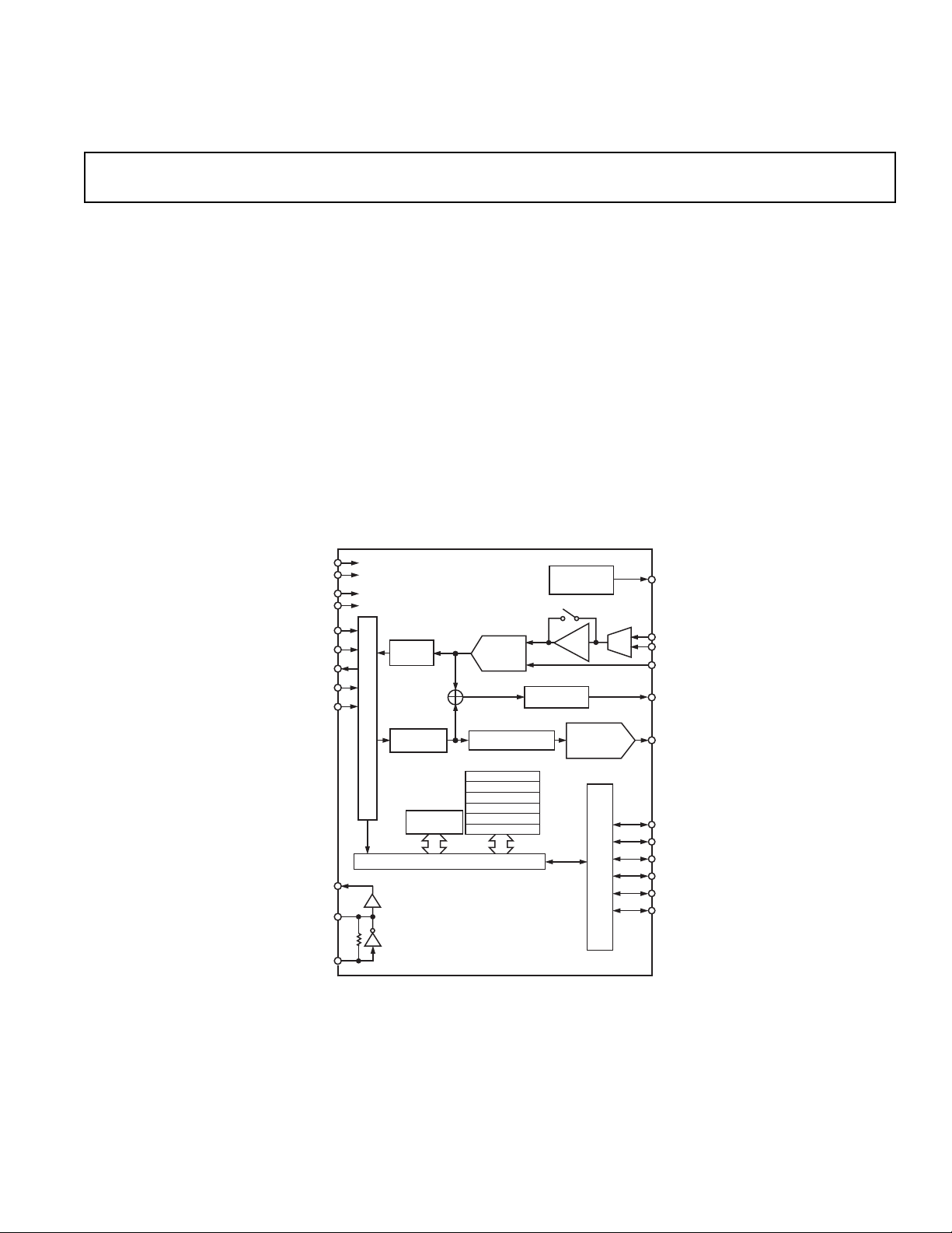
FUNCTIONAL BLOCK DIAGRAM
AVDD
AGND
DVDD
DGND
BIT_CLK
SYNC
SDATA_IN
SDATA_OUT
RESET
AC'97/DSP SERIAL PORT
ADC
FILTER
DAC
FILTER
AD1803
Digital Codec Engine with Variable Sample
Rate Conversion
Digital Monitor Speaker Output
24-Lead TSSOP Package
0.6 m CMOS Technology
Operation from 3.3 V or 5 V Supply
Advanced Power Management
APPLICATIONS
Modems (PC and Embedded)
Voice and Telephony
Fax Machines, Answering Machines, Speakerphones
PBX Systems
Smart Appliances
REFERENCE DESIGN
Available
⌺-⌬ ADC
PWM BLOCK
⌺-⌬ MODULATOR
VOLTAGE
REFERENCE
+20dB
DAC FILTER
+ GAIN
/ATTEN
MUX
VREF
G[1]/MIC
Rx
FILT
G[4]/MOUT
Tx
ADDRESS
REGISTER
REGISTER CONTROL LOGIC
CLK_OUT
XTALO
XTALI
REV. 0
Information furnished by Analog Devices is believed to be accurate and
reliable. However, no responsibility is assumed by Analog Devices for its
use, nor for any infringements of patents or other rights of third parties that
may result from its use. No license is granted by implication or otherwise
under any patent or patent rights of Analog Devices.
CONTROL
REGISTERS
G[0]
G[2]
G[3]/WAKE
G[5]
G[6]
GENERAL-PURPOSE I/O
One Technology Way, P.O. Box 9106, Norwood, MA 02062-9106, U.S.A.
Tel: 781/329-4700 www.analog.com
Fax: 781/326-8703 © Analog Devices, Inc., 2001
G[7]
Page 2

AD1803–SPECIFICATIONS
STANDARD TEST CONDITIONS UNLESS OTHERWISE NOTED
Temperature 25°C
Digital Supply 3.3 V/5 V
Analog Supply 3.3 V/5 V
Sample Rate (f
) 8 kHz
S
Input Signal 1008 Hz
Analog Output Pass Band 20 Hz to 4 kHz
ADC FFT Size 512
DAC FFT Size 4096
V
IH
V
IL
V
OH
V
OL
I
OH
I
OL
ADC RECEIVE PATH
2.1 V
1.2 V
2.9 V
0.3 V
–2.0 mA
+2.0 mA
Full-Scale Input Voltage (RMS Values Assume Sine Wave Input, PGA Gain = 0 dB,
Offset Error = 0% of FS) 1.56 V rms
AD1803 Rx Input (0 dBm) 2.1 2.2 2.3 V p-p
Resistance—Rx Input*
with 0 dB Gain 110 kΩ
with +20 dB Gain 10 kΩ
Capacitance—Rx Input* 15 pF
Rx Programmable Gain
Gain Step Size (0 dB to 42.5 dB, All Steps Tested) 1.0 1.5 2.0 dB
Input Gain Span (Note: The ADC Gain is achieved using a 0 dB to 22.5 dB Variable Gain 41.5 42.5 43.5 dB
Stage and a 20 dB Fixed Gain Stage. The 22.5 dB to 42.5 dB Gain Steps are achieved by
enabling the 20 dB Gain Stage.)
Analog-to-Digital Converter
Dynamic Range (–60 dB Input, THD+N Referenced to Full-Scale, PGA Gain = 0 dB) 85 90 dB
Dynamic Range (–60 dB Input, THD+N Referenced to Full-Scale, PGA Gain = 6 dB)* 90 dB
Dynamic Range (–60 dB Input, THD+N Referenced to Full-Scale, PGA Gain = +12 dB)* 90 dB
THD+N (–1 dB Input Referenced to Full-Scale) –90 –85 dB
Signal-to-Intermodulation Distortion (CCIF Method)* 80 dB
Offset Error (0 V Analog Input, PGA Gain = 0 dB) 1 5 % of FS
*Guaranteed, not tested.
Specifications subject to change without notice.
DAC Output Test Conditions
0 dB Attenuation Relative to Full-Scale
Input 0 dB
Mute Off
10 kΩ Output Load
ADC Input Test Conditions
Autocalibrated
0 dB PGA Gain
Mute Off
Input –1.0 dB Relative to Full-Scale
Min Typ Max Unit
DAC TRANSMIT PATH
Min Typ Max Unit
Digital-to-Analog Converter
Dynamic Range (–60 dB Input, THD+N Referenced to Full-Scale, Output Gain = 0 dB) 85 dB
THD+N (–1 dB Input Referenced to Full-Scale) –75 dB
Signal-to-Intermodulation Distortion (CCIF Method)* 80 dB
Total Out-of-Band Energy (Measured from 0.555 × f
to 100 kHz)* –40 dB
S
DC Offset 100 mV
Programmable Gain/Attenuator
Step Size (+12 dB to –34.5 dB, All Steps Tested) 1.0 1.5 2.0 dB
Output Attenuation Span 45.5 46.5 48 dB
Full-Scale Output Voltage
AD1803 Tx Output (0 dBm) 2.1 2.2 2.3 V p-p
Pin Capacitance—AD1803 Tx 15 pF
Load Capacitance—AD1803 Tx 100 pF
*Guaranteed, not tested.
Specifications subject to change without notice.
–2–
REV. 0
Page 3

AD1803
MONITOR OUTPUT
Min Typ Max Unit
Digital-to-Analog Converter
Dynamic Range (–60 dB Input, THD+N Referenced to Full-Scale, A-Weighted)* 50 dB
THD+N (Referenced to Full-Scale)* 0.316 1 %
–50 –40 dB
Programmable Gain/Attenuator
Step Size (–18 dB to +45 dB)* 2.4 3.0 3.6 dB
Output Attenuation Span* 63 dB
NOTES
*Guaranteed, not tested.
Specifications subject to change without notice.
The table above assumes the G[4]/MOUT pin is loaded with a 1 kΩ resistor in series with a parallel 4.7 kΩ resistor and 100 nF
capacitor combination tied to digital ground. This filter, with the output taken from the middle node, has a 1500 Hz corner to filter
out high-frequency Σ-∆ noise, and generates an approximate 1 V p-p output when using a 5 V digital supply with the monitor output
configured as first order (Bits MDM[1:0] set to 10 in Register 0 × 60 Bank 2) if the filter output load is greater than or equal
to 20 kΩ.
DIGITAL DECIMATION AND INTERPOLATION FILTERS
1
Min Typ Max Unit
Pass-Band Edge (–0.22 dB Point) 0.445 × f
Pass-Band (–3.0 dB Point) 0.490 × f
Hz
S
Hz
S
Pass-Band Ripple 0.0 –0.2 dB
Transition Band 0.445 × f
Stop-Band Edge
2
0.555 × f
S
S
0.555 × fSHz
Hz
Stop-Band Rejection (Plus 3 dB Roll-Off) 78.0 dB
Group Delay 21/f
S
s
Group Delay Variation Over Pass Band
0 kHz to 4 kHz 0.45 µs
0 kHz to 8 kHz 1.30 µs
Sample Rate 6.4 16 kHz
NOTES
1
Guaranteed, not tested.
2
The stop band repeats itself at multiples of 64 × fS, where fS is the sampling frequency. Thus the digital filter will attenuate to –78.0 dB or better across the frequency
spectrum except for a range ± 0.555 × fS wide at multiples of 64 × fS.
Specifications subject to change without notice.
TYPICAL SUPPLY CURRENT (For Most Common Modes of Operation)
Resource 3.3 V 5.0 V Register Writes To Enter Mode Assumption
GPIO Weak Pull-Up Current per Pin ~100 ~140 µA Default Settings After Power-On RESET
While RESET Is Asserted:
XTAL Off (All Down) <30.0 <40.0 µA Default Settings After Power-On RESET a
XTALI Enabled: Nominal Power 1.4 2.4 mA 5C:R34P4 = 1
XTALI Enabled: Low Power 1.0 1.7 5C:R34P4 = 1, 64b1:XTLP = 1
and CLKOUT Pin Running 1.6 3.2 and 5C:CLKEA = 1 b
While RESET Is Deasserted and Analog and Digital Codec in Full Power Mode
SPORT and CLKOUT Active 2.6 6.4 Default Settings After Power-On RESET b, c
and XTAL in Low Power Mode 2.2 5.7 and 64b1:XTLP = 1 b, c
and CLKOUT Inactive (Low) 1.7 4.3 and 5C:CLKED = 0 c
and VREF Powered Up 1.9 4.5 and 3E:VPDN = 0 c
and ADC Enabled 7.3 12.4 and 3E:APDN = 0 c
or
and DAC Enabled 8.2 13.7 and 3E:DPDN = 0 c, f
or
and ADC + DAC Enabled 9.2 14.7 and 3E:APDN = DPDN = 0 c, f
or
and ADC, DAC, + MON Enabled 9.3 14.9 and 3E:APDN = DPDN = 0, 5E : GPMON = 1 c, d, f
or
and ADC, DAC, + MON Enabled 10.2 16.3 and 3E:APDN = DPDN = 0, 5E : GPMON = 1 c, e, f
REV. 0
–3–
Page 4

AD1803
ASSUMPTIONS
a Assumes all inputs are static (not switching) and all output loads are capacitive (nonresistive).
b Excludes current drawn by CLKOUT pin board loading.
c Assumes the serial interface is configured in AC’97 primary mode with 20 pF loads on pins SDATA_IN and BIT_CLK. Typical current will be approximately
0.8 mA less if the serial interface is configured in DSP mode with 20 pF loads on pins SYNC, BIT_CLK, and SDATA_IN (due to a lower BIT_CLK frequency).
d Assumes a 20 pF load on Pin G[4]/MOUT.
e Assumes the G[4]/MOUT pin is loaded with a 1 kΩ resistor in series with a parallel 4.7 kΩ resistor and 100 nF capacitor combination tied to digital ground. This
filter, with the output taken from the middle node, has a 1500 Hz corner to filter out high-frequency Σ-∆ noise, and generates an approximate 1 V p-p output when
using a 5 V digital supply with the Monitor output configured as first order (Bits MDM[1:0] set to 10 in Register 0 × 60 Bank 2) if the filter output load is greater
than or equal to 20 kΩ.
f Assumes no DAC load. 0.6 mA should be added if a 600 Ω load is used.
g All currents in mA unless otherwise noted.
Specifications subject to change without notice.
STATIC DIGITAL SPECIFICATIONS
Min Typ Max Unit
High Level Input Voltage (V
Low Level Input Voltage (V
High Level Output Voltage (V
Low Level Output Voltage (V
Input Leakage Current –10 +10 µA
Output Leakage Current –10 +10 µA
Specifications subject to change without notice.
POWER SUPPLY
Power Supply Range—Analog (3.3 V/5 V) AVDD 3.0/4.75 3.6/5.25 V
Power Supply Range—Digital (3.3 V/5 V) DVDD 3.0/4.75 3.6/5.25 V
Analog and Digital Supply Current—5 V *
Analog and Digital Supply Current—3.3 V *
Power Supply Rejection (100 mV p-p Signal @ 1 kHz) 40 dB
(At Both Analog and Digital Supply Pins, Both ADCs and DACs)
NOTES
*Refer to table on typical supply current.
Specifications subject to change without notice.
): Digital Inputs 0.65 × DVDD V
IH
) 0.35 × DVDD V
IL
), IOH = –0.5 mA 0.9 × DVDD V
OH
), IOL = +0.5 mA 0.1 × DVDD V
OL
Min Typ Max Unit
CLOCK SPECIFICATIONS
Min Typ Max Unit
Input Clock Frequency 12.288 24.576 32.768 MHz
Recommended Clock Duty Cycle 45 50 55 %
Specifications subject to change without notice.
–4–
REV. 0
Page 5

AD1803
TIMING PARAMETERS (Guaranteed Over Operating Temperature Range and Supply Power)
Parameter Symbol Min Typ Max Unit
Serial Port—AC’97 Mode
RESET Active Low Pulsewidth t
RESET Inactive to BIT_CLK Start-Up Delay t
SYNC Active High Pulsewidth (Warm RESET)t
SYNC Inactive to BIT_CLK Start-Up Delay (Warm RESET)t
RST_LOW
RST2CLK
SYNC_HIGH
SYNC2CLK
BIT_CLK Frequency 12.288 MHz
BIT_CLK Period t
CLK_PERIOD
BIT_CLK Output Jitter* 750 ps
BIT_CLK High Pulsewidth t
BIT_CLK Low Pulsewidth t
CLK_HIGH
CLK_LOW
SYNC Frequency 48.0 kHz
SYNC Period t
Setup to Falling Edge of BIT_CLK t
Hold from Falling Edge of BIT_CLK t
Propagation Delay t
BIT_CLK Rise Time t
BIT_CLK Fall Time t
SYNC Rise Time t
SYNC Fall Time t
SDATA_IN Rise Time t
SDATA_IN Fall Time t
SDATA_OUT Rise Time t
SDATA_OUT Fall Time t
End of Slot 2 to BIT_CLK, SDATA_IN Low (MLNK Set) t
Setup to Trailing Edge of RESET t
SYNC_PERIOD
SETUP
HOLD
CO
RISECLK
FALLCLK
RISESYNC
FALLSYNC
RISEDIN
FALLDIN
RISEDOUT
FALLOUT
S2_PDOWN
SETUP2RST
(Applies to SYNC, SDATA_OUT)
Rising Edge of RESET to HI-Z Delay (ATE Test Mode) t
OFF
1.0 µs
162.8 ns
1.3 µs
162.8 ns
81.4 ns
36.62 40.69 44.76 ns
36.62 40.69 44.76 ns
20.8 µs
10.0 ns
10.0 ns
15 ns
246ns
246ns
246ns
246ns
246ns
246ns
246ns
246ns
2 1000 ns
15 ns
25 ns
Parameter Symbol Min Typ Max Unit
Serial Port—DSP Mode
RESET Active Low Pulsewidth t
RESET Inactive to BIT_CLK Start-Up Delay t
RST_LOW
RST2CLK
1.0 µs
162.8 ns
BIT_CLK Frequency 4.096 MHz
BIT_CLK Period t
CLK_PERIOD
244.14 ns
BIT_CLK Output Jitter* 750 ps
SYNC Frequency 8 kHz
SYNC Period t
Setup to Falling Edge of BIT_CLK t
Hold from Falling Edge of BIT_CLK t
Propagation Delay t
BIT_CLK Rise Time t
BIT_CLK Fall Time t
SYNC Rise Time t
SYNC Fall Time t
SDATA_IN Rise Time t
SDATA_IN Fall Time t
SDATA_OUT Rise Time t
SDATA_OUT Fall Time t
Setup to Trailing Edge of RESET t
SYNC_PERIOD
SETUP
HOLD
CO
RISECLK
FALLCLK
RISESYNC
FALLSYNC
RISEDIN
FALLDIN
RISEDOUT
FALLDOUT
SETUP2RST
10.0 ns
10.0 ns
246ns
246ns
246ns
246ns
246ns
246ns
246ns
246ns
15 ns
125 µs
15 ns
(Applies to SYNC, SDATA_OUT)
Rising Edge of RESET to HI-Z Delay (ATE Test Mode) t
NOTES
*Output jitter is directly dependent on crystal input jitter.
Specifications subject to change without notice.
OFF
25 ns
REV. 0
–5–
Page 6
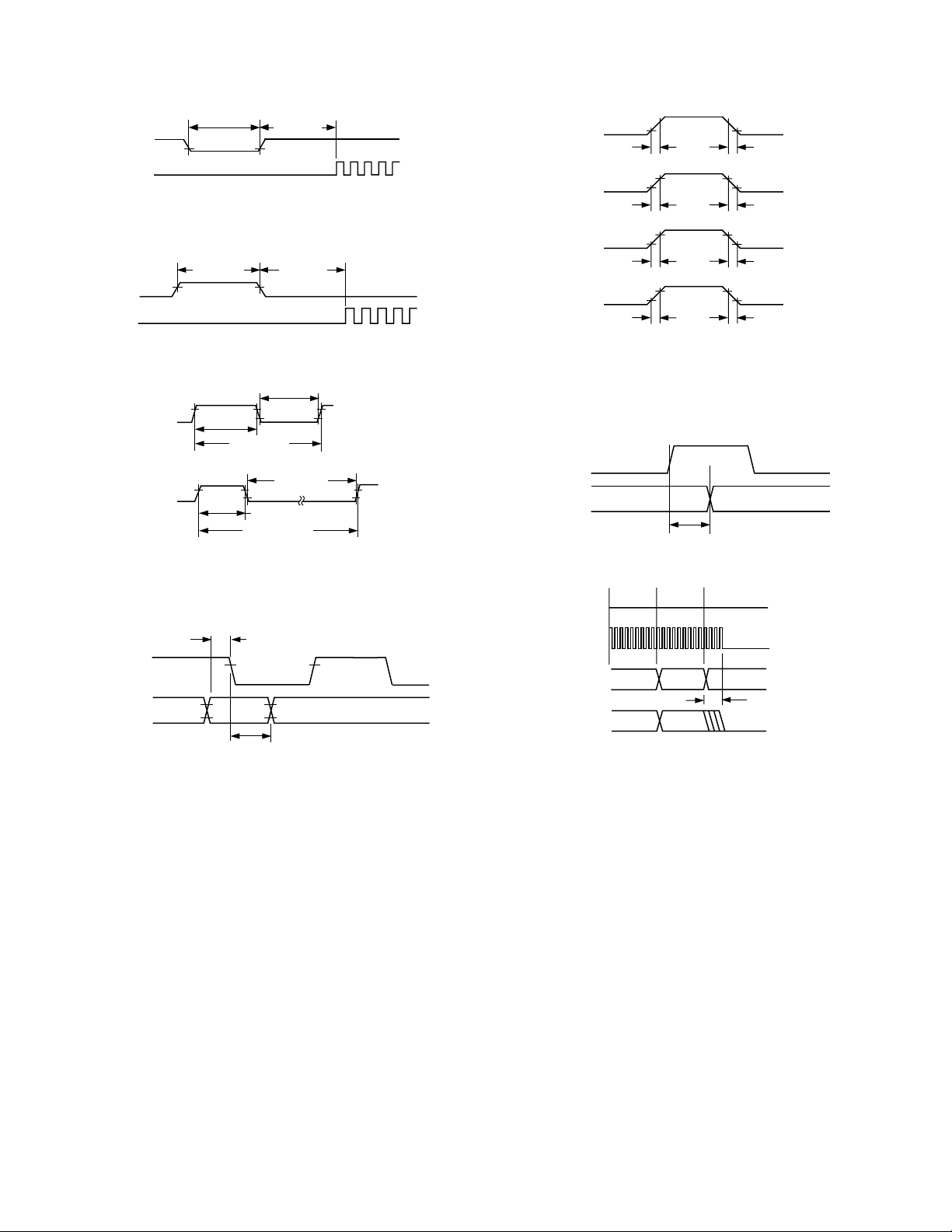
AD1803
RESET
BIT_CLK
SYNC
BIT_CLK
t
RST_LOW
Figure 1. Cold
t
SYNC_HIGH
t
RST2CLK
RESET
t
SYNC2CLK
BIT_CLK
SYNC
SDATA_IN
SDATA_OUT
t
RISECLK
t
RISESYNC
t
RISEDIN
t
RISEDOUT
t
FALLCLK
t
FALLSYNC
t
FALLDIN
t
FALLDOUT
BIT_CLK
SYNC
SDATA_OUT
Figure 2. Warm
BIT_CLK
SYNC
t
CLK_HIGH
t
CLK_PERIOD
RESET
t
CLK_LOW
t
SYNC_LOW
t
SYNC_HIGH
t
SYNC_PERIOD
Figure 3. Clock Timing
t
SETUP
t
HOLD
Figure 4. Data Setup and Hold
Figure 5. Signal Rise and Fall Time
BIT_CLK
SDATA_IN
t
CO
Figure 6. Propagation Delay
WRITE
SLOT 2
DATA
MLNK
DON’T
CARE
t
S2_PDOWN
SYNC
BIT_CLK
SDATA_OUT
SDATA_IN
SLOT 1
TO 0x56
NOTE: BIT_CLK NOT TO SCALE
Figure 7. AC Link Low Power Mode Timing
–6–
REV. 0
Page 7
AD1803
ABSOLUTE MAXIMUM RATINGS*
Min Max Unit
Power Supplies
Digital (DVDD) –0.3 +6.0 V
Analog (AVDD) –0.3 +6.0 V
Input Current (Except Supply Pins) ± 10.0 mA
Analog Input Voltage (Signal Pins) –0.3 AVDD
+ 0.3 V
Digital Input Voltage (Signal Pins) –0.3 DVDD + 0.3 V
Ambient Temperature (Operating) 0 70 °C
Storage Temperature –65 +150 °C
*Stresses greater than those listed under Absolute Maximum Ratings may cause
permanent damage to the device. This is a stress rating only; functional operation
of the device at these or any other conditions above those indicated in the
operational section of this specification is not implied. Exposure to absolute
maximum rating conditions for extended periods may affect device reliability.
ENVIRONMENTAL CONDITIONS
Ambient Temperature Rating
= T
T
AMB
= Case Temperature in °C
T
CASE
P
= Power Dissipation in W
D
= Thermal Resistance (Case-to-Ambient)
θ
CA
= Thermal Resistance (Junction-to-Ambient)
θ
JA
θ
= Thermal Resistance (Junction-to-Case)
JC
—(PD × θCA)
CASE
PACKAGE CHARACTERISTICS
Package
JA
TSSOP 83.8°C/W 15.6°C/W 68.2°C/W
ORDERING GUIDE
Model Temperature Range Package Description Package Option
AD1803JRU 0°C to 70°C 24-Lead Thin Shrink Small Outline Package RU-24
CAUTION
ESD (electrostatic discharge) sensitive device. Electrostatic charges as high as 4000 V readily
accumulate on the human body and test equipment and can discharge without detection.
Although the AD1803 features proprietary ESD protection circuitry, permanent damage may
occur on devices subjected to high-energy electrostatic discharges. Therefore, proper ESD
precautions are recommended to avoid performance degradation or loss of functionality.
JC
WARNING!
CA
ESD SENSITIVE DEVICE
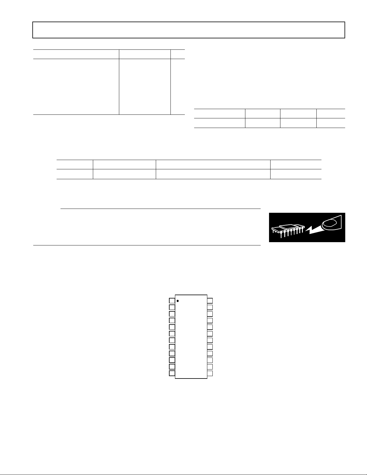
PIN CONFIGURATION
24-Lead TSSOP
(RU-24)
CLK_OUT G[5]
BIT_CLK AGND
SDATA_IN V
SDATA_OUT FILT
G[4]/MOUT G[0]
G[3]/WAKE G[2]
1
2
DGND
3
DVDD G[7]
4
XTALO AVDD
5
XTALI Tx
SYNC Rx
RESET
6
7
8
9
10
11
12
AD1803
TOP VIEW
(Not to Scale)
24
23
22
21
20
19
18
17
16
15
14
13
G[6]
REF
G[1]/MIC
REV. 0
–7–
Page 8

AD1803
PIN FUNCTION DESCRIPTIONS
Analog Signals
Pin Name TSSOP I/O Description
DVDD 3 I Digital Supply. Range: 5.0 V ± 10% or 3.3 V ± 10% (independent of AVDD).
DGND 2 I Digital Ground. Must be at same potential as AGND.
AVDD 21 I Analog Supply. Range: 5.5 V through 3.0 V (independent of DVDD).
AGND 19 I Analog Ground. Must be at same potential as DGND.
Clock Signals
Pin Name TSSOP I/O Description
XTALI 5 I Crystal or Clock Input (12.288, 24.576, or 32.768 MHz). This clock input is necessary
only if the AD1803 is configured in either AC’97 primary or DSP mode, or if a wake
interrupt from an event is required (in any mode). This pin must be tied to DVDD or DGND
(not floated) when clock input is not necessary. If a crystal is used, it must be parallel resonant first harmonic, and tied between this pin and the XTALO pin with load
capacitance specified by the crystal supplier. See Bits XTAL[1:0] in Register 0x5C for
further details.
XTALO 4 O Crystal Output. This pin should be floated when a crystal is not used.
CLK_OUT 1 O Buffered version of clock present on the XTALI pin, unless disabled. See Bits CLKED
and CLKEA in Register 0x5C for further details.
Serial Interface Signals (See Pins G[3:2] for Serial Interface Mode Selection)
Pin Name TSSOP I/O Description
RESET 10 I Active Low Power-Down. Level of power-down is determined by bits in Register 0x5C.
This pin must be asserted (driven LOW) as power is first applied until the supply is
stable. Contrary to the name of this pin, determined by Intel’s AC’97 specification, the
AD1803 is RESET exclusively by an internal power-on-RESET circuit.
BIT_CLK 6 I/O Serial Data Clock: Output if the AD1803 configured in AC’97 Primary or DSP mode,
Input if the AD1803 is configured in any AC’97 secondary mode.
SYNC 9 I/O Serial Data Frame Sync: Output if the AD1803 is configured in DSP mode, Input if the
AD1803 is configured in any AC’97 mode.
SDATA_IN 7 O Serial Data Output from AD1803.
SDATA_OUT 8 I Serial Data Input to AD1803.
General-Purpose I/O and Barrier Interface Signals
Pin Name TSSOP I/O Description
G[0] 14 I/O General-Purpose I/O.
G[1]/ 15 I General-Purpose I/O.
MIC I Or Analog MIC Input. See Bit GPMIC in Register 0x5E.
G[2] 13 I/O General-Purpose I/O. Also used to select Serial Interface mode (see below).
G[3]/ 12 I/O General-Purpose I/O.
WAKE O Or Wake Interrupt Output. See Bit GPWAK in Register 0x5E. Also used to select Serial
Interface mode (see below). When serving as WAKE, this pin will be driven high if
selected GPIO pins receive selected logic levels (see Registers 0x52 and 0x4E).
G[4]/ 11 I/O General-Purpose I/O.
MOUT O Or Monitor Output. See Bit GPMON in Register 0x5E.
G[5] 24 I/O General-Purpose I/O.
G[6] 23 I/O General-Purpose I/O.
G[7] 22 I/O General-Purpose I/O.
–8–
REV. 0
Page 9

AD1803
NOTES
1. See Registers 0x4C through 0x54 and Bank 1 Register 0x60 for G[7:0] (General Purpose I/O) pin control.
2. By default all G[7:0] pins serve as inputs with weak (~30 kΩ equivalent) internal pull-up devices enabled.
3. Input voltage on Pins G[7:2,0] must not exceed DVDD by more than 0.3 V.
4. Input voltage on Pin G[1] must not exceed AVDD by more than 0.3 V.
5. The states of pins G[3:2] are sampled when RESET is deasserted (driven from LOW to HIGH) for the first time after power is applied to select AD1803 serial
interface mode. Once sampled, serial interface mode can be changed only by removing power from the AD1803.
G[3]/WAKE G[2] Serial Interface Mode
HIGH HIGH AC’97 Mode—Primary Device (ID: 00)
HIGH LOW AC’97 Mode—Secondary Device (ID: 01)
LOW HIGH AC’97 Mode—Secondary Device (ID: 10)
LOW LOW DSP Mode
Analog Signals
Pin Name TSSOP I/O Description
Rx 16 I Receive (ADC) Input.
Tx 20 O Transmit (DAC) Output.
FILT 17 I ADC Filter Bypass: Requires 1 µF Capacitor to AGND.
V
REF
18 I Voltage Reference: Requires 1 µF Capacitor to AGND.
PRODUCT OVERVIEW
The AD1803 is a low power 16-bit codec for modem, voice,
and telephony applications. It can also be used as a cellular
telephone interface.
The AD1803 is an Intel AC’97 Rev 2.1-compliant modem
codec (refer to Intel’s AC’97 specifications at www.intel.com)
with selectable AC’97 or a DSP-style serial interface.
The AD1803 codec uses high-performance ⌺-⌬ ADC and DACs
with programmable gain/attenuation. It has a digital ⌺-⌬ monitor
output with selectable mix from ADC and DAC channels for
call progress monitoring.
The AD1803 supports advanced power management with
several power-saving modes. The codec supports seven general
purpose I/O pins and a wake interrupt signaling mechanism on
GPIO events.
SERIAL INTERFACE MODE SELECTION
When power is first applied to the AD1803, RESET must be
asserted (RESET pin driven LOW), and kept asserted until the
power has stabilized. While RESET is asserted, the AD1803’s
serial interface mode is chosen by the state of Pins 12 and 13:
Pin 12 Pin 13 Mode Chosen
HIGH HIGH AC’97 Mode—Primary Device (ID: 00)
HIGH LOW AC’97 Mode—Secondary Device (ID: 01)
LOW HIGH AC’97 Mode—Secondary Device (ID: 10)
LOW LOW DSP Mode
Note that Pins 12 and 13 have weak pull-up devices internal to
the AD1803 which are enabled by default. Therefore, if these
pins are floated, AC’97 primary mode will be chosen. When
RESET is deasserted (RESET pin driven HIGH) for the first
time after power is applied, the states of Pins 12 and 13 are
latched locking in serial interface mode. Subsequent changes of
logic level presented on Pins 12 and 13 will have no effect on
serial port mode until power is removed from the AD1803.
After this first deassertion of RESET, Pins 12 and 13 will take
on new roles and serve as general purpose I/O control pins. The
AD1803 does not need an active clock source for proper operation during this mode selection.
SERIAL INTERFACE BEHAVIOR AND PROTOCOL WHEN
IN AC’97 MODE
The AD1803 serial interface is compatible with the Intel’s
“Audio Codec ’97” Revision 2.1 specification as either a primary or secondary modem/handset codec device. Consult this
specification for complete behavioral details. By default the
AD1803 will use Slot 5 to send and receive sample data,
but this may be changed to Slot 10 or 11. See Bits SPCHN,
SPGBP, SPDSS, SPISO, and SPDL[1:0] in Register 0x5E for
additional AC’97 mode configuration enhancements.
AC’97 Interface Modes
Primary Mode
Entered if GPIO[3] pin is HIGH and GPIO[2] pin is HIGH
when RESET pin is deasserted first time:
AD1803 is Timing Master: Drives BIT_CLK @ 12.288 MHz
AD1803 accepts the 48 kHz SYNC Timing Signal
AD1803 requires a crystal or clock on XTALI (see Bits
XTALI[1:0] in Register 0x5C for frequency).
Secondary Modes
Entered if GPIO[3] pin is HIGH and GPIO[2] pin is LOW
when RESET pin is deasserted first time or if GPIO[3] pin is
LOW and GPIO[2] pin is HIGH when RESET pin is deasserted
first time:
AD1803 is Timing Slave: Accepts BIT_CLK @ 12.288 MHz
AD1803 accepts the 48 kHz SYNC Timing Signal
AD1803 does not require a crystal or clock on XTALI (see Bits
XTALI[1:0] in Register 0x5C for frequency) unless wake from
an event during RESET is desired.
REV. 0
–9–
Page 10

AD1803
SLOT #
SYNC
SDATA_OUT
SDATA_IN
TAG CMD
(OUTPUT FROM CONTROLLER/DSP – INPUT TO AD1803)
TAG STATUS
(INPUT TO CONTROLLER/DSP – OUTPUT FROM AD1803)
10 23456789101112
CMD
ADDR
STATUS
ADDR
PCMLPCMRLINE1
DATA
PCMLPCMRLINE1
DATA
DAC
ADC
Figure 8. AC’97 Interface Timing
SERIAL INTERFACE BEHAVIOR AND PROTOCOL WHEN IN DSP MODE
In DSP mode, the AD1803 requires a clock on XTALI to do
anything useful. This clock can be created by placing a crystal
between pins XTALI and XTALO with appropriate trim
capacitors. Alternatively, a clock can be driven directly onto the
XTALI pin from an external source, in which case XTALO
must be floated. When the AD1803 serial interface is configured
in DSP mode, the clock presented on the XTALI pin is assumed
to be 24.576 MHz. However, a 12.288 MHz or 32.768 MHz
clock could be used instead, providing:
1. The AD1803 is informed via a register write what the true
clock frequency is before the codec is enabled; and
2. It is acceptable to have the serial port Bit clock and frame
sync run at rates different from the start-up nominal until the
AD1803 is informed of the true XTALI clock frequency.
Within 1 ms after RESET is deasserted and the AD1803 receives a
clock on XTALI, the AD1803 will begin driving a 4.096 MHz
Bit clock onto the BIT_CLK pin (assuming a 24.576 MHz
XTALI clock). Approximately 100 µs later, the AD1803 will
begin driving an 8 kHz frame sync onto the SYNC pin (again
assuming a 24.576 MHz XTALI clock). If the AD1803 receives an
XTALI clock that is higher/lower than the expected 24.576 MHz
default, these frequencies will be scaled up/down (lineally) until
the AD1803 is informed of the actual XTALI clock frequency by a
write to Bits XTAL[1:0] in Register 0x5C. See Bits XTAL[1:0]
for further details including allowed alternate XTALI frequencies.
Each serial interface frame consists of a single 16-Bit word sent
into the AD1803 on the SDATA_OUT pin, and a single 16-Bit
word sent out of the AD1803 on the SDATA_IN pin. These
words are simultaneously transferred during the first 16 clocks
of the BIT_CLK pin after the start of a frame. The start of a
frame is marked by a one BIT_CLK long HIGH pulse of the
SYNC pin one BIT_CLK period before the first bit in the frame.
Data is transmitted MSB first. Logic levels on all pins (SYNC,
SDATA_IN, and SDATA_OUT) are updated on BIT_CLK
rising edges, and should be sampled on BIT_CLK falling edges.
By default all frames are designated as data frames for delivery of two’s complement DAC and ADC samples to and from
the AD1803’s codec. To deliver control information into the
AD1803, the LSB of the word into the AD1803 has been stolen
from what might otherwise have been DAC data to serve as a
control frame request bit. While the AD1803 provides 16-bit
ADC sample output, only 15-bit DAC sample input is
PCM
PCM
PCM
PCM
LINE2
CENTER
L SURR
R SURR
MIC
RSRVD RSRVD RSRVD LINE2
ADC
LFE
DAC
ADC
HSET
DAC
HSETADI/O
I/O
CTRL
STATUS
possible because of this. If the LSB of the word into the
AD1803 is set to 0, no control frame is requested and the next
frame will be another data frame. If the LSB of the word into
the AD1803 is set to 1, a control frame is requested and the
next frame will be a control frame.
When a control frame is requested, an extra frame is inserted
between data frames avoiding an interruption of codec sample
data flow. The 16-bit control word into the AD1803 consists of,
from MSB to LSB: a register read/write request bit (0 to request
a write, 1 to request a read); the six MSBs of a 7-bit register
address (where the LSB is removed to save space since it’s
always a 0); a byte select bit (0 to select the lower byte of the
16-bit control register addressed, 1 to select the upper byte of
the 16-bit control register addressed); and, finally, eight bits of
data that will be written into the addressed register if a write is
requested. Otherwise, these last eight bits will be ignored. While
it may seem peculiar to have a 7-bit register address with an
always 0 LSB consequently dropped when sent to the AD1803,
it should be noted that AD1803 register addresses are defined
by the AC’97 specification, whether configured in an AC’97 mode
or in DSP mode. While the AC’97 2.1 specification reserves odd
addresses for future feature expansion, there was not room in a
DSP mode control word for this unused bit. The 16-bit control
word out of the AD1803 consists of, from MSB to LSB, eight
unused bits that are always 0s, followed by eight bits of data
that reflect the contents of the register addressed within the
current frame if a read was requested. Otherwise they are all 0s.
When serial interface frames first commence after RESET is
deasserted, there will be 512 bits per frame (8 kHz frame rate/
4.096 MHz bit clock rate) where only the first 16 bits per frame
are typically utilized. Bits out of the AD1803 after the first 16
will typically all be set to 0, and bits into the AD1803 after the
first 16 are typically ignored. However, when a control frame
is requested via the control frame request bit in a data frame, the
control frame will be inserted between data frames, and placed
256 bits after the start of the data frame that requested the control
frame. This control frame will of course be marked by an
additional 1-bit clock long pulse HIGH of the SYNC pin. Note
that the spacing between data frames is always unaffected by
the insertion of a control frame.
Although at Startup the frame rate is 8 kHz and there are
exactly 512 bits from the start of one data frame to the next, this
will change as soon as the codec is enabled (note that the codec
is powered down by default after power is first applied to the
AD1803). Whenever the codec is enabled, the frame rate will be
–10–
REV. 0
Page 11

)
FRAME TYPES:
SYNC
BIT_CLK
DATA FRAME (16 BITS):
SDATA_OUT
AD1803
FREQUENCY: 8kHz WHEN CODEC DISABLED, AND EQUAL TO SAMPLE RATE WHEN CODEC ENABLED
FREQUENCY: 4.096MHz
T15 T14 T13 T12 T11 T10 T9 T8 T7 T6 T5 T4 T3 T2 T1 CR
INPUT TO AD1803 (15 TRANSMIT SAMPLE DATA BITS, PLUS CONTROL FRAME REQUEST BIT)
SDATA_IN
CONTROL FRAME
(16 BITS):
SDATA_OUT
SDATA_IN
FRAME ORDERING:
SYNC
SDATA_OUT
SDATA_IN
C15 C14 C13 C12 C11 C10 C9 C8 C7 C6 C5 C4 C3 C2 C1 C0
OUTPUT FROM AD1803 (16 CAPTURE SAMPLE DATA BITS)
RW A6 A5 A4 A3 A2 A1 B W7 W6 W5 W4 W3 W2 W1 W0
INPUT TO AD1803 (READ/WRITE, ADDRESS, AND BYTE SELECT, FOLLOWED BY EIGHT BITS OF
REGISTER WRITE DATA)
R7 R6 R5 R4 R3 R2 R1 R0
OUTPUT FROM AD1803 (EIGHT ZEROS, FOLLOWED BY EIGHT BITS OF REGISTER READ DATA ADDRESSED
BY THIS FRAME
Figure 9. Frame Types
FRAME INSERTED IF REQUESTED BY CR BIT
DATA FRAME CONTROL FRAME DATA FRAME
T15:1, CR IGNORED
C15:0 R7:0 C15:0
PERIOD EQUALS 1/8kHz WHEN CODEC IS DISABLED AND
PROGRAMMED SAMPLE PERIOD WHEN CODEC IS ENABLED
RW, A6:1,
B, W7:0
IGNORED T15:1, CR IGNORED
Figure 10. Frame Ordering
switched from 8 kHz to the programmed codec sample rate,
and whenever the codec is powered down again, the frame
rate will switch back to 8 kHz. With the bit clock always fixed
at 4.096 MHz, this gives rise to a first cause of variation in the
number of bits between starts of data frames. A second cause of
varying number of bits between starts of data frames is the
presence of a subtle jitter in the assertion of frame sync when
the codec is enabled. Although on average there will be an exact
match between the programmed sample rate and the frame rate,
the frame sync itself will vary up to 4% of a sample period from
the ideal assertion point in time.
When the serial interface is in DSP mode, it is possible to access
only the upper or lower 8-bit byte of a 16-bit control register at
REV. 0
–11–
a time. While this is sufficient for manipulating many of the
AD1803 features, some features require more than eight control
bits and span multiple 8-bit bytes and/or multiple 16-bit words.
To allow all bits of a feature to take effect simultaneously, writes
to certain control bytes of certain registers are actually held in
holding latches until a particular control byte of the feature is
written. Note that a read of a control register always returns the
contents of a holding latch (if present for that register), which
does not necessarily reflect the control setting currently being
used by the AD1803. The only feature in the AD1803 that
incorporates this complication is the codec sample rate, which
writes to the lower byte of Register 0x40 and does not take
effect until the upper byte of Register 0x40 is written.
Page 12

AD1803
REGISTER BANKS
Register addresses are based on Intel’s AC’97 specification.
However, since the AC’97 specification lacks sufficient vendordefined register space to control all extended features of the
AD1803, some control registers must be accessed indirectly using
register banks. See Bits BNK[1:0] in Register 0x5C for details.
REGISTER ACCESS RESTRICTIONS
Nearly all control registers may be read or written at any time.
However, below is a list of restrictions that must be followed to
ensure proper operation of the AD1803:
1. The clock frequency delivered to the AD1803 on XTALI
must be identified (via a write to Bits XTAL[1:0] in Register
0x5C) before the codec is enabled (via a write of 0 to Bits
DPDN or APDN in Register 0x3E).
2. During ADC calibration, codec sample rate (Register 0x40),
and ADC source and gain level must not be changed, and
digital impedance synthesis (see DISE bit in Register 0x5E)
must not be enabled. Calibration is initiated each time the
AD1803’s ADC is enabled (see Bit APDN in Register 0x3E)
and whenever a 1 is written to Bit ADCAL in Register 0x5C.
Completion of calibration may be determined by polling the
ADCAL bit.
GENERAL-PURPOSE I/O PIN OPERATION
Refer to Registers 0x4C through 0x54 and Bank 1 Register 0x60
for complete details. See Figure 12.
Table I. Voice Features
F
eature AD1803
Power Supply 3 V to 5 V
Maximum Sampling Frequency 16 kHz
Differential Handset Output No
Single-Ended Line Output Yes, 600 Ω Load
Output Full-Scale Range 2.2 V p-p
Output Attenuation Steps +12 dB to –34.5 dB
Input Line/MIC Mux Yes
Input Full-Scale Range 0.777 V rms
2.2 V p-p
Input 0 dB/20 dB Gain Block Yes
PGA, 0 dB–22.5 dB Range Yes
Single-Ended Input Yes
Differential Input No
Input Resistance 10 kΩ min Varies with Gain
(See Table II)
Table II. Input Resistance vs. Gain Setting
PGA Gain 20 dB PGA Gain R
IN
(dB) Gain Block (dB) (k⍀)
0.0 to 22.5 Disabled 0.0 to 22.5 100
0.0 to 22.5 Enabled 20.0 to 42.5 10
VOICE/HANDSET SUPPORT
In addition to modem applications, the AD1803 can be used for
Voice/Handset support.
GPIO[n] OUTPUT DATA
AC'97 MODES: FROM AC-LINK SLOT12
DSP MODE: FROM REG. 0ⴛ54
INTERRUPT
AC '97 MODE SLOT 12, OR
GPIO STATUS (REG. 0x54[n])
OTHER INTERRUPT SOURCES
WAKE ENABLE (REG. 0x52[n])
TRIGGERED BY "0" WRITE TO:
STATUS (REG. 0x54[n])
1
STICKY (REG. 0x50[n])
0
STICKY (REG. 0x50[n])
0 = NONSTICKY INPUT
1 = STICKY INPUT
CONFIG (REG. 0x4C[n])
0 = OUTPUT
1 = INPUT
POLARITY (REG. 0x4E[n])
0 = CMOS
1 = OPEN DRAINS
SRQ
GPIO[n] PIN
DVDD
WEAK MOS
POLARITY (REG. 0x4E[n])
0 = ACTIVE HIGH
1 = ACTIVE LOW
Figure 11. Conceptual Diagram of GPIO Pin Behavior
–12–
REV. 0
Page 13

AD1803
Table III. Register Summary
Direct Mapped Registers Indirect Mapped Registers
Address Register Name Address Register Name
0x3C Extended Modem ID
0x3E Extended AD1803 Status and Control
0x40 Line DAC/ADC Sample Rate Control
0x46 AD1803 DAC/ADC Level Control
0x4C GPIO Pin Configuration
0x4E GPIO Pin Polarity/Type
0x50 GPIO Pin Sticky
0x52 GPIO Pin Wake-Up Mask 0x60 In Bank 1 AD1803 GPIO Initial States
0x54 GPIO Pin Status
0x56 Misc. Modem AFE Status and Control 0x64 In Bank 1 AD1803 Clock Pad Control
0x5C AD1803 Configuration 1 0x60 In Bank 2 AD1803 Monitor Output Control
0x5E AD1803 Configuration 2
0x7A AD1803 Version ID
0x7C Vendor ID1
0x7E Vendor ID2
Table IV. Register Bit Mapping
Adr/Bnk Default D15 D14 D13 D12 D11 D10 D9 D8 D7 D6 D5 D4 D3 D2 D1 D0
0x3C ID1 ID0 0 0 0 0 0 0 0 000000LIN1
0x3E 0xFF00 Res Res Res Res DPDN APDN VPDN GPDN 0 0 0 0 DSTA ASTA VSTA GSTA
0x40 0x3E80 SRG1 SRG0 SR13 SR12 SR11 SR10 SR9 SR8 SR7 SR6 SR5 SR4 SR3 SR2 SR1 SR0
0x46 0x8080 DAM 0 0 DAL4 DAL3 DAL2 DAL1 DAL0 ADM 0 ADS ADG20 ADL3 ADL2 ADL1 ADL0
0x4C 0x00FF 0 0 0 0 0 0 0 0 GC7 GC6 GC5 GC4 GC3 GC2 GC1 GC0
0x4E 0x00FF 0 0 0 0 0 0 0 0 GP7 GP6 GP5 GP4 GP3 GP2 GP1 GP0
0x50 0x0000 0 0 0 0 0 0 0 0 GS7 GS6 GS5 GS4 GS3 GS2 GS1 GS0
0x52 0x0000 0 0 0 0 0 0 0 0 GW7 GW6 GW5 GW4 GW3 GW2 GW1 GW0
0x54 0x00FF 0 0 0 0 0 0 0 0 GI7 GI6 GI5 GI4 GI3 GI2 GI1 GI0
0x56 0x0000 0 0 0 MLNK 0 0 0 0 0 0000L1B2 L1B1 L1B0
0x5C 0x18C0 Res BNK1 BNK0 R34PM XTAL1 XTAL0 ACSEL ADCAL CLKED CLKEA Res Res Res Res Res Res
0x5E 0x0018 GPBAR GPWAK GPMON GPMIC SPCHN SPGBP SPDSS SPISO SPDL1 SPDL0 Res Res Res Res Res Res
0x60/1 0 0 0 0 0 0 0 0 GPIV7 GPIV6 GPIV5 GPIV4 GPIV3 GPIV2 GPIV1 GPIV0
0x64/1 0x0077 0 0 0 0 0 0 0 0 Res Res Res Res XTLP COS2 COS1 COS0
0x60/2 0x4000 MMD1 MMD0 MDM MDL4 MDL3 MDL2 MDL1 MDL0 Res Res MAM MAL4 MAL3 MAL2 MAL1 MAL0
0x7A 0x0002 0 0 0 0 0 0 0 0 VER7 VER6 VER5 VER4 VER3 VER2 VER1 VER0
0x7C 0x4144 0 1 0 0 0 0 0 1 0 1000100
0x7E 0x5380 0 1 0 1 0 0 1 1 1 0000000
Res = Reserved Bit. To ensure future compatibility, reserved bits should be set to “0” when written and ignored when read.
REV. 0
–13–
Page 14

AD1803
REGISTER DESCRIPTION
Extended Modem ID Register Address 0x3C
51D41D31D21D11D01D9D8D7D6D5D4D3D2D1D0D
1DI0DI 0000000000000 1NIL
A write to this register has no effect on the states of bits within this register, but does trigger Register 0x3E and Bank 2 Register 0x60
to be cleared to their default states, which powers down the AD1803’s codec resources.
ID[1:0] Interface Identification. These bits may be read to determine the AD1803’s serial interface mode of operation.
Serial interface mode is chosen by the states of Pins 13 and 12 when RESET is deasserted (RESET pin driven
from LOW to HIGH) for the first time after power is applied to the AD1803.
00 = AC-Link Primary (mode chosen if Pin 12 is HIGH and Pin 13 is HIGH on first deassertion of RESET).
01 = AC-Link Secondary (mode chosen if Pin 12 is HIGH and Pin 13 is LOW on first deassertion of RESET).
10 = AC-Link Secondary (mode chosen if Pin 12 is LOW and Pin 13 is HIGH on first deassertion of RESET).
11 = DSP-Link (mode chosen if Pin 12 is LOW and Pin 13 is LOW on first deassertion of RESET).
LIN1 Modem Line 1 Supported. For AC’97 compatibility, this bit returns a 1 when read to indicate that the AD1803
supports AC’97 modem line 1 features.
Extended AD1803 Status and Control Default = 0xFF00 Address 0x3E
51D41D31D21D11D01D9D8D7D6D5D4D3D2D1D0D
seRseRseRseRNDPDNDPANDPVNDPG 0000 ATSDATSAATSVATSG
Res = Reserved Bit. To ensure future compatibility, reserved bits should be set to “0” when written and ignored when read.
This register is forced to its default when: 1) Power is first applied to the AD1803; 2) The RESET pin is driven LOW; or 3) Register
0x3C is written with any value.
DPDN AD1803 DAC Power-Down. When this bit is set to 1 (default), all DAC resources within the AD1803 will be
powered down, and all DAC data sent to the AD1803 over the serial interface will be ignored. When this bit is set
to 0, the digital DAC resources within the AD1803 will be powered up, but the analog DAC resources within
the AD1803 will be powered up only if the AD1803’s voltage reference is powered up (Bit VPDN in this register set to 0), and the AD1803’s analog codec is selected as the partner to the AD1803’s digital codec (Bit ACSEL
in Register 0x5C set to 0).
0 = Enable AD1803 Digital DAC Resources, Conditionally Enable AD1803 Analog DAC Resources.
1 = Power-Down All AD1803 DAC Resources (default).
APDN AD1803 ADC Power-Down. When this bit is set to 1 (default), all ADC resources within the AD1803 will be
powered down, and all ADC data words sent out of the AD1803 over the serial interface will be midscale (zero)
(and tagged invalid if the serial interface is configured in an AC’97 mode). When this bit is set to 0, the digital
ADC resources within the AD1803 will be powered up, but the analog ADC resources within the AD1803 will be
powered up only if both the AD1803’s voltage reference is powered up (Bit VPDN in this register set to 0), and
the AD1803’s analog codec is selected as the partner to the AD1803’s digital codec (Bit ACSEL in Register 0x5C
set to 0). Each time the AD1803’s analog codec is powered up, an ADC DC offset calibration is automatically
initiated. This calibration requires approximately 104 sample periods (defined by Register 0x40), but cannot be
started until after the AD1803’s voltage reference is powered up (by setting Bit VPDN in this register to 0),
which itself requires about 48 ms. Bit VSTA in this register may be polled first to determine if the voltage reference
is powered up, and then Bit ADCAL in Register 0x5C may be polled to determine if calibration is completed.
During calibration, codec sample rate, ADC source, and ADC gain level must not be changed.
0 = Enable AD1803 Digital ADC Resources, Conditionally Enable AD1803 Analog ADC Resources.
1 = Power-Down All AD1803 ADC Resources (default).
VPDN AD1803 Voltage Reference Power-Down. Writes to this bit initiate codec voltage reference power-up and power-
down sequences. Bit VSTA in this register may be polled to monitor current voltage reference status. Until the
voltage reference is fully powered up, the AD1803’s analog ADC and DAC channels will ignore the setting of Bits
APDN and DPDN and remain powered down.
0 = Enable Voltage Reference.
1 = Power-Down Voltage Reference (default).
–14–
REV. 0
Page 15

AD1803
GPDN AD1803 GPIO Power-Down. The setting of this bit affects the behavior of the AD1803 only when it is configured
in an AC’97 mode (see Register 0x3C). This bit determines whether or not the logic levels received on the AD1803’s
GPIO (general purpose IO) pins are reflected on bits in Slot 12 of the AC’97 link, and whether or not the states of
bits in Slot 12 determine the logic levels to drive out of GPIO pins that are configured as outputs. See Bit SPGBP in
Register 0x5E for mapping. Contrary to the AC’97 specification, the setting of this bit does not actually control the
power-up/down state of GPIO pins. AD1803 GPIO pins are always powered up and always perform the functions they are assigned by the programming of Registers 0x4C through 0x54 and Register 0x5E.
0 = Slot 12 Output Bits Reflect Logic Levels Received on GPIO Pins.
Slot 12 Input Bits Determine Logic Levels to Drive out GPIO Pins Configured as Outputs.
1 = Slot 12 Output Bits All 0 (default).
Slot 12 Input Bits are Ignored.
DSTA AD1803 DAC Status. This bit exists solely for AC’97 compatibility. Its purpose is to provide a handshake for
DAC power-up/-down status changes initiated by writes to Bit DPDN in this register. However, since the AD1803
will respond to a write of Bit DPDN prior to it being possible to read this bit in a following serial interface frame,
it’s pointless to poll this status bit. Writes to this bit have no effect on AD1803 behavior.
ASTA AD1803 ADC Status. This bit exists solely for AC’97 compatibility. Its purpose is to provide a handshake for
ADC power-up/-down status changes initiated by writes to Bit APDN in this register. However, since the AD1803
will respond to a write of Bit APDN prior to it being possible to read this bit in a following serial interface frame,
it’s pointless to poll this status bit. Writes to this bit have no effect on AD1803 behavior.
VSTA AD1803 Voltage Reference Status. This bit may be polled to monitor the status of the AD1803’s codec voltage
reference. When read as a 0, the voltage reference is either powered down or in the process of powering up. When
read as a 1, the voltage reference is either powered up or in the process of powering down. Approximately 48 ms after
Bit VPDN in this register is set to a 0, this bit will transition from a 0 to a 1 indicating that the voltage reference is
fully powered up. Approximately 0.8 ms after VPDN is set to a 1, this bit will transition from a 1 to a 0 indicating
that the voltage reference is fully powered-down. If a clock is driven onto the AD1803’s XTALI pin (rather than
generated by a crystal placed between the XTALI and XTALO pins), and it is desired to stop this clock for additional
system power savings, this clock must not be stopped until after this bit falls to a 0. Writes to this bit have no effect
on AD1803 behavior.
GSTA AD1803 GPIO Status. This bit exists solely for AC’97 compatibility. Its purpose is to provide a handshake for
DAC power-up/-down status changes initiated by writes to Bit GPDN in this register. However, since the AD1803
will respond to a write of Bit GPDN prior to it being possible to read this bit in a following serial interface frame, it
is pointless to poll this status bit. Writes to this bit have no effect on AD1803 behavior.
Line DAC/ADC Sample Rate Control Default = 0x3E80 Address 0x40
51D41D31D21D11D01D9D8D7D6D5D4D3D2D1D0D
1GRS0GRS31RS21RS11RS01RS9RS8RS7RS6RS5RS4RS3RS2RS1RS0RS
This register is forced to its default only when power is first applied to the AD1803.
This register must not be written while an ADC calibration is in progress (see Bit APDN in Register 0x3E and Bit ADCAL in
Register 0x5C).
When the AD1803 serial interface is configured in DSP mode, writes to the lower byte of this register are temporarily placed in a
holding register and do not actually take effect until the upper byte is written. This ensures that the 16-bit sample rate takes effect
only as a whole. Reads of the lower byte of this register return the contents of this holding register which does not necessarily reflect
the current sample rate.
SRG[1:0] Sample Rate Granularity. Together with Bits P4MS[1:0] in Register 0x5C, these bits select the LSB weighting of
the Bits SR[13:0] (Sample Rate Select). These bits select a fundamental LSB weighting of either 1 Hz, 8/7 Hz, or
10/7 Hz for Bits SR[13:0], while Bits P4MS[1:0] may be used to put the codec in a low power mode in which case
these fundamental LSB weighings are cut in half.
00 = SR[13:0] LSB Weight Is 1 Hz If P4MS[1:0] != 10 (default), Or 1/2 Hertz If P4MS[1:0] = 10.
01 = SR[13:0] LSB Weight Is 8/7 Hz If P4MS[1:0] != 10, Or 4/7 Hz If P4MS[1:0] = 10.
10 = SR[13:0] LSB Weight Is 10/7 Hz If P4MS[1:0] != 10, Or 5/7 Hz If P4MS[1:0] = 10.
11 = Reserved.
REV. 0
–15–
Page 16

AD1803
SR[13:0] Sample Rate Select. Together with Bits SRG[1:0] (Sample Rate Granularity) and Bits P4MS[1:0] in Register
0x5C, these bits define the sample rate for both the ADC and DAC codec channels. Permitted settings of
SR[13:0] range from 6400 to 16000 when SRG[1:0] = 00, 5600 to 14000 when SRG[1:0] = 01, and 4480 to
11200 when SRG[1:0] = 10. Resultant sample rate, regardless of SRG[1:0] setting, always ranges from 6,400 Hz
to 16,000 Hz if the codec is not in low power mode (P4MS[1:0] 1 = 10), and ranges from 3,200 Hz to 8,000 Hz if
the codec is in low power mode (P4MS[1:0] = 10). The default sample rate is 16000 Hz.
AD1803 DAC/ADC Level Control Default = 0x8080 Address 0x46
51D41D31D21D11D01D9D8D7D6D5D4D3D2D1D0D
MAD004LAD3LAD2LAD1LAD0LADMDA0SDA02GDA3LDA2LDA1LDA0LDA
This register is forced to its default only when power is first applied to the AD1803.
The states of Bits ADS, ADG20, and ADL[3:0] in this register must not be changed while an ADC calibration is in progress if the
AD1803’s analog codec is in use (see Bit APDN in Register 0x3E and Bit ADCAL in Register 0x5C).
DAM DAC Mute.
0 = DAC Output Enabled.
1 = DAC Output Muted (Forced to Midscale) (default).
DAL[4:0] DAC Attenuation Level Select. Least significant bit represents –1.5 dB. This attenuation is valid when the
AD1803’s analog codec is used with the AD1803’s digital codec (Bit ACSEL in Register 0x5C = 0)
00000 = +12.0 dB Gain (default).
11111 = –34.5 dB Attenuation.
ADM ADC Mute.
0 = ADC Samples Passed.
1 = ADC Samples Substituted with Midscale (Zero) Data (default).
ADS AD1803 Analog ADC Input Select. The state of this bit has no effect on ADC behavior unless Bit ACSEL in
Register 0x5C is set to 0 (default). This selects the AD1803’s analog codec to partner the AD1803’s digital
codec. If this bit will be used to select the MIC input as the AD1803’s ADC input, Pin 15 must first be assigned
to serve as this MIC input rather than its default role as a GPIO (General Purpose IO) pin. This is done by
setting Bit GPMIC in Register 0x5E to 1.
0 = Pin 16 (Rx Input) Selected As AD1803 ADC Input Source (default).
1 = Pin 15 (MIC Input) Selected As AD1803 ADC Input Source (requires GPMIC in Register 0x5E set to 1).
ADG20 AD1803 Analog ADC 20 dB Gain Enable. The state of this bit has no effect on ADC behavior unless Bit ACSEL in
Register 0x5C is set to 0 (default). This selects the AD1803’s analog codec to partner the AD1803’s digital
codec. Total ADC gain will be the summation due to this bit and Bits ADL[3:0].
0 = 0 dB Gain (default).
1 = 20 dB Gain.
ADL[3:0] AD1803 ADC Gain Level Select. The state of these bits has no effect on ADC behavior unless Bit ACSEL in
Register 0x5C is set to 0 (default). This selects the AD1803’s analog codec to partner the AD1803’s digital codec.
Total ADC gain will be the summation due to these bits and Bits ADG20. Least significant bit represents 1.5 dB.
0000 = 0.0 dB Gain (default).
1111 = 22.5 dB Gain.
GPIO Pin Configuration Default = 0x00FF Address 0x4C
51D41D31D21D11D01D9D8D7D6D5D4D3D2D1D0D
0000000 0 7CG6CG5CG4CG3CG2CG1CG0CG
This register is forced to its default only when power is first applied to the AD1803.
GC[7:2,0] General Purpose IO Pin Configuration. These bits define the directionality of GPIO pins with corresponding numbers.
By default, all GPIO pins serve as inputs but with weak (~100 µA with a 3.3 V supply, ~140 µA with a 5.0 V sup-
ply) pull-up devices internal to the AD1803 enabled. See Register 0x4E to disable these weak pull-up devices.
Note that GPIO Pin 1 is always an input and cannot serve as an output. Also note that bits in this register will be
ignored if the GPIO pin they control has been assigned to serve an alternate special purpose (see bits in Register
0x5E). Care must be taken to insure that GPIO pin input voltages never exceed GPIO supply and ground voltages
by more than 0.3 V. GPIO Pin 1 is source by the analog supply (Pins AVDD and AGND). All other GPIO pins
are sourced by the digital supply (Pins DVDD and DGND).
0 = GPIO Pin Serves as an Output.
1 = GPIO Pin Serves as an Input (default).
–16–
REV. 0
Page 17

AD1803
GPIO Pin Polarity/Type Default = 0x00FF Address 0x4E
51D41D31D21D11D01D9D8D7D6D5D4D3D2D1D0D
0000000 0 7PG6PG5PG4PG3PG2PG1PG0PG
This register is forced to its default only when power is first applied to the AD1803.
GP[7:0] GPIO[7:0] Input Polarity/Output Driver Type Select. These bits control GPIO pins with corresponding numbers.
The effect they have is dependent on GPIO pin directionality (see Register 0x4C). When a GPIO pin serves as an
input, these bits select the logic level necessary to set a sticky status bit which is used to trigger an interrupt (see
Registers 0x50 and 0x52). Also when serving as an input, these bits determine whether or not a weak pull-up
device within the AD1803 on each GPIO pin is enabled. If an input is set to active HIGH, and therefore nominally
receives a LOW, the weak pull-up is disabled. If an input is set to active LOW, and therefore nominally receives a
HIGH, the weak pull-up is enabled. Meanwhile, when a GPIO pin serves as an output, these bits determine the
type of output driver activated: Either CMOS or open drain with weak pull-up.
If a GPIO pin is defined as an Input (corresponding GC bit in Register 0x4C set to 1)
0 = Input Is Active High, Weak Pull-Up Disabled.
1 = Input Is Active Low, Weak Pull-Up Enabled (default).
If a GPIO pin is defined as an Output (corresponding GC bit in Register 0x4C set to 0).
0 = Output Driver Is CMOS.
1 = Output Driver Is Open Drain with Weak Pull-Up Enabled (default).
GPIO Pin Sticky Default = 0x0000 Address 0x50
51D41D31D21D11D01D9D8D7D6D5D4D3D2D1D0D
0000000 0 7SG6SG5SG4SG3SG2SG1SG0SG
This register is forced to its default only when power is first applied to the AD1803.
GS[7:0] GPIO[7:0] Sticky Control. These bits control GPIO pins with corresponding numbers. They determine whether a
read of Register 0x54 returns either the current logic level received on a GPIO pin, or a sticky status bit which
indicates if a selected logic level (see Register 0x4E) has been received since this sticky status bit was last cleared.
Sticky status bits are cleared by writes to their associated control bits in Register 0x54, and whenever the current
GPIO pin received logic level is selected as the Register 0x54 return value.
0 = Reads of Register 0x54 Return Current State of GPIO Pin, Sticky Status Bit Cleared (default).
1 = Reads of Register 0x54 Return Sticky Status Bit Set by GPIO Pin Level Selected by Register 0x4E.
GPIO Pin Wake-Up Mask Default = 0x0000 Address 0x52
51D41D31D21D11D01D9D8D7D6D5D4D3D2D1D0D
0000000 0 7WG6WG5WG4WG3WG2WG1WG0WG
This register is forced to its default only when power is first applied to the AD1803.
GW[7:0] GPIO[7:0] Wake-Up Mask Control. A GPIO pin will trigger an interrupt providing: 1) It is enabled to cause
interrupts by the corresponding numbered bit in this register, and 2) It has its associated sticky status bit set. For
the associated sticky status bit to be set, the GPIO input must first be enabled to be sticky by the GS bit in
Register 0x50, and then the logic level selected by a GP bit in Register 0x4E must be received on the associated
GPIO pin. While an interrupt is triggered, Pin 12 will be driven HIGH providing Pin 12 is enabled to serve as an
interrupt output (see GPWAK bit in Register 0x5E). If the AD1803’s serial interface is configured in an AC’97
mode, interrupts are also reflected on Bit 0 of Slot 12 of each frame, even if Pin 12 is not enabled to respond to an
interrupt. Also in AC’97 mode, if RESET is asserted when an interrupt is triggered, the SDATA_IN pin will
be driven from LOW (its default during RESET) to HIGH to wake an AC’97 controller. Refer to the AC’97 specification for complete details. Interrupts can be triggered by activated GPIO pins. The source of the interrupt may
be determined by reading Register 0x54.
0 = GPIO Pin Disabled from Causing Interrupts (default).
1 = GPIO Pin Enabled to Cause Interrupts (providing corresponding GS bit in Register 0x50 = 1).
REV. 0
–17–
Page 18

AD1803
GPIO Pin Status Default = 0x00FF Address 0x54
51D41D31D21D11D01D9D8D7D6D5D4D3D2D1D0D
0000000 0 7IG6IG5IG4IG3IG2IG1IG0IG
This register is forced to its default only when power is first applied to the AD1803.
GI[7:0] GPIO[7:0] Status. Each bit corresponds with a GPIO pin of the same number. When a bit is read, it reflects either
the current logic level received on a GPIO pin, or the state of sticky status bit, which is set if a selected logic level
has been received on a GPIO pin since the last time the sticky status bit was cleared (see Registers 0x4E, 0x50,
and 0x52). When a bit is written with a 0, the associated sticky status bit is cleared. Note that it is not necessary to
write a 1 to a bit after writing a 0 since it is the act of writing a 0 to a bit itself that clears the sticky status bit.
When a bit is written with a 1, the associated sticky status bit is unaffected. If the AD1803’s serial interface is
configured in DSP mode (see Register 0x3C), then writes to this register also control the logic level driven out on
the GPIO pins provided that a GPIO pin is configured as an output (see Register 0x4C) and is serving as a GPIO
pin (see Register 0x5E). (If the AD1803’s serial interface is configured in an AC’97 mode, GPIO output states
are determined by bits in AC-link Slot 12 rather than writes to this register. See Bit SPGBP in Register 0x5E and
the AC’97 specification for further details.)
Miscellaneous Modem AFE Status and Control Default = 0x0000 Address 0x56
51D41D31D21D11D01D9D8D7D6D5D4D3D2D1D0D
000 KNLM 000 000000 2BIL1BIL0BIL
This register is forced to its default only when power is first applied to the AD1803.
MLNK AC-Link Disable. This bit has no effect on the behavior of the AD1803 unless it is configured as an AC’97 pri-
mary device (see Register 0x3C). When this is the case, writing a 1 to this bit puts the AC’97 link interface into a
sleep mode by causing the AD1803 to drive the BIT_CLK pin low within one BIT_CLK period after the completion of Slot 2 (the slot in which writes to control registers occur). While in this sleep mode, an AC’97 controller
can wake the AD1803 interface either by pulsing the SYNC pin, or by asserting and then deasserting the RESET
pin. Refer to the AC’97 specification for complete details. Note that the interface will also be put to sleep,
regardless of interface mode, if the RESET pin is asserted.
LIB[2:0] AD1803 Loop-Back Modes.
000 = No Loop-Back: Normal Signal Pathways Engaged (default).
001 = Analog Back: Analog ADC Output to Analog DAC Input (At Analog Interface to Digital Codec).
010 = Local Loop-Back: DAC Output to ADC Input (At Analog Pins).
011 = Digital Loop-Back: Digital DAC Output to Digital ADC Input (At Digital Interface to Analog Codec).
1xx = No Loop-Back: Normal Signal Pathways Engaged.
AD1803 Configuration 1 Default = 0x18C0 Address 0x5C
51D41D31D21D11D01D9D8D7D6D5D4D3D2D1D0D
seR1KNB0KNBMP43R1LATX0LATXLESCALACDADEKLCAEKLCseRseRseRseRseRseR
Res = Reserved Bit. To ensure future compatibility, reserved bits should be set to “0” when written and ignored when read.
This register is forced to its default only when power is first applied to the AD1803.
BNK[1:0] Register Bank Select. Since the AC’97 specification lacks sufficient vendor-specified register space to control all
extended features of the AD1803, some control registers must be accessed indirectly using register banks selected
by these bits.
00 = Reserved.
01 = Bank 1: AD1803 I/O Control Registers.
10 = Bank 2: AD1803 Codec Control Registers.
11 = Reserved.
R34PM AD1803 Power Mode Select. When this bit is set to 0, the AD1803 will be completely powered down whenever the
RESET pin is asserted (driven LOW). This bit overrides the settings of all other power control bits within the
AD1803, and may be used to achieve a greater power savings than powering down all resources individually since
–18–
REV. 0
Page 19

AD1803
this bit also disables internal clocks. When this bit is set to 1, various features of the AD1803 will remain powered up during RESET as individually enabled by their related control bits (see other bits in this register).
0 = During RESET, Completely Power-Down the AD1803.
1 = During RESET, Allow Enabled Features to Remain Powered Up (default).
XTAL[1:0] Clock Identification. With the exception of the serial interface, which is always clocked by the BIT_CLK pin, these
bits identify the clock source and frequency to be used by all other resources within the AD1803. The default setting of
these bits is dependent on the chosen AD1803 serial interface configuration (see Register 0x3C).
There are three reasons why it might be desirable to alter from the default setting:
1. If the BIT_CLK is the default clock source, but the BIT_CLK has excessive edge noise which would interfere
with codec performance, than a crystal or other clean clock source could be taken from the XTALI pin instead;
2. If the BIT_CLK is the default clock source, but the BIT_CLK will be stopped during a period of time when
AD1803 functionality is still necessary, such as ring validation and wake-up signalling during D3-Cold, then the
clock source could be switched to the XTALI pin while the BIT_CLK is suspended;
3. If the XTALI is the default clock source, and the default crystal frequency is not the one actually used, then the
correct crystal frequency must be identified prior to the ADC, DAC, or barrier interface being enabled (see
Register 0x3E). Also note that if the AD1803 is the master of BIT_CLK (serial interface in AC’97 primary
mode or DSP mode), than BIT_CLK cannot be at its proper frequency until the AD1803 is informed what
clock frequency it is receiving. Until then the BIT_CLK frequency will be off by the ration of the actual to the
default assumed frequency. As a final caution, if the clock frequency is chosen to be 32.768 MHz (setting 01 of
these bits), and the AD1803 is chosen to be an AC’97 primary device, then the AD1803 will be incapable of producing the AC’97 specified 12.288 MHz BIT_CLK since there is no integer divisor between these frequencies.
In this situation, the AD1803 will violate the AC’97 specification and output a 16.384 MHz BIT_CLK.
00 = 12.288 MHz From BIT_CLK (default if in an AC’97 secondary mode).
01 = 32.768 MHz From XTALI.
10 = 24.576 MHz From XTALI (default if in either AC’97 primary mode or DSP mode).
11 = 12.288 MHz From XTALI.
ACSEL Analog Codec Select. This bit selects the analog codec that will be used in conjunction with the AD1803’s
digital codec.
0 = AD1803 Analog Codec Selected (default).
1 = Reserved.
ADCAL ADC Calibration/Recalibration. Writing a 1 to this bit initiates a dc offset calibration of the codec’s ADC channel
which requires approximately 104 sample periods (defined by Register 0x40). ADC calibration is automatic each
time an AD1803’s analog ADC is enabled. When this bit is read, a 1 will be returned if calibration is in progress,
and a 0 will be returned when calibration is completed, or not in progress. During calibration, the ADC will return
midscale (zero) samples. Also during calibration, codec sample rate, ADC source, and ADC gain must not be changed.
CLKED CLKOUT Enable While RESET Is Deasserted (Driven HIGH). This bit controls the operation of the CLKOUT
pin while the RESET pin is deasserted. See Bit CLKEA for CLKOUT operation while RESET is asserted. Each
time RESET is deasserted (driven from LOW to HIGH) this bit is automatically set to 1 to insure that a clock is
always available to hardware outside the AD1803 after a RESET. If this clock is not needed, this bit should be set
to 0 by software after each RESET for optimal power savings.
0 = When RESET Is Deasserted: CLKOUT Driven LOW.
1 = When RESET Is Deasserted: CLKOUT Reflects Clock On XTALI (default after deassertion of RESET).
CLKEA CLKOUT Enable While RESET Is Asserted (Driven LOW). This bit controls the operation of the CLKOUT pin
while the RESET pin is asserted. See Bit CLKED for CLKOUT operation while RESET is deasserted. If Bit
R34PM is set to 0, this bit will be ignored, and CLKOUT will be driven LOW while RESET is asserted.
0 = When RESET Is Asserted: CLKOUT Driven LOW.
1 = When RESET Is Asserted: CLKOUT Reflects Clock Received On XTALI (providing R34PM set to 1) (default).
REV. 0
–19–
Page 20

AD1803
Configuration 2 Default = 0x0018 Address 0x5E
51D41D31D21D11D01D9D8D7D6D5D4D3D2D1D0D
RABPGKAWPGNOMPGCIMPGNHCPSPBGPSSSDPSOSIPS1LDPS0LDPSseRseRseRseRseRseR
Res = Reserved Bit. To ensure future compatibility, reserved bits should be set to “0” when written and ignored when read.
This register is forced to its default only when power is first applied to the AD1803.
GPBAR GPIO Interface Select.
0 = Use AD1803 Pins 24, 23, 22 as GPIO[5], GPIO[6], GPIO[7] respectively (default).
1 = Reserved.
GPWAK GPIO[3]/Wake Interrupt Signal Select.
0 = Use AD1803 Pin 12 as GPIO[3] (default).
1 = Use AD1803 Pin 12 as Wake Interrupt (see Register 0x52).
GPMON GPIO[4]/Monitor Out Select.
0 = Use AD1803 Pin 11 as GPIO[4] (default).
1 = Use AD1803 Pin 11 as Σ-∆ Monitor Output (see Bank 2 Register 0x60).
GPMIC GPI[1] / MIC Input Select.
0 = Use AD1803 Pin 15 as GPI[1] (default).
1 = Use AD1803 Pin 15 as Analog MIC Input (see Bit ADS in Register 0x46).
SPCHN ADI Serial Port Chaining Mode Enabled. This bit is ignored unless the AD1803 is in an AC’97 serial interface
mode (see Register 0x3C). This bit may be used to allow multiple AC’97 devices to be chained on a single 4-wire
AC’97 link. Consult Analog Devices for further details.
0 = ADI Chaining Mode Disabled (default).
1 = ADI Chaining Mode Enabled.
SPGBP Serial Port GPIO Bit Placement Select. This bit is ignored unless the AD1803 is configured in an AC’97 serial
interface mode (see Register 0x3C). Writes to this bit take effect on the current serial interface frame.
0 = State of AD1803 GPIO Pins 7:0 Reflected on Bits <11:4> of Slot 12 (default).
1 = State of AD1803 GPIO Pins 7:0 Reflected on Bits <19:12> of Slot 12.
SPDSS Serial Port Data Slot Size Select. This bit is ignored unless the AD1803 is configured in an AC’97 serial interface
mode (see Register 0x3C). When set to 1, the four LSBs of all 20-bit data slots are dropped, allowing for a simpler
connection with a DSP. Writes to this bit take effect during the current frame, but may distort the current frames
slot alignment. As a result, when the state of this bit is changed, all data slots sent to the AD1803 should be set to
zero, and all data slots received from the AD1803 should be ignored.
0 = Data Slots Are 20 Bits (default).
1 = Data Slots Are 16 Bits.
SPISO Serial Port Isolate. When this bit is set to 1, the AD1803 serial interface will be isolated from the outside system
whenever RESET is asserted. This is achieved by ignoring the signals received on serial interface input pins, and
driving serial interface output pins weakly, less than 200 µA, rather than with nominal output drive strengths. This
bit should be set to 1 prior to a controller on the other side of the AD1803’s serial interface losing power if the
AD1803 will continue to receive power. It may also be set to 1 to save power if the AD1803’s serial interface input
pins will continue to make transitions while RESET is asserted.
SPDL[1:0] Serial Port Data Slot Location Select. These bits are ignored unless the AD1803 is configured in an AC’97 serial
interface mode (see Register 0x3C). Writes to these bits take effect during the current frame, but data sent during
the current frame may be distorted or dropped. For reliable operation, these bits should not be changed while the
codec is enabled.
00 = AD1803 Uses Slot 5 to Send and Receive Sample Data (default).
01 = AD1803 Uses Slot 10 to Send and Receive Sample Data.
10 = AD1803 Uses Slot 11 to Send and Receive Sample Data.
11 = Reserved.
–20–
REV. 0
Page 21

AD1803
GPIO Initial States Address 0x60 Bank 1
51D41D31D21D11D01D9D8D7D6D5D4D3D2D1D0D
00000000 7VIPG6VIPG5VIPG4VIPG3VIPG2VIPG1VIPG0VIPG
GPGPIV[7:0] GPIO Pin Initial Value. When RESET is deasserted for the first time after power is applied to the AD1803, the
states of all GPIO (General Purpose IO) pins are sampled and stored in this register. Writes to this register and
subsequent logic level changes on GPIO pins will have no effect on the values reported by reads of this register.
While the sampled states of GPIO Pins 2 and 3 are used by the AD1803 to determine serial interface mode (see
Register 0x3C), all remaining GPIO pins are available for use, if beneficial, as identification bits to host software or
hardware. Immediately after power is first applied to the AD1803, all GPIO pins by default serve as inputs but
with weak pull-up devices internal to the AD1803 enabled. Since these pull-up devices have an effective resistance
of about 30 kΩ, external resistors of less than 8 kΩ tied to digital ground (DGND pin) must be used for logic lows
to be sampled.
Clock Pad Control Default = 0x0077 Address 0x64 Bank 1
51D41D31D21D11D01D9D8D7D6D5D4D3D2D1D0D
00000000 seRseRseRseRPLTX2SOC1SOC0SOC
Res = Reserved Bit. To ensure future compatibility, reserved bits should be set to “0” when written and ignored when read.
This register is forced to its default only when power is first applied to the AD1803.
XTLP Crystal Oscillator Low Power Mode Enable. Depending on board design and crystal used, this bit may be set to 1
to engage a crystal oscillator low power mode which saves up to 0.7 mA. This mode reduces the amount of energy
that an AD1803 will provide to keep a crystal oscillating, but otherwise has no effect on AD1803 behavior. If a
clock is driven onto the XTALI pin from an external source, rather than generated by a crystal connected between
the XTALI and XTALO pins, the optimal setting for this bit is 1, although with only a slight power benefit.
0 = Normal Power Mode (default).
1 = Low Power Mode.
COS[2:0] CLK_OUT Pin Drive Strength Select. This bit may be used to reduce EM emissions, or three-state the
000 = 0% of Full Drive Strength (Pad Three-Stated).
001 = 13% of Full Drive Strength.
010 = 25% of Full Drive Strength.
011 = 38% of Full Drive Strength.
100 = 63% of Full Drive Strength.
101 = 75% of Full Drive Strength.
110 = 88% of Full Drive Strength.
111 = 100% of Full Drive Strength (default).
Monitor Output Control Default = 0x4000 Address 0x60 Bank 2
CLK_OUT pin.
51D41D31D21D11D01D9D8D7D6D5D4D3D2D1D0D
1DMM0DMMMDM4LDM3LDM2LDM1LDM0LDMseRseRMAM4LAM3LAM2LAM1LAM0LAM
Res = Reserved Bit. To ensure future compatibility, reserved bits should be set to “0” when written and ignored when read.
MMD[1:0] Monitor Output Mode. The AD1803’s monitor output provides a programmable mix of the ADC and DAC signals
passing through the AD1803’s codec. Pin 11 serves as the monitor output providing Bit GPMON in Register
0x5E is set to 1. Otherwise, Pin 11 serves its default role as a GPIO (General Purpose IO) pin. When the monitor
output is enabled (powered up) using these bits (MDM[1:0]), the monitor output will be in the form of digital ⌺-⌬
modulator bit stream with a maximum edge rate (carrier) of 512 kHz. One of two different ⌺-⌬ modulator types may
be activated: Either a first order which generates 6 dB more signal swing than the other choice but has more inband
noise and idle tones, or a third order which has half the signal swing but significantly superior inband noise and
negligible idle tones. To extract the signal from the ⌺-⌬ modulator noise, it is recommended that the monitor output
be filtered by connecting Pin 11 to a 1 kΩ resistor in series with a parallel 4.7 kΩ resistor and 100 nF capacitor
combination which is then tied to digital ground (DVDD pin). This filter, with the output taken from the middle
node, has a 1500 Hz corner to filter out high-frequency ⌺-⌬ noise, and generates an approximate 1 V p-p out-
put when using a 5 V digital supply with the monitor output configured as a First Order (MMD[1:0] set to 10) if
the filter output load is greater than or equal to 20 kΩ. Other filter networks may also be used, perhaps to save
power or increase effective output signal swing, but for long term reliability, care must be taken to ensure that the
monitor output never sources more than 5 mA. The recommended filter dissipates approximately 1 mA.
00 = Reserved.
REV. 0
–21–
Page 22

AD1803
01 = Monitor Output Powered Down and driven LOW (default).
10 = Monitor Enabled, First Order ⌺-⌬ Output, Signal Swing: 0% to 100% ones (best signal amplitude).
11 = Monitor Enabled, Third Order
MDM Monitor Output DAC Mix Mute. If both ADC and DAC mix are muted, the Monitor output should probably be
powered down (MDM[1:0] set to 10) to achieve a quieter mute.
0 = DAC Mix Level Determined by Bits MDL[4:0] (default).
1 = DAC Mix Is Muted.
MDL[4:0] Monitor Output DAC Mix Level. Unless muted by bit MDM in this register, these bits control the amount of
DAC signal which will be mixed into the Monitor output. Representation is two’s-complement with a least significant bit weighting of 3 dB, and a permissible range of +45 dB to –18 dB. If the AD1803’s analog codec is in use
(ACSEL set to 0), the DAC signal mixed is taken before this attenuation is applied. In either case, the DAC signal
mixed is always taken before the mute bit DAM in Register 0x46 is applied.
01111 = +45 dB.
00000 = 0 dB (default).
11010 = –18 dB.
MAM Monitor Output ADC Mix Mute. If both ADC and DAC mix are muted, the Monitor output should probably be
powered down (MAM[1:0] set to 10) to achieve a quieter mute.
0 = ADC Mix Level Determined by Bits MAL[4:0] (default).
1 = ADC Mix Is Muted.
MAL[4:0] Monitor Output ADC Mix Level. Unless muted by bit MAM in this register, these bits control the amount of
ADC signal which will be mixed into the Monitor output. Representation is two’s-complement with a least significant bit weighting of 3 dB, and a permissible range of +45 dB to –18 dB. The ADC signal mixed is always taken
after the gain specified by Bits DAL[4:0] in Register 0x46 is applied, but before the mute bit ADM in Register 0x46
is applied.
01111 = +45 dB.
00000 = 0 dB (default).
11010 = –18 dB.
Version ID Default = 0x0002 Address 0x7A
⌺-⌬ Output, Signal Swing: 25% to 75% ones (best signal SNR post filter).
51D41D31D21D11D01D9D8D7D6D5D4D3D2D1D0D
00000000 7REV6REV5REV4REV3REV2REV1REV0REV
VER[7:0] AD1803 Version. Writes to this register have no effect. The latest version of the AD1803 is 0x0002.
Vendor ID1 Default = 0x4144 Address 0x7C
51D41D31D21D11D01D9D8D7D6D5D4D3D2D1D0D
01000001 01000100
Vendor ID2 Default = 0x5380 Address 0x7E
51D41D31D21D11D01D9D8D7D6D5D4D3D2D1D0D
01010011 10000000
Writes to Registers 0x7C and 0x7E have no effect. When read, 0x7C and 0x7E return 0x4144 and 0x5380 which, taken together,
map to ADS in ASCII followed by 0x80. ADS is registered in the AC’97 specification to identify Analog Devices as the vendor, and
the final byte of 0x80 is used to identify the AD1803 (vendor-selected value).
–22–
REV. 0
Page 23

APPLICATION CIRCUIT
AD1803
3.3V
AUX
3.3V
AMR/
CNR/
ACR
CONNECTOR
MODEM DATAPUMP
CORE-VDD
LINK-VDD
FLAG
XTALO
XTALI
PC_BEEP
RESET
BIT_CLK
SYNC
SDO
SDI[0]
SDI[1]
SDATA_OUT
24.576MH
AGND
24.576MH
RESET
BIT_CLK
SYNC
SDATA_IN
Z
3.3V
3.3V
Z
3.3V
AUX
AD1803 – MODEM
X
T
R
X
OH
RING
CID
911_DETECT
3.3V
DVDD
AVDD
RESET
BIT_CLK
SYNC
SDATA_OUT
SDATA_IN
CLK_OUT
XTALO
XTALI
PRIMARY CODEC ID = 00
G[4]/MOUT
G1/MIC
G[3]WAKE
G[0]
G[5]
G[6]
G[7]
G[2]
Figure 12. PC/Embedded Modem
AD1881 – AUDIO CODEC
DVDD
AUX
5V
AVDD
PC_BEEP
RESET
BIT_CLK
SYNC
SDATA_OUT
SDATA_IN
XTALO
XTALI
PRIMARY
AUX
AD1803 – MODEM CODEC
DVDD
AVDD
RESET
BIT_CLK
SYNC
SDATA_OUT
SDATA_IN
CLK_OUT
XTALO
XTALI
SECONDARY
LINE_OUT
EAPD/CIN
LINE_IN
CD_IN
PHONE_IN
CODEC ID = 00
G[4]/MOUT
G1/MIC
G[3]/WAKE
CODEC ID = 01
MIC
CS1
CS0
G[0]
G[5]
G[6]
G[7]
G[2]
3.3V
T
X
R
X
OH
RING
CID
LITELINK DAA CPC5610
AUX
AUX
VCC
T
T
R
R
OH
RING
CID
LMV331
TO SPEAKER_OUT JACK
FROM LINE_IN JACK
FROM CD_IN ATAPI CONNECTOR
FROM MIC JACK
LITELINK DAA CPC5610
VCC
X
T
X
T
RX–
R
X
OH
RING
CID
X
X
X
X
–
+
+
LM386
–
+
–
+
SPEAKER
1
2
3
4
RJ11
1
2
3
4
RJ11
REV. 0
Figure 13. Audio Modem Riser
–23–
Page 24

AD1803
AMR/
CNR/
ACR
CONNECTOR
MONO_PHONE
RESET
BIT_CLK
SYNC
SDO
SDI[0]
24.576MH
CLKIN
IRQE/FP4
3.3V
Z
AD1803 – AUDIO CODEC
AUX
DVDD
AVDD
RESET
BIT_CLK
SYNC
SDATA_OUT
SDATA_IN
CLK_OUT
XTALO
XTALI
PRIMARY
CODEC ID = 00
G[4]/MOUT
R
G1/MIC
G[0]
G[5]
G[6]
G[7]
G[2]
G[3]/WAKE
T
X
X
OH
RING
HYBRID
Figure 14. Modem Riser with Discrete DAA
FL1
SCLK
TFS
RFS
DT
DR
3.3V
RESET
BITCLK
SYNC
SDATA_OUT
SDATA_IN
WAKE
AD1803 CODEC
DVDD
AVDD
CLK_OUT
RESET
BIT_CLK
SYNC
SDATA_OUT
SDATA_IN
G[2]
G[3]/WAKE
XTALO
XTALI
T1
+ –
DC HOLD
24.576MHZ
RELAY
3.3V
RING DETECT
1
2
3
4
RJ11
DSP
ADSP-218
X
MODE
Figure 15. Interfacing AD1803 to ADSP-218x DSP
AD1881 - AUDIO CODEC AD1803 - HANDSET CODEC
RESET
BIT_CLK
SYNC
SDO
SDI0
SDI1
DC'97
DIGITAL
CONTROLLER
RESET
BIT_CLK
SYNC
SDATA_OUT
SDATA_IN
PRIMARY
CHAIN_IN
CODEC ID = 00
RESET
BIT_CLK
SYNC
SDATA_OUT
SDATA_IN
SECONDARY
SDI PIN CONFIGURED FOR
CHAINING
AD1803
RESET
BIT_CLK
SYNC
SDATA_OUT
SDATA_IN
SECONDARY
G[3]/WAKE
CODEC ID = 10
-
MODEM CODEC
G[3]/WAKE
CODEC ID = 01
G[2]
G[2]
Figure 16. Codec Chaining Allows Several ADI AC’97 Codecs to be Connected to One AC-Link Controller Port
–24–
REV. 0
Page 25

AD1803
TYPICAL INITIALIZATION SEQUENCE IMMEDIATELY
AFTER FIRST RESET
Step 1: Write to Register 0x5C (Configuration Register 1).
Bits 14:13—BNK[1:0] (Register Bank Select): these bits should
be set to “01” in preparation of Step 2 below.
Bit 12—R34PM (AD1803 RESET Power Mode Select): if it will
be desired to have the AD1803 drive a clock out on the CLKOUT
pin while RESET is asserted, this bit must be changed from its
default setting of “0” to “1.” Otherwise, the AD1803 will be
completely powered down whenever RESET is asserted (RESET
pin driven LOW).
Bit 11:10—XTAL[1:0] (Crystal Identification): if the clock
presented on pin XTALI is not 24.576 MHz, the default setting
of these bits must be changed to identify the actual XTALI
frequency provided.
Bit 9—ACSEL (Analog Codec Select): while this bit may be
updated at any time, and even while the codec is enabled, it is
somewhat more sensible to set this bit prior to enabling the codec.
This bit selects an analog codec will be used in conjunction with
the digital codec within the AD1803. When set to “0,” which is
the default, the analog codec within the AD1803 will be used.
Bit 8—ADCAL (ADC Calibration): until the codec is enabled,
writes to this bit have little purpose.
Bit 7—CLKED (CLK_OUT Enable While RESET Is Deasserted): immediately after RESET is deasserted (RESET pin
driven HIGH) this bit is always RESET to a “1.” This enables
the CLK_OUT pin to provide a buffered version of the clock
received on XTALI pin following every deassertion of RESET.
Therefore, to stop this clock LOW and save power, this bit
must be set to “0” after every deassertion of RESET. Stopping
CLK_OUT will save about 1.5 mA plus any addition current
saved by not driving whatever board load which might be
present. Note that CLK_OUT may also be permanently threestated using Bits COS[2:0] in register 0x64 bank 1.
Bit 6—CLKEA (CLK_OUT Enable While RESET Is Asserted):
this bit must be changed from its default of “0” to “1” if it is
desired to have the CLK_OUT pin provide a clock output while
the AD1803 is RESET (RESET pin driven LOW). Note that
the behavior selected by the state of this bit may be overridden by
Bit R34PM.
Step 2: Write to Register 0x64 bank 1 (Clock Pin Control
Register).
Bit 3—XTLP (Crystal Low Power Mode Enable): depending
on board design and crystal used, this bit may be set to “1” to
engage a crystal oscillator low power mode which saves up to
0.7 mA. This mode reduces the amount of energy that an
AD1803 will provide to keep a crystal oscillating, but otherwise
has no effect on AD1803 behavior. If a clock is driven onto the
XTALI pin from an external source rather than generated by a
crystal connected between the XTALI and XTALO pins, the
optimal setting for this bit is “1,” although with only a slight
power benefit.
Bits 2:0—COS[2:0] (CLKOUT Pin Drive Strength Select): These
bits should be set to select the optimal output driver strength for
pin CLKOUT to soften edges and reduce EMI emissions.
Step 3: Write to Register 0x5E (Configuration Register 2).
Bit 14—GPWAK (GPIO[3]/Wake Signal Select): if an interrupt/
wake output signal is desired, this bit must be changed from its
default setting of “0” to “1.” This enables Pin 12 to serve this
role rather than a default role as a general-purpose IO pin.
When serving as an interrupt/wake flag, Pin 12 will be driven
high whenever a qualifying event has occurred.
Bit 13—GPMON (GPIO[4]/Monitor Output Select): if the
monitor output feature will be used, this bit must be changed
from its default setting of “0” to “1.” This enables Pin 11 to
serve this role rather than a default role as a general-purpose IO
pin. When serving as a monitor output, Pin 11 outputs a Σ-∆ bit
stream consisting of a selectable mix of the signals present on
the ADC and DAC channels.
Bit 12—GPMIC (GPI[1]/MIC Input Select): if a second selectable ADC input source is desired, the setting of this bit must be
changed from its default of “0” to “1.” This switches the role of
Pin 15 from a general-purpose input flag to an analog mic input.
Bits 11, 10, 9, 7, 6:—SPCHN, SPGBP, SPDSS, and SPDL[1:0]:
these bits affect the operation of the AD1803 only if in an AC’97
serial interface mode.
Bit 8—SPISO (Serial Port Isolate): see the TYPICAL POWERDOWN SEQUENCE section for further details.
Step 4: Read Register 0x60 Bank 1 (GPIO Initial State Register).
As RESET is deasserted (RESET pin driven HIGH), the first
time after power is applied to the AD1803, the states of all
general-purpose IO (GPIO) pins are sampled and stored in this
register. While the sampled states of GPIO Pins 2 and 3 are
used by the AD1803 to determine serial interface mode, all
remaining GPIO pins are available for use, if beneficial, as identification bits to a host software.
Step 5: Write to Registers 0x4C through 0x54 (GPIO Control
Registers).
These registers determine the behavior of the AD1803’s GPIO
(general-purpose IO) pins. After power is first applied to the
AD1803, all GPIO pins default as inputs but with weak (~100 µA)
pull-up devices within the AD1803 enabled to pull any floated
GPIO pins HIGH. As needed, these pins may be reconfigured
to serve as interrupt sources, active high or low, sticky or
unsticky, or general-purpose outputs with open-drain or CMOS
drivers. The weak pull-up device may also be disabled to save
power. The settings of these registers, like most registers within
the AD1803, are unaffected by a RESET and are set to their
defaults only when power is first applied to the AD1803. The
most sensible order is 0x4E, 0x4C, 0x50, 0x54, and finally 0x52.
Step 6: Write to Registers 0x40 and 0x46 (Sample Rate and
Level Control).
These registers determine the codec sample rate and channel
attenuation levels. While these register may be updated at any
time, including while the codec is enabled, it is somewhat more
sensible to establish desired settings prior to enabling the codec.
REV. 0
–25–
Page 26

AD1803
TYPICAL CODEC POWER-UP SEQUENCE
Step 7: Write to Register 0x3E (Status and Control Register).
Bit 11—DPDN (DAC Power-Down): this bit must be set to “0”
for the AD1803’s DAC codec channel to be enabled. While
this bit is set to “1” (default), all DAC resources within the
AD1803 will be powered down, and all data words sent to the
AD1803 over the serial interface will be ignored. When this bit
is set to “0,” the digital DAC resources within the AD1803 will
be powered up, but the analog DAC resources within the AD1803
will be powered up only if both: 1) the AD1803’s voltage reference is powered up (Bit VPDN in this register set to “0”), and
2) the AD1803’s analog codec is selected as the partner to the
AD1803’s digital codec (Bit ACSEL in register 0x5C set
Bit 10—APDN (ADC Power-Down): This bit should be set to
“0” for the AD1803’s ADC codec channel to be enabled. While
this bit is set to “1” (default), all ADC resources within the
AD1803 will be powered down, and all data words sent out of
AD1803 over the serial interface will be set to midscale (zero).
When this bit is set to “0,” the digital ADC resources within the
AD1803 will be powered up, but the analog ADC resources within
the AD1803 will be powered up only if both: 1) the AD1803’s
voltage reference is powered up (Bit VPDN in this register set to
“0”), and 2) the AD1803’s analog codec, is selected as the
partner to the AD1803’s digital codec (Bit ACSEL in Register
0x5C set to “0”). Each time the AD1803’s analog codec is powered up, an ADC calibration is automatically initiated. This
calibration requires approximately 104 sample periods (defined
by Register 0x40), but can’t be started until after the AD1803’s
voltage reference is powered up (by setting Bit VPDN below to
“0”), which itself requires about 48 ms. Bit VSTA in this register may be polled first to determine if the voltage reference is
powered up, and then Bit ADCAL in register 0x5C may be
polled to determine if calibration is completed. During calibration, codec sample rate (Register 0x40), and ADC source and
gain level (Bits Rx/Mic, ADG20, and ADL[3:0] in Register 0x46)
must not be changed.
Bit 9—VPDN (Voltage Reference Power-Down): if the AD1803’s
analog codec will be used, this bit must be set to “0” to power
up the AD1803’s voltage reference. Until the voltage reference
is powered up, the AD1803’s analog codec channels will ignore
the setting of Bits APDN and DPDN and remain powered down.
Once this bit is set to “0,” approximately 48 ms are necessary to
power up the voltage reference. Bit VSTA in this register may
be polled to monitor the status of the voltage reference.
Bit 8—GPDN (General-Purpose IO Pin Power-Down): contrary to this bit’s name, its setting has no effect on AD1803
operation when configured in DSP mode. When the AD1803
is configured in an AC’97 mode, this bit must be set to “0” for
Slot 12 to access GPIO pins.
Bit 3—DSTA (DAC Status): this bit exists solely for AC’97
compatibility. Its purpose is to provide a handshake for DAC
power-up/-down status changes initiated by writes to Bit
DPDN. However, since the AD1803 will respond to a write of
Bit DPDN prior to it being possible to read this bit in a following serial interface frame, it’s pointless to poll this status bit.
Bit 2—DSTA (DAC Status): this bit exists solely for AC’97
compatibility. Its purpose is to provide a handshake for ADC
power-up/-down status changes initiated by writes to Bit APDN.
However, since the AD1803 will respond to a write of Bit APDN
to “0”).
prior to it being possible to read this bit in a following serial
interface frame, it’s pointless to poll this status bit.
Bit 1—VSTA (Voltage Reference Status): this bit may be polled
to monitor the status of the voltage reference. When read as a
“0,” the voltage reference is either powered down or in the
process of powering up. When read as a “1,” the voltage reference is either powered up or in the process of powering down.
Approximately 48 ms after VPDN is set to a “0,” this bit will
transition form a “0” to a “1” indicating that the voltage reference is powered up.
Bit 0—GSTA (GPIO pin status): this bit exists solely for AC’97
compatibility. Its purpose is to provide a handshake for powerup/-down status changes initiated by writes to Bit GPDN. However, since the AD1803 will respond to a write of Bit GPDN
prior to it being possible to read this bit in a following serial
interface frame, it’s pointless to poll this status bit.
Step 8: Write to Register 0x5C (Configuration Register 1).
The purpose of this write is to change the register bank selection
in preparation for Step 9 following. The value written to Register 0x5C at this time should be identical to the value from Step
12, except with Bits 14:13 (BNK[1:0]) set to “10.”
Step 9: Write to Register 0x60 bank 2 (Monitor Output Control)
Writes to this register have no purpose unless a pin has been
assigned to serve as a monitor output (see Step 3 write to Bit
GPMON in Register 5E). This register may be written to power
up and down the monitor channel, select the mix of ADC and
DAC channels delivered to the monitor output, and select the
order of the Σ-∆ monitor output bit stream.
TYPICAL CODEC POWER-DOWN SEQUENCE
There are two ways to power down the codec. The first way is
to simply assert RESET (drive RESET pin LOW). This clears
register 0x3E to its initial power-up default which will power
down the AD1803’s ADC, DAC, and voltage reference. A second and more graceful method is outlined below:
Step 1: Write to Register 0x3E (Status and Control Register).
Bit 11—DPDN (DAC Power-Down): this bit must be set to “1”
to power down the AD1803’s DAC channel.
Bit 10—APDN (ADC Power-Down): this bit must be set to “1”
to power down the AD1803’s ADC channel.
Bit 9—VPDN (Voltage Reference Power-Down): this bit may
be set to “1” to power down the AD1803’s voltage reference
and save approximately 200 µA, but it may be desirable to leave
the voltage reference powered up. Leaving it powered up will
save about 48 ms from a future codec power-up sequence, and
will avoid potential “clicks” caused by the DAC output tracking
the voltage reference as it falls to 0 volts when powered down,
and rises to ~1.25 volts when powered back up.
Bit 8—GPDN (General-Purpose IO Power-Down): this bit may
be set to any value since it has no effect on AD1803 operation
when in DSP mode.
Bit 1—VSTA (Voltage Reference Status): this bit may be polled
to determine the status of the AD1803’s voltage reference. When
read as a “0,” the voltage reference is either powered down or in
the process of powering up. When read as a “1,” the voltage reference is either powered up or in the process of powering down.
Within 0.8 ms after VPDN is set to a “0,” this bit will transition
–26–
REV. 0
Page 27

AD1803
from a “1” to a “0” indicating that the voltage reference is completely powered down. If a clock driven onto the AD1803’s
XTALI pin, and it is desired to stop this clock for additional
system power savings, this clock must not be stopped until after
this bit falls to a “0.”
TYPICAL CHIP POWER-DOWN SEQUENCE
Once the codec is powered down to the level desired, no
additional power may be saved unless the AD1803 receives a
RESET, ignoring power potentially saved by stopping the clock
on the CLKOUT pin or disabling GPIO pin drivers which have
resistive loads. When a RESET is received by the AD1803, the
serial interface will automatically be powered down, leaving the
AD1803’s internal clock generation and distribution circuitry
as the final significant power consumer to be addressed. If Bit
R34PM in Register 0x5C is set to a “0” before RESET is asserted,
this clock circuitry will be powered down as well when RESET
asserted, with the consequence that wake-up on ring and ability to
source a clock on the CLKOUT pin during RESET will be lost.
This leaves silicon leakage current, typically less than 100 µA,
plus inadvertent serial interface loading as the final power drains.
Inadvertent serial interface loading may be due to either the
AD1803 receiving intermediate or switching logic levels on its
BIT_CLK, SYNC or SDATA_OUT input pins, or the presence
of resistive loads to a potential other than DGND (AD1803
digital ground) on the SDATA_IN or BIT_CLK output pins.
This inadvertent serial interface loading can be eliminated if Bit
SPISO (Serial Port Isolate) in Register 0x5E is set to “1” before
the AD1803 receives a RESET, with the consequence that
output BIT_CLK will be driven LOW weakly (<200 µA drive
current) whenever RESET is asserted.
REV. 0
–27–
Page 28

AD1803
OUTLINE DIMENSIONS
Dimensions shown in inches and (mm).
24-Lead TSSOP
(RU-24)
0.311 (7.90)
0.303 (7.70)
24 13
PIN 1
0.006 (0.15)
0.002 (0.05)
SEATING
0.0256 (0.65)
PLANE
BSC
121
0.0433 (1.10)
MAX
0.0118 (0.30)
0.0075 (0.19)
0.177 (4.50)
0.169 (4.30)
0.256 (6.50)
0.246 (6.25)
0.0079 (0.20)
0.0035 (0.090)
C02562–0–7/01(0)
8ⴗ
0ⴗ
0.028 (0.70)
0.020 (0.50)
–28–
PRINTED IN U.S.A.
REV. 0
 Loading...