

Page 1
Monday, Apr 28, 2008 9:22 AM /
12-Bit, 3 MSPS,
A to D Converter
AD1672
1.0 SCOPE
This specification documents the detail requirements for space qualified product manufactured on
Analog Devices, Inc.’s QML certified line per MIL-PRF-38535 Level V except as modified herein.
The manufacturing flow described in the STANDARD SPACE LEVEL PRODUCTS PROGRAM
brochure is to be considered a part of this specification. This brochure may be found at:
http://www.analog.com/aerospace
This data sheet specifically details the space grade version of this product. A more detailed operational
description and a complete data sheet for commercial product grades can be found at
www.analog.com/AD1672
2.0 Part Number. The complete part number(s) of this specification follow:
Part Number
AD1672-703D 12-Bit , 3 MSPS, A to D Converter
AD1672-703F 12-Bit , 3 MSPS, A to D Converter
AD1672-713D 12-Bit , 3 MSPS, A to D Converter with radiation test
AD1672-713F 12-Bit , 3 MSPS, A to D Converter with radiation test
Description
2.1 Case Outline.
Letter Descriptive designator Case Outline (Lead Finish per MIL-PRF-38535)
D GDIP2-T28 28-Lead Sidebrazed DIP package
F CDFP3-F28 28-Lead bottom-brazed flatpack
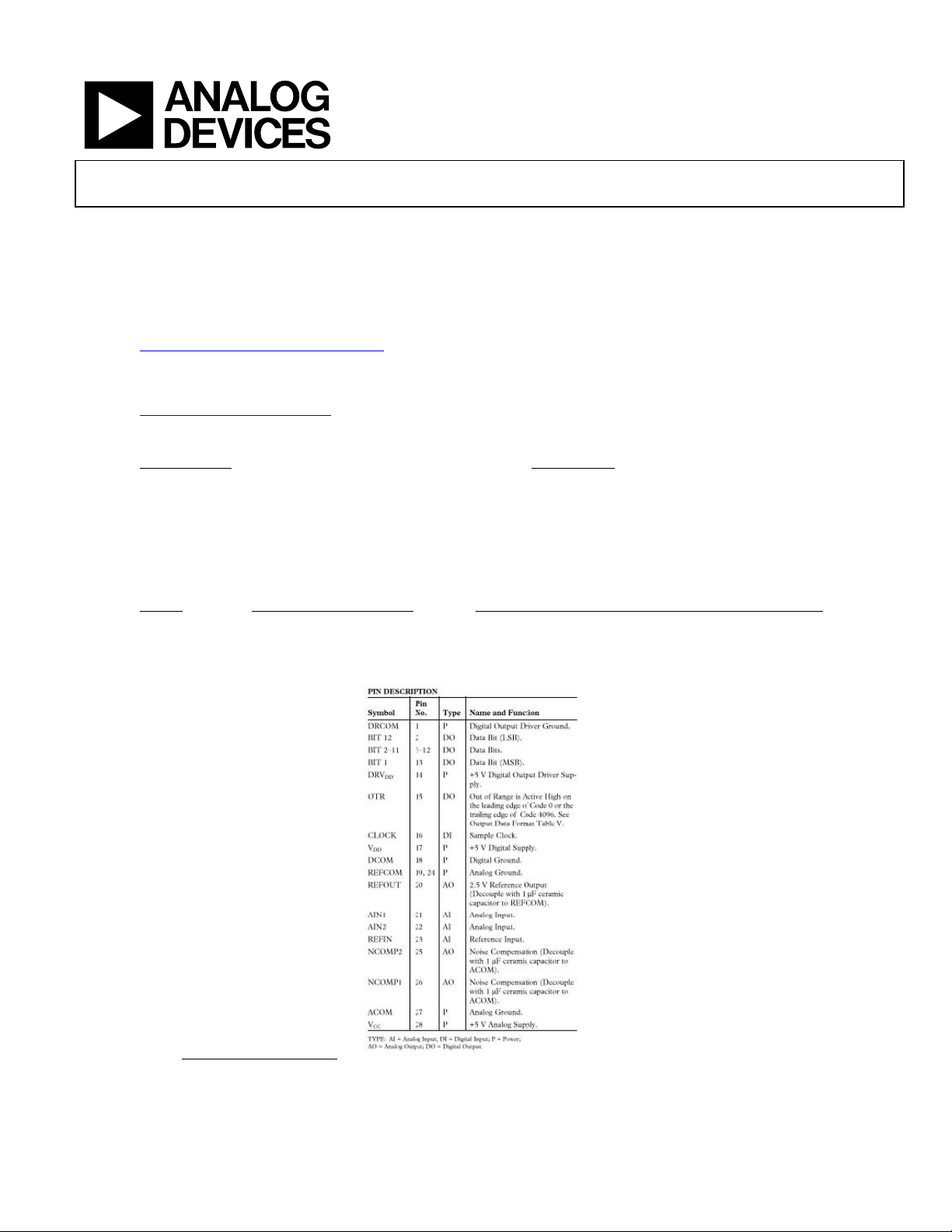
Figure 1 - Terminal connections
.
ASD0010965 Rev. G
Information furnished by Analog Devices is believed to be accurate and
reliable. However, no responsibility is assumed by Analog Devices for its use,
nor for any infringements of patents or other rights of third parties that may
result from its use. Specifications subject to change without notice. No license
is granted by implication or otherwise under any patent or patent rights of
Analog Devices. Trademarks and registered trademarks are the property of
their respective companies.
One Technology Way, P.O. Box 9106, Norwood, MA 02062-9106,
U.S.A.
Tel: 781.329.4700 www.analog.com
Fax: 781.326.8703 © 2008 Analog Devices, Inc. All rights reserved.
Page 2
AD1672
3.0 Absolute Maximum Ratings. (TA = 25°C, unless otherwise noted)
V
V
DRV
ACOM with respect to DCOM, DRCOM........................................................-0.5 to +0.5V
Clock with respect to DCOM..................................................................-0.5 to V
Digital Outputs with respect to DCOM.......................................... -0.5V to DRV
AIN with respect to ACOM ..........................................................................-6.5V to +6.5V
REFIN with respect to ACOM............................................................. -0.5V to V
Junction Temperature (T
Operating Temperature Range...................................................................-55°C to + 125°C
Storage Temperature...................................................................................-65°C to +150°C
Lead Temperature (10 sec)........................................................................................+300°C
Stresses above those listed under "Absolute Maximum Ratings" may cause permanent damage to the device. This is a stress rating
only and functional operation of the device at these or any other conditions above those indicated in the operational sections of the
specification is not implied. Exposure to absolute maximum ratings for extended periods may effect device reliability.
3.1 Thermal Characteristics:
Thermal Resistance, Sidebrazed (D) Package
Junction-to-Case (ΘJC) = 28°C/W Max
with respect to ACOM..............................................................................-0.5 to +6.5V
CC
with respect to DCOM..............................................................................-0.5 to +6.5V
DD
with respect to DRCOM .....................................................................-0.5 to +6.5V
DD
+ 0.5V
DD
+ 0.5V
DD
+ 0.5V
CC
).........................................................................................+150°C
J
Junction-to-Ambient (Θ
) = 70°C/W Max
JA
Thermal Resistance, Bottom brazed (F) Package
Junction-to-Case (Θ
Junction-to-Ambient (Θ
) = 22°C/W Max
JC
) = 60°C/W Max
JA
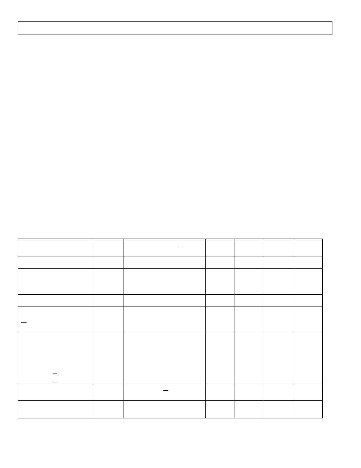
4.0 Electrical Table:
Parameter
See notes at end of table
RESOLUTION
Symbol Conditions 1/
Supply Current IVCC
IVDD
IDRVDD
Power dissipation PD
Unless Otherwise Specified
No Missing Codes 1,2,3 12
Sub
Group
1,2,3
1,2,3
Limit
Min.
Limit
Units
Max
Bits
65 mA
2
2
363 mW
Power supply rejection PSR VCC=5.0V ± 0.25V 1,2,3 -0.3 0.3 %FSR
3/
ACCURACY
Integral Nonlinearity INL
Differential Nonlinearity DNL
Offset Error VOSE
Zero Error 5/
Gain Error 2/
Internal Voltage
VO Iout = 0.5 mA 4/ 1,2,3 2.475 2.525 V
VDD=5.0V ± 0.25V
VDRDD=3.0V to 5.25V
1,2,3
-0.3 0.3
-0.1 0.1
-2.5 2.5 LSB
-1 1.5 LSB
-0.75 0.75 %FSR
-0.75 0.75 %FSR
-1.5 1.5 %FSR
Reference
Analog Input
2.5V Range Unipolar 1,2,3 0 2.5 V
5.0V Range Unipolar
0 5
ASD0010965 Rev. G | Page 2 of 5
Page 3

4.0 Electrical Table: (Cont’d)
AD1672
Parameter
See notes at end of table
Input Resistance
Output Voltage, High
Output Voltage, Low
Logic Inputs
Logic “0” Input Current
Logic “1” Input Current
AC Parameters:
Parameter
See notes at end of table
Signal to Noise Distortion
(S/(N+D))
Signal to Noise Ratio
Total Harmonic Distortion
Spurious Free Dynamic Range
NOTES:
1/
2/
3
4
5
VCC = V
DD
= V
DRVDD
Includes internal reference error.
/ Change in full scale as a function of the dc supply voltage.
/ Current available for external loads. External load should not change during conversion.
/ Bipolar Mode
Symbol Conditions 1/
Unless Otherwise Specified
Sub
Group
Limit
Min.
Limit
Max
5.0V Bipolar -2.5 2.5
2.5V Input Range
5.0V Input Range
I
V
OH
I
V
OL
I
IH
I
IL
0.5 mA 1,2,3 2.4 V
OH=
1.6 mA 1,2,3 0.4 V
OL=
V
IH=VDD
V
IL
=0V
Symbol Conditions 1/
Unless Otherwise Specified
f
=500KHz
input
SNR
THD
SFDR
f
input
f
input
f
input
=500KHz
=500KHz
=500KHz
1,2,3 1.5 3 2.5
5
1,2,3
Sub
Group
9
10,11
9
10,11
-10
Limit
Min.
63
62
66
62
10
Limit
Max
dB
9,10,11 -64 dB
9,10,11 -65 dB
= +5.0V.
Units
Kohm
uA
Units
dB
ASD0010965 Rev. G | Page 3 of 5
Page 4

AD1672
4.1 Electrical Test Requirements:
Table II
Test Requirements
Subgroups (in accordance
with MIL-PRF-38535,
Table III)
Interim Electrical Parameters 1
Final Electrical Parameters 1, 2, 3, 9, 10, 11 1/ 2/
Group A Test Requirements 1, 2, 3, 9, 10, 11
Group C end-point electrical parameters 1 2/
Group D end-point electrical parameters 1
Group E end-point electrical parameters 1
1/ PDA applies to Subgroup 1 only. No other subgroups are included in PDA.
2
/ See table III for delta parameters.
4.2 Table III. Life Test/Burn-In test delta limits.
Table III
TEST
TITLE
I
CC
V
OH
VOL
ENDPOINT
LIMIT
65
2.4
0.4
DELTA
LIMIT
±10%
±0.24
±0.1
5.0 Life Test/Burn-In Circuit:
5.1 HTRB is not applicable for this drawing.
5.2 Burn-in is per MIL-STD-883 Method 1015 test condition D.
5.3 Steady state life test is per MIL-STD-883 Method 1005.
ASD0010965 Rev. G | Page 4 of 5
UNITS
mA
V
V
Page 5

AD1672
Rev Description of Change Date
A Initiate Apr. 20, 2000
B Add Flatpack, Add radiation part number, Add timing information on
Mar. 22, 2001
page 3.
C Update web address. Feb. 7, 2002
D Change subgroups 4, 5, 6 to 9, 10, 11. Update web address Jan. 9, 2003
E Delete Burn-In circuit. Aug. 5, 2003
F Update header/footer and add to 1.0 Scope description Feb. 19,2008
Add Operating Temperature Range to Section 3.0 &
G
Remove (See Figure 2) in Sections 5.2 and 5.3
April 4, 2008
© 2008 Analog Devices, Inc. All rights reserved. Trademarks and
registered trademarks are the property of their respective
companies.
Printed in the U.S.A.
03/08
ASD0010965 Rev. G | Page 5 of 5
 Loading...