

Page 1
查询AD15452供应商
12-Bit 65 MSPS Quad A/D Converter with
FEATURES
12-bit, 65 MSPS, quad, analog-to-digital converter
Differential input with 100 Ω input impedance
Full-scale analog input: 296 mV p-p
200 MHz, 3 dB bandwidth
SNR @ −9 dBFS
64 dBFS (70 MHz AIN)
64 dBFS (140 MHz AIN)
SFDR @ −9 dBFS
81 dBFS (70 MHz AIN)
73 dBFS (140 MHz AIN)
475 mW per channel
Quad LVDS outputs
Data clock output provided
Offset binary output data format
APPLICATIONS
Antijam GPS receivers
Wireless and wired broadband communications
Communications test equipment
Integrated Signal Conditioning
AD15452
PRODUCT HIGHLIGHTS
1. Quad, 12-bit, 65 MSPS, analog-to-digital converter with
integrated analog signal conditioning optimized for antijam
global positioning system receiver (AJ-GPS) applications.
2. Packaged in a space saving 81-lead, 10 mm x 10 mm chip
scale package ball grid array (CSP_BGA) and specified over
the industrial temperature range (−40°C to +85°C).
GENERAL DESCRIPTION
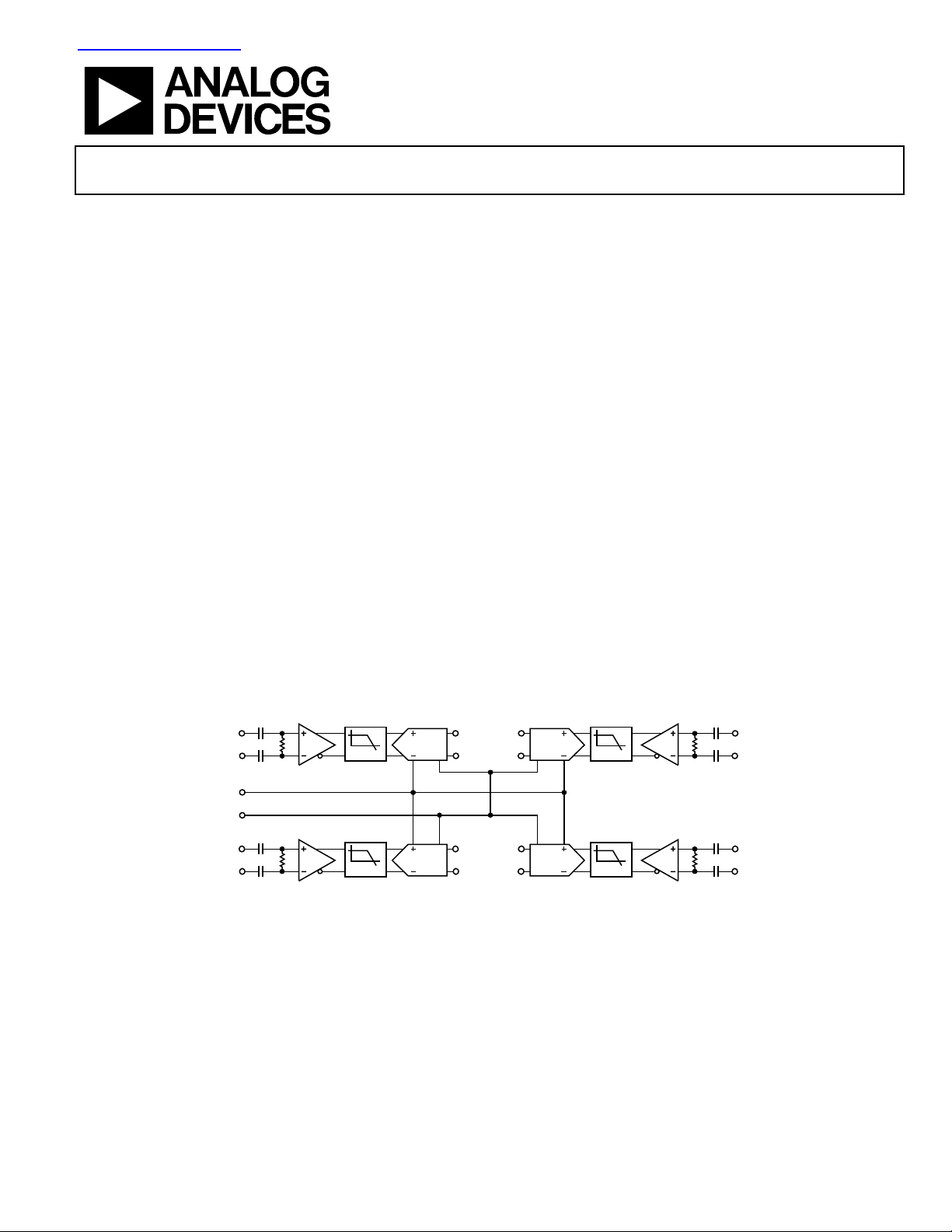
The AD15452 is a quad, 12-bit, 65 MSPS, analog-to-digital
converter (ADC). It features a differential front-end
amplification circuit followed by a sample-and-hold amplifier
and multistage pipeline analog-to-digital converter. It is
designed to operate with a 3.3 V analog supply and a 3.3 V
digital supply. Each input is fully differential. The input signals
are ac-coupled and terminated in 100 Ω input impedances. The
full-scale differential signal input range is 296 mV p-p.
Four separate 12-bit digital output signals provide data flow
from the ADCs. The digital output data is presented in offset
binary format. A single-ended clock input is used to control all
internal conversion cycles. The AD15452 is optimized for
applications in antijam global positioning receivers and is suited
for communications applications.
FUNCTIONAL BLOCK DIAGRAM
IN_A
PDOWN
CLK
IN_B
Rev. 0
Information furnished by Analog Devices is believed to be accurate and reliable. However, no
responsibility is assumed by Anal og Devices for its use, nor for any infringements of patents or ot her
rights of third parties that may result from its use. Specifications subject to change without notice. No
license is granted by implication or otherwise under any patent or patent rights of Analog Devices.
Trademarks and registered trademarks are the property of their respective owners.
LPF
LPF
D+A
D–A
D+B
D–B
Figure 1.
D+C
D–C
D+D
D–D
One Technology Way, P.O. Box 9106, Norwood, MA 02062-9106, U.S.A.
Tel: 781.329.4700 www.analog.com
Fax: 781.461.3113 © 2005 Analog Devices, Inc. All rights reserved.
LPF
LPF
IN_C
IN_D
05155-001
Page 2

AD15452
TABLE OF CONTENTS
Features.............................................................................................. 1
Typical Performance Characteristics........................................... 10
Applications....................................................................................... 1
Product Highlights ........................................................................... 1
General Description ......................................................................... 1
Functional Block Diagram .............................................................. 1
Revision History ............................................................................... 2
Specifications..................................................................................... 3
Electrical Characteristics ............................................................. 3
Timing Diagram........................................................................... 5
Absolute Maximum Ratings............................................................ 6
ESD Caution.................................................................................. 6
Pin Configuration and Function Descriptions............................. 7
Terminology ...................................................................................... 8
REVISION HISTORY
10/05—Rev. 0: Initial Version
Theory of Operation ...................................................................... 13
Analog Inputs ............................................................................. 13
Voltage Reference....................................................................... 13
Clock Input and Considerations.............................................. 13
Digital Outputs........................................................................... 13
Timing ......................................................................................... 14
DTP Pin ....................................................................................... 14
Power-Down Mode.................................................................... 14
Power Supplies............................................................................ 14
Outline Dimensions....................................................................... 15
Ordering Guide .......................................................................... 15
Rev. 0 | Page 2 of 16
Page 3

AD15452
SPECIFICATIONS
ELECTRICAL CHARACTERISTICS
@ AVDD = DRVDD = PLLVDD = 3.3 V, Encode = 65 MSPS, AIN = −9 dBFS differential input, T
Table 1.
Parameter Temp Test Level Min Typ Max Unit
RESOLUTION 12 Bits
ACCURACY
No Missing Codes Full IV Guaranteed
Offset Error 25°C I −5 +5 % FSR
Gain Error 25°C I −12.5 +12.5 % FSR
Differential Nonlinearity (DNL) Full V ±0.35 LSB
Integral Nonlinearity (INL) Full V ±0.5 LSB
TEMPERATURE DRIFT
Offset Error Full V ±10 ppm/oC
Gain Error Full V ±290 ppm/oC
MATCHING CHARACTERISTICS
Offset Error Full V ±2 % FSR
Gain Error Full V ±1.2 % FSR
INPUT REFERRED NOISE Full V 0.82 LSB rms
ANALOG INPUT
Input Range Full IV 296 mV p-p
Input Resistance
Input Capacitance
CLOCK INPUTS
High Level Input Voltage (VIH) Full IV 2 V
Low Level Input Voltage (VIL) Full IV 0.8 V
High Level Input Current (IIH) Full IV −10 +10 μA
Low Level Input Current (IIL) Full IV −10 +10 μA
Input Capacitance (CIN) Full V 2 pF
POWER-DOWN INPUT
Logic 1 Voltage Full IV 2 V
Logic 0 Voltage Full IV 0.8 V
Input Capacitance Full V 2 pF
DIGITAL OUTPUTS (LVDS)
Differential Output Voltage (VOD) Full VI 260 440 mV
Output Offset Voltage (VOS) Full VI 1.15 1.35 V
Output Coding Offset binary
CLOCK
Maximum Conversion Rate Full VI 65 MSPS
Minimum Conversion Rate Full IV 10 MSPS
Clock Pulse Width High (tEH) Full VI 6.2 ns
Clock Pulse Width Low (tEL) Full VI 6.2 ns
OUTPUT PARAMETERS
Propagation Delay (tpd) Full VI 3.3 6.5 7.9 ns
Rise Time (tR)
Fall Time (tF)
FCO Propagation Delay (t
DCO Propagation Delay (t
DCO to Data Delay (t
DCO − FCO Delay (t
Data to Data Skew Full IV ±100 ±250 ps
Wake-Up Time 25°C V 250 ns
Pipeline Latency Full IV 10 Cycles
1
1
2
2
) Full V 6.5 ns
FCO
) Full V t
DCO
) Full IV t
DATA
) Full IV t
FRAME
25°C V 100 Ω
25°C V 2.5 pF
Full V 250 ps
Full V 250 ps
+ t
FCO
/24 − 250 t
SAMPLE
/24 − 250 t
SAMPLE
Rev. 0 | Page 3 of 16
SAMPLE
SAMPLE
= 25°C, unless otherwise noted.
A
/24 ns
SAMPLE
/24 t
/24 t
/24 + 250 ps
SAMPLE
/24 + 250 ps
SAMPLE
Page 4

AD15452
Parameter Temp Test Level Min Typ Max Unit
APERTURE
Aperture Delay (tA) 25°C V 1.8 ns
Aperture Uncertainty (Jitter) 25°C <1 ps rms
POWER SUPPLIES
Supply Voltages
AVDD Full IV 3 3.3 3.6 V
DRVDD Full IV 3 3.3 3.6 V
Supply Currents
IAVDD Full I 540 592 mA
IDRVDD Full I 28 33 mA
Total Power Dissipation 25°C V 1.9 2.0 W
Power-Down Dissipation 25°C V 0.36 W
SIGNAL-TO-NOISE RATIO
f
= 70 MHz 25°C I 62.7 64.8 dBFS
INPUT
f
= 110 MHz Full V 64.7 dBFS
INPUT
f
= 140 MHz 25°C I 62.5 64.6 dBFS
INPUT
SINAD
f
= 70 MHz 25°C I 62.4 64.7 dBFS
INPUT
f
= 110 MHz Full V 64.4 dBFS
INPUT
f
= 140 MHz 25°C I 61.9 64.0 dBFS
INPUT
THD
f
= 70 MHz Full V −80.0 dBFS
INPUT
f
= 110 MHz Full V −77.0 dBFS
INPUT
f
= 140 MHz Full V −73.0 dBFS
INPUT
SPURIOUS-FREE DYNAMIC RANGE
f
= 70 MHz 25°C I 73.0 81 dBFS
INPUT
f
= 110 MHz Full V 77 dBFS
INPUT
f
= 140 MHz 25°C I 68.5 73 dBFS
INPUT
CROSSTALK Full V −60 dB
1
Input resistance and capacitance are listed as differential values.
2
Rise and fall times are defined from 20% to 80%.
Rev. 0 | Page 4 of 16
Page 5
AD15452
Table 2. Test Levels
Te st
Level
I 100% production tested.
II 100% production tested at 25°C, and sample tested at specified temperatures.
III Sample tested only.
IV Parameter is guaranteed by design and characterization testing.
V Parameter is a typical value only.
VI
TIMING DIAGRAM
Description
All devices are 100% production tested at 25°C, guaranteed by design and characterization testing for industrial temperature
range, 100% production tested at temperature extremes for military devices.
N–1
AIN
N
D10
MSB
(N – 9)
(N – 9)
05155-016
CLK
DCO–
DCO+
FCO–
FCO+
t
A
t
EH
t
CPD
t
FCO
t
D–
D+
PD
t
FRAME
MSB
D10
(N– 10)
(N– 10)D9(N– 10)D8(N– 10)D7(N– 10)D6(N– 10)D5(N– 10)D4(N– 10)D3(N– 10)D2(N– 10)D1(N– 10)D0(N– 10)
t
EL
t
DATA
Figure 2. Timing Diagram
Rev. 0 | Page 5 of 16
Page 6
AD15452
ABSOLUTE MAXIMUM RATINGS
Table 3.
Parameter Rating
AVDD to AGND −0.3 V to +3.9 V
DRVDD to DRGND −0.3 V to +3.9 V
DRGND to AGND −0.3 V to +0.3 V
DRVDD to AVDD −3.9 V to +3.9 V
Analog Inputs −0.3 V to AVDD
Digital Outputs −0.3 V to DRVDD
CLK −0.3 V to AVDD
LVDSBIAS −0.3 V to DRVDD
PDWN, DTP −0.3 V to AVDD
Operational Case Temperature −40°C to +85°C
Storage Temperature Range 65°C to 150°C
Lead Temperature:
Infrared, 15 seconds
230°C
Stresses above those listed under Absolute Maximum Ratings
may cause permanent damage to the device. This is a stress
rating only; functional operation of the device at these or any
other conditions above those indicated in the operational
section of this specification is not implied. Exposure to absolute
maximum rating conditions for extended periods may affect
device reliability.
ESD CAUTION
ESD (electrostatic discharge) sensitive device. Electrostatic charges as high as 4000 V readily accumulate on
the human body and test equipment and can discharge without detection. Although this product features
proprietary ESD protection circuitry, permanent damage may occur on devices subjected to high energy
electrostatic discharges. Therefore, proper ESD precautions are recommended to avoid performance
degradation or loss of functionality.
Rev. 0 | Page 6 of 16
Page 7

AD15452
PIN CONFIGURATION AND FUNCTION DESCRIPTIONS
876
9
BOTTOM VIEW
(Not to S cale)
Figure 3. Pin Configuration
Table 4. Pin Function Descriptions
Pin No. Mnemonic Description
A2 VIN+A Channel A Positive Analog Input.
A1 VIN−A Channel A Negative Analog Input.
B2 VIN+B Channel B Positive Analog Input.
B1 VIN−B Channel B Negative Analog Input.
H2 VIN+C Channel C Positive Analog Input.
H1 VIN−C Channel C Negative Analog Input.
J2 VIN+D Channel D Positive Analog Input.
J1 VIN−D Channel D Negative Analog Input.
E8 D+A ADC A True Digital Out.
E9 D−A ADC A Complement Digital Out.
F8 D+B ADC B True Digital Out.
F9 D−B ADC B Complement Digital Out.
G8 D+C ADC C True Digital Out.
G9 D−C ADC C Complement Digital Out.
H8 D+D ADC D True Digital Out.
H9 D−D ADC D Complement Digital Out.
J6 CLK Clock Input.
A7 PDWN Power-Down Function Selection.
B3, C3, D2, E1, E2, F2, F3, F4, G3, G4, H3
AVDD Analog Power Supply Connection.
H7, J7
A3, A4, A5, A6, B4, B5, B6, C1, C2, C4, C5,
AGND Analog Ground Connection.
D1, D5, E5, F1, F5 G1, G2, G5, H4, H5, H6,
J3, J4, J5
A8, A9, B8, B9, DRVDD Digital Output Driver Supply Connection.
C6, C7, D6, D7, E6, E7, F6, F7, G6, G7, J8 DRGND Digital Output Ground Connection.
D3 VREF Voltage Reference Input/Output.
D4 SENSE Reference Mode Selection.
E4 REFT Differential Reference (Top).
E3 REFB Differential Reference (Bottom).
C8 DCO+ Data Clock Output; True.
C9 DCO− Data Clock Output; Complement.
D8 FCO+ Frame Clock Indicator; True.
D9 FCO− Frame Clock Indicator Output; Complement.
B7 DTP Digital Test Pattern Enable.
J9 LVDSBIAS LVDS Output Current Set Resistor Pin.
Rev. 0 | Page 7 of 16
3
5
1
2
4
A
B
C
D
E
F
G
H
J
05155-002
Page 8

AD15452
TERMINOLOGY
Analog Bandwidth
Analog bandwidth is the analog input frequency at which the
spectral power of the fundamental frequency (as determined by
the FFT analysis) is reduced by 3 dB from full scale.
Aperture Delay
Aperture delay is a measure of the sample-and-hold amplifier
(SHA) performance and is measured from the 50% point rising
edge of the clock input to the time at which the input signal is
held for conversion.
Aperture Uncertainty (Jitter)
Aperture jitter is the variation in aperture delay for successive
samples and can be manifested as frequency dependent noise
on the ADC input.
Clock Pulse Width and Duty Cycle
Pulse width high is the minimum amount of time that the clock
pulse should be left in the Logic 1 state to achieve a rated
performance. Pulse width low is the minimum time the clock
pulse should be left in the low state. At a given clock rate, these
specifications define an acceptable clock duty cycle.
Common-Mode Rejection Ratio (CMRR)
CMRR is defined as the amount of rejection on the differential
analog inputs over the entire full-scale signal range.
Crosstalk
Crosstalk is defined as the coupling onto any other channel
when one channel is driven by a full-scale signal.
Gain Flatness
Gain flatness is the measured amount of fluctuation in the
analog front-end input response to the bandwidth measured.
Differential Analog Input Capacitance
The complex impedance simulated at each analog input port.
Differential Analog Input Voltage Range
The peak-to-peak differential voltage that must be applied to
the converter to generate a full-scale response. Peak differential
voltage is computed by observing the voltage on a pin and
subtracting the voltage from a second pin that is 180° out of
phase. Peak-to-peak differential is computed by rotating the
input phase 180° and taking the peak measurement again. The
difference is computed between both peak measurements.
Differential Nonlinearity (DNL, No Missing Codes)
An ideal ADC exhibits code transitions that are exactly 1 LSB
apart. DNL is the deviation from this ideal value. Guaranteed
no missing codes to an n-bit resolution indicates that all 2
n
codes, respectively, must be present over all operating ranges.
Effective Number of Bits (ENOB)
For a sine wave, SINAD can be expressed in terms of the
number of bits. Using the following formula, it is possible to
obtain a measure of performance expressed as N, the effective
number of bits:
N = (SINAD – 1.76)/6.02
Thus, the effective number of bits for a device for sine wave
inputs at a given input frequency can be calculated directly
from its measured SINAD.
Gain Error
The largest gain error is specified and is considered the
difference between the measured and ideal full-scale input
voltage range.
Gain Matching
Expressed in %FSR. Computed using the following equation:
−
FSRFSR
MatchingGain
=
⎛
⎜
⎝
minmax
minmax
+
FSRFSR
⎞
2
⎟
⎠
%100
×
where:
FSR
is the most positive gain error of the ADCs.
MAX
FSR
is the most negative gain error of the ADCs.
MIN
Second and Third Harmonic Distortion
The ratio of the rms signal amplitude to the rms value of the
second or third harmonic component, reported in dBc.
Integral Nonlinearity (INL)
INL refers to the deviation of each individual code from a line
drawn from negative full scale through positive full scale. The
point used as negative full scale occurs 1/2 LSB before the first
code transition. Positive full scale is defined as a level 1 1/2 LSB
beyond the last code transition. The deviation is measured from
the middle of each particular code to the true straight line.
Noise Power Ratio (NPR)
NPR is the rms noise power injected into the ADC vs. the
rejected band of interest (notch depth measured).
Offset Error
The largest offset error is specified and is considered the
difference between the measured and ideal voltage at the analog
input that produces the midscale code at the outputs.
Rev. 0 | Page 8 of 16
Page 9

AD15452
Offset Matching
Expressed in mV. Computed using the following equation:
OffsetMatching = OFF
MAX
− OFF
MIN
where:
is the most positive offset error.
OFF
MAX
OFF
is the most negative offset error.
MIN
Out-of-Range Recovery Time
Out-of-range recovery time is the time it takes for the ADC to
reacquire the analog input after a transient from 10% above
positive full scale to 10% above negative full scale, or from 10%
below negative full scale to 10% below positive full scale.
Output Propagation Delay
The delay between the clock logic threshold and the time when
all bits are within valid logic levels.
Power Supply Rejection Ratio (PSRR)
PSRR is the measure of change in a given supply relative to the
amount of error seen on the ADC reconstructed output. This is
measured in decibels based on the spurious feedthrough of the
device.
Signal-to-Noise and Distortion (SINAD) Ratio
SINAD is the ratio of the rms value of the measured input
signal to the rms sum of all other spectral components below
the Nyquist frequency, including harmonics but excluding dc.
The value for SINAD is expressed in decibels.
Signal-to-Noise Ratio (SNR)
SNR is the ratio of the rms value of the measured input signal to
the rms sum of all other spectral components below the Nyquist
frequency, excluding the first six harmonics and dc. The value
for SNR is expressed in decibels.
Spurious-Free Dynamic Range (SFDR)
SFDR is the difference in dB between the rms amplitude of the
input signal and the peak spurious signal.
Tem p er at u re Dr i ft
The temperature drift for offset error and gain error specifies
the maximum change from the initial (25°C) value to the value
at T
MIN
or T
MAX
.
Two -Tone SFDR
The ratio of the rms value of either input tone to the rms value
of the peak spurious component. The peak spurious component
can be an IMD product. It may be reported in dBc (that is,
degrades as signal levels are lowered) or in dBFS (always related
back to converter full scale).
Rev. 0 | Page 9 of 16
Page 10

AD15452
TYPICAL PERFORMANCE CHARACTERISTICS
0
–1
–2
–3
–4
–5
ROLL-OFF (dB)
–6
–7
–8
–9
10 100
Figure 4. Analog Input Bandwidth
0
10
20
30
40
50
60
70
80
MAGNITUDE (dB)
90
100
110
120
130
1
9.756.503.25 13.00
Figure 5. FFT Plot with f
0
10
20
30
40
50
60
70
80
MAGNITUDE (dB)
90
100
110
120
130
3
Figure 6. FFT Plot with f
FREQUENCY (M Hz )
2
3
FREQUENCY ( M Hz )
6
4
FREQUENCY ( M Hz )
4
= 70 MHz
IN
1
= 110 MHz
IN
1000
05155-003
5
6
26.0022.75 29.25 32.5019.5016.250
05155-012
2
26.0022.75 29.25 32.5019.5016.2509.756.503.25 13.00
5
05155-013
0
10
20
30
40
50
60
70
80
MAGNITUDE (dB)
90
6
100
110
120
130
11.00
10.75
10.50
10.25
10.00
9.75
9.50
ATTENUATION (dB)
9.25
9.00
8.75
8.50
–5 0 5 10 15 20 25 30
1
5
FREQUENCY ( M Hz )
Figure 7. FFT Plot with f
IF = 70
IF = 110
IF = 140
FREQUENCY (M Hz )
IN
Figure 8. Gain Flatness 30 MHz Centered @ IF
0
–10
–20
–30
–40
–50
CROSSTALK (dB)
–60
–70
–80
–90
10 100
FREQUENCY (M Hz )
Figure 9. Typical Crosstalk
2
4
26.0022.75 29.25 32.5019.5016.2509.756.503.25 13.00
= 140 MHz
3
35
1000
05155-014
05155-004
05155-005
Rev. 0 | Page 10 of 16
Page 11

AD15452
90
85
80
75
70
SFDR (dBFS)
65
60
55
–16 –15 –14 –13 –12 –11–10 –9 –8 –7 –6 –5 –4 –3 –2 –1
BACK-OFF (d BFS)
Figure 10. SFDR vs. Backoff @ AIN with f
90
85
80
75
70
SFDR (dBFS)
65
60
55
–16 –15 –14 –13 –12 –11–10 –9 –8 –7 –6 –5 –4 –3 –2 –1
BACK-OFF (d BFS)
Figure 11. SFDR vs. Backoff @ AIN with f
90
= 70 MHz
IN
= 110 MHz
IN
0
05155-006
0
05155-007
86
84
82
80
78
76
74
72
SNR/SFDR (dBFS)
70
68
66
64
62
–40 25 85
SFDR = 70MHz
SFDR = 110MHz
SFDR = 140MHz
SNR = 70MHz/ 110MHz/140MHz
TEMPERATURE (°C)
Figure 13. SNR/SFDR vs. Temperature with F
0.5
0.4
0.3
0.2
0.1
0
INL (LSB)
–0.1
–0.2
–0.3
–0.4
–0.5
1024 15365120 2048 2560 409635843072
CODE
Figure 14. Typical INL
@ −9 dBFS
IN
05155-009
05155-010
85
80
75
70
SFDR (dBFS)
65
60
55
–16 –15 –14 –13 –12 –11–10 –9 –8 –7 –6 –5 –4 –3 –2 –1
BACK-OFF (d BFS)
Figure 12. SFDR vs. Backoff @ AIN with f
= 140 MHz
IN
0
05155-008
Rev. 0 | Page 11 of 16
Page 12

AD15452
75
0.2
0.1
0
DNL (LSB)
–0.1
–0.2
1024 15365120 2048 2560 409635843072
CODE
05155-011
Figure 15. Typical DNL
70
65
60
55
50
CMRR (dB)
45
40
35
30
10 100
Figure 16. Common-Mode Rejection Ratio
FREQUENCY (M Hz )
1000
05155-015
Rev. 0 | Page 12 of 16
Page 13

AD15452
THEORY OF OPERATION
The AD15452 consists of four high performance ADC
channels. Each channel is independent of each other with the
exception of a shared internal reference source, VREF, and
sample clock. The channels consist of a differential front-end
amplification circuit followed by a low-pass filter and a multistage pipeline ADC. The quantized outputs from each stage are
combined into a 12-bit result. The output staging block aligns
the data, carries out the error correction, and passes the data to
the output buffers; the data is then serialized and aligned to the
frame and output clock.
ANALOG INPUTS
Each analog input is fully differential, allowing sampling of
differential input signals. The differential input signals are accoupled and terminated in 100 Ω input impedances. The fullscale differential signal input range is 296 mV p-p.
VOLTAGE REFERENCE
The AD15452 reference voltage is set internally to 0.5 V. The
VREF pin and SENSE pin are used to decouple the 0.5 V
reference. The VREF pin and SENSE pin must be shorted
together and then decoupled with a 10 F capacitor to AGND.
Ideally, this capacitor should be placed as close to the pins as
possible. The REFT pin and the REFB pin must have a 10 F
capacitor placed between the two pins.
CLOCK INPUT AND CONSIDERATIONS
Typical high speed ADCs use both clock edges to generate a
variety of internal timing signals, and as a result may be
sensitive to clock duty cycle. Typically, a 5% tolerance is
required on the clock duty cycle to maintain dynamic performance characteristics. The AD15452 has a self-contained clock
duty cycle stabilizer that retimes the nonsampling edge,
providing an internal clock signal with a nominal 50% duty
cycle. This allows a wide range of clock input duty cycles
without affecting the performance of the AD15452.
An on-board phase-locked loop (PLL) multiplies the input
clock rate for shifting the serial data out. Consequently, any
change to the sampling frequency requires a minimum of 100
clock periods to allow the PLL to reacquire and lock to the
new rate.
High speed, high resolution ADCs are sensitive to the quality of
the clock input. The degradation in SNR at a given full-scale
input frequency (f
calculated with the following equation:
SNR degradation = 20 × log10 [1/2 × π × f
) due only to aperture jitter (tA) can be
A
× tA]
A
In the equation, the rms aperture jitter, t
, represents the root
A
sum square of all jitter sources, which include the clock input,
analog input signal, and ADC aperture jitter specification.
Applications that require undersampling are particularly
sensitive to jitter.
The clock input is treated as an analog signal in cases where
aperture jitter can affect the dynamic range of the AD15452.
Power supplies for clock drivers are separated from the ADC
output driver supplies to avoid modulating the clock signal with
digital noise. Low jitter, crystal-controlled oscillators make the
best clock sources. If the clock is generated from another type of
source (by gating, dividing, or other methods) then the original
clock at the last step should retime it.
DIGITAL OUTPUTS
The AD15452 differential outputs conform to the ANSI-644
LVDS standard. To set the LVDS bias current, place a resistor
(RSET is nominally equal to 4.0 kΩ) to ground at the
LVDSBIAS pin. The RSET resistor current is derived on-chip
and sets the output current at each output equal to a nominal
3.5 mA. A 100 Ω differential termination resistor placed at the
LVDS receiver inputs results in a nominal 350 mV swing at the
receiver. To adjust the differential signal swing, simply change
the resistor to a different value, as shown in
Table 5. LVDSBIAS Differential Output Swing
RSET Differential Output Swing
3.6 kΩ 375 mV p-p
3.9 kΩ (Default) 350 mV p-p
4.3 kΩ 325 mV p-p
The AD15452 LVDS outputs facilitate interfacing with LVDS
receivers in custom ASICs and FPGAs that have LVDS capability for superior switching performance in noisy environments.
Single point-to-point net topologies are recommended with a
100 Ω termination resistor placed as close to the receiver as
possible. It is recommended to keep the trace length no longer
than 12 inches and to keep differential output traces close
together and at equal lengths.
The format of the output data can be selected as offset binary. A
quick example of the output coding format can be found in
Tabl e 6 .
Table 6. Digital Output Coding
Code
4095 0.147 1111 1111 1111
2048 0 1000 0000 0000
2047 −0.000072 0111 1111 1111
0 −0.148 0000 0000 0000
(VIN+) − (VIN−) Input
Span = 296 V p-p (V)
Tabl e 5 .
Digital Output Offset
Binary (D11...D0)
Rev. 0 | Page 13 of 16
Page 14

AD15452
TIMING
Data from each ADC is serialized and provided on a separate
channel. The data rate for each serial stream is equal to 12 bits
times the sample clock rate, with a maximum of 780 MHz
(12 bits × 65 MSPS = 780 MHz). The lowest typical conversion rate
is 10 MSPS.
POWER-DOWN MODE
By asserting the PDWN pin high, the AD15452 is placed in
power-down mode with a typical power dissipation of 360 mW.
During power-down, the LVDS output drivers are placed in a
high impedance state. To return the AD15452 to normal
operating mode, reassert the PDWN pin low.
Two output clocks are provided to assist in capturing data from
the AD15452. The DCO is used to clock the output data and is
equal to six times the sampling clock (CLK) rate. Data is
clocked out of the AD15452 and can be captured on the rising
and falling edges of the DCO that supports double-data rate
(DDR) capturing. The frame clock out (FCO) is used to signal
the start of a new output byte and is equal to the sampling clock
rate. See the timing diagram shown in
information.
Figure 2 for more
DTP PIN
The digital test pattern (DTP) pin can be enabled for two different
types of test patterns. When the DTP is tied to AVDD/3, all the
ADC channel outputs shift out the 1000 0000 0000 pattern. When
the DTP is tied to 2 × AVDD/3, all the ADC channel outputs shift
out the 1010 1010 1010 pattern. The FCO and DCO outputs still
work as usual while all channels shift out the test pattern. This
pattern allows the user to perform timing alignment adjustments
between the DCO and the output data. For normal operation, this
pin should be grounded to AGND.
In power-down mode, low power dissipation is achieved by
shutting down the reference, reference buffer, PLL, and biasing
networks. The decoupling capacitors on REFT and REFB are
discharged when entering standby mode and then must be
recharged when returning to normal operation. As a result, the
wake-up time is related to the time spent in the power-down
mode and shorter cycles result in proportionally shorter wakeup times. With the recommended 0.1 µF and 10 µF decoupling
capacitors on REFT and REFB, it takes approximately one
second to fully discharge the reference buffer decoupling
capacitors and 3 ms to restore full operation.
POWER SUPPLIES
The nominal setting for the AVDD, PLLVDD, and DRVDD
supplies is 3.3 V. The AVDD and PLLVDD supplies (analog)
should be kept separate from the DRVDD supply (digital).
AVDD and PLLVDD can be tied together as long as clean
supplies are used.
Power supply decoupling capacitors should be used to decouple
the supplies at the board connections. Internal decoupling is
present in the AD15452 and any external decoupling capacitors
should be placed as close to the AD15452 supply pins as
possible.
Both the analog and digital ground pins are used to dissipate
power from the AD15452’s package. These ground pins should
be brought to a ground plane in order to maximize the thermal
dissipation designed into the package.
Table 7. Digital Test Pattern Pin Settings
Selected DTP DTP Voltage Resulting D1+, D1– Resulting FCO and DCO
Normal Operation AGND Normal operation Normal operation
DTP1 AVDD/3 1000 0000 0000 Normal operation
DTP2 2 × AVDD/3 1010 1010 1010 Normal operation
Restricted AVDD NA NA
Rev. 0 | Page 14 of 16
Page 15

AD15452
OUTLINE DIMENSIONS
A1 CORNER
INDEX AREA
5
4
BOTTOM VIEW
DETAILA
0.70
SEATING
0.60
PLANE
0.50
1
2
1.10
0.25
A
B
C
D
E
F
G
H
J
0.20
COPLANARITY
1.70 MAX
10.00
BSC SQ
BALL A1
INDICATOR
TOP VIEW
DETAIL A
COMPLIANT WITH JEDEC STANDARDS MO-192-ABC-1.
8.00
BSC SQ
0.30 MIN
BSC
1.00
9
876 3
BALL DIAMETER
Figure 17. 81-Lead Chip Scale Package Ball Grid Array [CSP_BGA]
(BC-81-1)
Dimensions shown in millimeters
ORDERING GUIDE
Model Temperature Range Package Description Package Option
AD15452BBC −40°C to +85°C 81-Lead Chip Scale Package Ball Grid Array (CSPBGA) BC-81-1
AD15452/PCB Evaluation Board
Rev. 0 | Page 15 of 16
Page 16

AD15452
NOTES
© 2005 Analog Devices, Inc. All rights reserved. Trademarks and
registered trademarks are the property of their respective owners.
D05155-0-10/05(0)
Rev. 0 | Page 16 of 16
Page 17

Page 18

Page 19

Page 20

 Loading...