

Page 1
A
www.BDTIC.com/ADI
12-Bit, 65 MSPS, Dual ADC
FEATURES
12-bit, 65 MSPS dual ADC
Differential input with 100 Ω input impedance
Full-scale analog input: 296 mV p-p
170 MHz, 3 dB bandwidth
SNR (−9 dBFS): 64 dBFS (70 MHz AIN), 64 dBFS (140 MHz AIN)
SFDR (−9 dBFS): 77 dBFS (70 MHz AIN), 73 dBFS (140 MHz AIN)
435 mW per channel
Dual parallel output buses
Out-of-range indicators
Independent clocks
Duty cycle stabilizer
OBSOLETE
Twos complement or offset binary data format
APPLICATIONS
Antijam GPS receivers
Wireless and wired broadband communications
Communications test equipment
OTR_A
PDWN
OEB_A
PDWNB
OEB_B
OTR_B
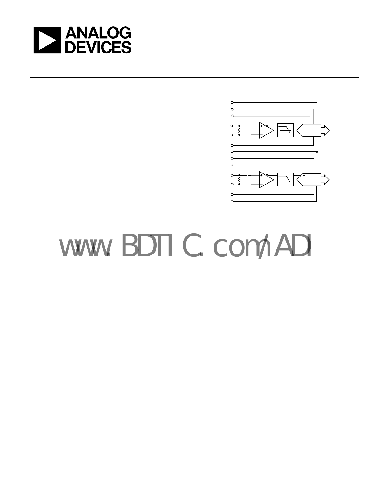
FUNCTIONAL BLOCK DIAGRAM
CLKA
INA
DFS
CLKB
INB
LPF
LPF
Figure 1.
AD15252
AD15252
DATA
BUS A
DATA
BUS B
05154-001
GENERAL DESCRIPTION
The AD15252 is a dual, 12-bit, 65 MSPS, analog-to-digital
converter (ADC). It features a differential front-end
amplification circuit followed by a sample-and-hold amplifier
and multistage pipeline ADC. It is designed to operate with a
3.3 V analog supply and a 2.5 V/3.3 V digital supply. Each input
is fully differential, ac-coupled, and terminated in 100 Ω input
impedances. The full-scale differential signal input range is
296 mV p-p.
Two parallel, 12-bit digital output buses provide data flow from
t
he ADCs. The digital output data is presented in either straight
binary or twos complement format. Out-of-range (OTR) signals
indicate an overflow condition, which can be used with the
most significant bit to determine low or high overflow. Dual
single-ended clock inputs control all internal conversion cycles.
A duty cycle stabilizer allows wide variations in the clock duty
cycle while maintaining excellent performance. The AD15252 is
optimized for applications in antijam global positioning
receivers and is well suited for communications applications.
PRODUCT HIGHLIGHTS
1. Dual 12-bit, 65 MSPS ADC with integrated analog signal
conditioning optimized for antijam global positioning
system receiver (AJ-GPS) applications.
perates from a single 3.3 V power supply and features a
2. O
separate digital output driver supply to accommodate 2.5 V
and 3.3 V logic families.
ackaged in a space-saving 8 mm × 8 mm chip scale
3. P
package ball grid array (CSP_BGA) and is specified over
the industrial temperature range (–40°C to +85°C).
Rev. 0
Information furnished by Analog Devices is believed to be accurate and reliable.
However, no responsibility is assumed by Analog Devices for its use, nor for any
infringements of patents or other rights of third parties that may result from its use.
Specifications subject to change without notice. No license is granted by implication
or otherwise under any patent or patent rights of Analog Devices. Trademarks and
registered trademarks are the property of their respective owners.
One Technology Way, P.O. Box 9106, Norwood, MA 02062-9106, U.S.A.
Tel: 781.329.4700 www.analog.com
Fax: 781.461.3113 © 2005 Analog Devices, Inc. All rights reserved.
Page 2

AD15252
www.BDTIC.com/ADI
TABLE OF CONTENTS
Electrical Characteristics................................................................. 3
Clock Input and Considerations .............................................. 11
Absolute Maximum Ratings............................................................ 5
ESD Caution.................................................................................. 5
Pin Configuration and Function Descriptions............................. 6
Typical Performance Characteristics ............................................. 8
Theory of Operation ...................................................................... 11
Analog Input ............................................................................... 11
Volt a ge R e fe r e nc e ....................................................................... 11
OBSOLETE
REVISION HISTORY
8/05—Revision 0: Initial Version
Power Dissipation and Standby Mode .................................... 11
Digital Outputs........................................................................... 12
Timing ......................................................................................... 12
Data Format ................................................................................ 12
PCB and Evaluation Board............................................................ 13
Outline Dimensions ....................................................................... 19
Ordering Guide .......................................................................... 19
Rev. 0 | Page 2 of 20
Page 3
AD15252
www.BDTIC.com/ADI
ELECTRICAL CHARACTERISTICS
AVDD = 3.3 V, DRVDD = 2.5 V, encode = 65 MSPS, CLK_A = CLK_B, AIN = −9 dBFS differential input, TA= 25°C, unless otherwise
noted.
Table 1.
Parameter Temp Test Level Min Typ Max Unit
RESOLUTION 12 Bits
ACCURACY
No Missing Codes 25°C IV Guaranteed
Offset Error 25°C I −6 ±1.7 +6 % FSR
Gain Error 25°C I −12.5 ±2.0 +12.5 % FSR
Differential Nonlinearity (DNL) Full V ±0.35 LSB
Integral Nonlinearity (INL) Full V ±0.8 LSB
TEMPERATURE DRIFT
Offset Error Full V ±9 ppm/°C
Gain Error Full V ±172 ppm/°C
MATCHING CHARACTERISTICS
OBSOLETE
Offset Error Full V ±2.0 % FSR
Gain Error Full V ±1.0 % FSR
Input Referred Noise Full V 0.87 LSB rms
ANALOG INPUT
Input Range Full IV 296 mV p-p
Input Resistance (RIN)
Input Capacitance (CIN)
CLOCK INPUTS
High Level Input Voltage (VIH) Full IV 2.0 V
Low Level Input Voltage (V
High Level Input Current (IIH) Full IV −10 +10 μA
Low Level Input Current (IIL) Full IV −10 +10 μA
Input Capacitance (CIN) Full V 2 pF
LOGIC OUTPUTS
High Level Output Voltage (VOH) Full IV 2.49 V
Low Level Output Voltage (VOL) Full IV 0.2 V
INTERFACE TIMING
Maximum Conversion Rate Full VI 65 MSPS
Minimum Conversion Rate Full IV 1 MSPS
Clock Period (tC) Full V 15.4 ns
Clock Width High (tCH) Full IV 6.2 ns
Clock Width Low (tCL) Full IV 6.2 ns
Clock to Data (tOD) Full IV 2 6 ns
Pipeline Delay (Latency) Full V 7 Cycles
POWER SUPPLIES
Supply Voltages
AVDD Full IV 3.0 3.3 3.6 V
DRVDD Full IV 2.25 2.5 3.6 V
Supply Currents
AVDD Full VI 254 280 mA
DRVDD Full VI 12 15 mA
Total Power Dissipation Full VI 0.87 1.0 W
1
1
IL)
25°C V 100 Ω
25°C V 1.8 pF
Full IV 0.8 V
Rev. 0 | Page 3 of 20
Page 4

AD15252
www.BDTIC.com/ADI
Parameter Temp Test Level Min Typ Max Unit
SIGNAL-TO-NOISE RATIO (SNR)
f
= 70 MHz 25°C I 62.7 64.2 dBFS
INPUT
f
= 110 MHz 25°C V 64.1 dBFS
INPUT
f
= 140 MHz 25°C I 62.5 64 dBFS
INPUT
SINAD
f
= 70 MHz 25°C I 62.4 63.9 dBFS
INPUT
f
= 110 MHz 25°C V 63.7 dBFS
INPUT
f
= 140 MHz 25°C I 61.9 63.3 dBFS
INPUT
THD
f
= 70 MHz Full V −76 dBFS
INPUT
f
= 110 MHz Full V −74 dBFS
INPUT
f
= 140 MHz Full V −72 dBFS
INPUT
SPURIOUS-FREE DYNAMIC RANGE (SFDR)
f
= 70 MHz 25°C I 72.7 77.8 dBFS
INPUT
f
= 110 MHz 25°C V 75.9 dBFS
INPUT
f
= 140 MHz 25°C I 68 73.8 dBFS
INPUT
OBSOLETE
CROSSTALK 25°C V −70 dB
1
Input resistance and capacitance shown as differential.
Table 2. Explanation of Test Levels
Test Level Description
I 100% production tested.
II 100% production tested at 25°C, and sample tested at specified temperatures.
III Sample tested only.
IV Parameter is guaranteed by design and characterization testing.
V Parameter is a typical value only.
VI
All devices are 100% production tested at 25°C, guaranteed by design and characterization testing for industrial
ature range; 100% production tested at temperature extremes for military devices.
temper
Rev. 0 | Page 4 of 20
Page 5

AD15252
www.BDTIC.com/ADI
ABSOLUTE MAXIMUM RATINGS
Table 3.
Parameter Rating
AVDD to AGND −0.3 V, +3.9 V
DRVDD to DRGND −0.3 V, +3.9 V
DRGND to AGND −0.3 V, +0.3 V
DRVDD to AVDD −3.9 V, +3.9 V
Analog Inputs −0.3 V, AVDD + 0.3 V
Digital Outputs −0.3 V, DRVDD + 0.3 V
CLK −0.3 V, AVDD + 0.3 V
Operational Case Temperature −40°C to 85°C
Storage Temperature Range −65°C to 150°C
Lead Temperature: Infrared, 15 sec 230°C
OBSOLETE
ESD CAUTION
ESD (electrostatic discharge) sensitive device. Electrostatic charges as high as 4000 V readily accumulate on
the human body and test equipment and can discharge without detection. Although this product features
proprietary ESD protection circuitry, permanent damage may occur on devices subjected to high energy
electrostatic discharges. Therefore, proper ESD precautions are recommended to avoid performance
degradation or loss of functionality.
Stresses above those listed under Absolute Maximum Ratings
may cause permanent damage to the device. This is a stress
rating only; functional operation of the device at these or any
other conditions above those indicated in the operational
section of this specification is not implied. Exposure to absolute
maximum rating conditions for extended periods may affect
device reliability.
Rev. 0 | Page 5 of 20
Page 6
AD15252
www.BDTIC.com/ADI
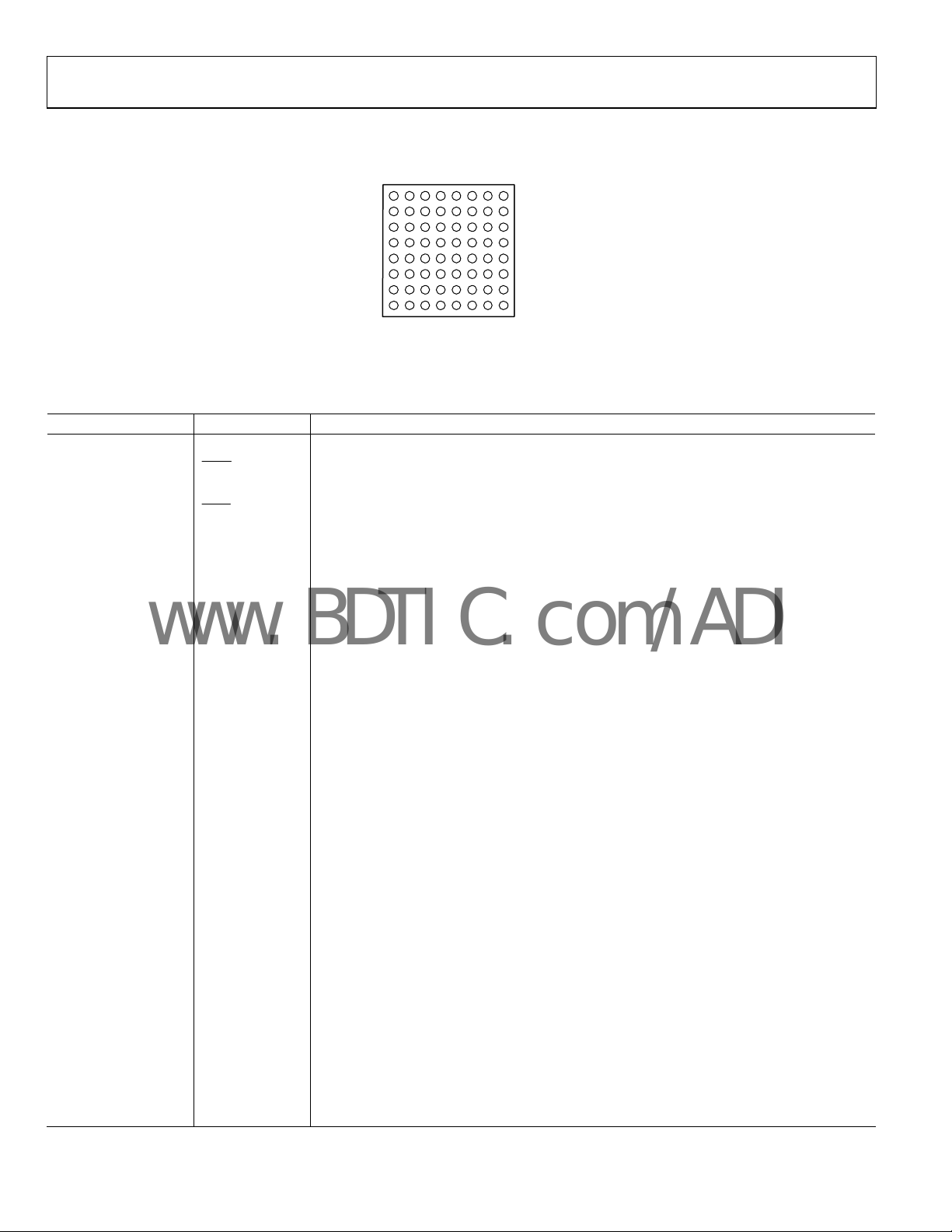
PIN CONFIGURATION AND FUNCTION DESCRIPTIONS
87654321
Figure 2. Pin Configuration
Table 4. Pin Function Descriptions
Pin No. Mnemonic Description
A1 VINA Analog Input Pin (+) for Channel A.
OBSOLETE
A2 VINA Analog Input Pin (−) for Channel A.
H1 VINB
H2
B4 CLK_A
G4 CLK_B Clock Input Pin for Channel B.
C4 PDWN_A Power-Down Function Selection for Channel A (Active High).
F4 PDWN_B Power-Down Function Selection for Channel B (Active High).
A4 OTR_A Out-of-Range Indicator for Channel A.
E8 OTR_B Out-of-Range Indicator for Channel B.
A3 VCM_A Channel A Common Mode.
H3 VCM_B Channel B Common Mode.
D4 OEB_A Output Enable for Channel A. Logic 0 enables Data Bus A; Logic 1 sets outputs to high-Z.
E4 OEB_B Output Enable for Channel B. Logic 0 enables Data Bus B; Logic 1 sets outputs to high-Z.
C5 D11_A(MSB) Channel A Data Output Bit 11 (MSB).
A5 D10_A Channel A Data Output Bit 10.
B5 D09_A Channel A Data Output Bit 9.
A6 D08_A
B6 D07_A Channel A Data Output Bit 7.
A7 D06_A
B7 D05_A
A8 D04_A
C6 D03_A
B8 D02_A
C7 D01_A Channel A Data Output Bit 1.
C8 D00_A(LSB)
E3 DFS
E7 D11_B(MSB)
F8 D10_B Channel B Data Output Bit 10.
F7 D09_B
G8 D08_B Channel B Data Output Bit 8.
VINB
Analog Input Pin (+) for Channel B.
Analog Input Pin (−) for Channel B.
Clock Input Pin for Channel A.
Channel A Data Output Bit 8.
Channel A Data Output Bit 6.
Channel A Data Output Bit 5.
Channel A Data Output Bit 4.
Channel A Data Output Bit 3.
Channel A Data Output Bit 2.
Channel A Data Output Bit 0 (LSB).
Data Output Format Select Bit (Logic 0 for offset binary, Logic 1 for twos complement).
Channel B Data Output Bit 11 (MSB).
Channel B Data Output Bit 9.
BOTTOM VIEW
(Not to Scale)
A
B
C
D
E
F
G
H
05154-003
Rev. 0 | Page 6 of 20
Page 7

AD15252
www.BDTIC.com/ADI
Pin No. Mnemonic Description
F6 D07_B Channel B Data Output Bit 7.
H8 D06_B Channel B Data Output Bit 6.
G7 D05_B Channel B Data Output Bit 5.
H7 D04_B Channel B Data Output Bit 4.
G6 D03_B Channel B Data Output Bit 3.
H6 D02_B Channel B Data Output Bit 2.
G5 D01_B Channel B Data Output Bit 1.
H5 D00_B Channel B Data Output Bit 0 (LSB).
C1 to C3, F1 to F3 AVDD Analog Power Supply.
B1 to B3, D3, G1 to G3 AGND Analog Ground.
D6, E6 DRVDD Digital Output Driver Supply.
D5, E5 DRGND Digital Output Ground.
E1 REFT Differential Reference (+).
E2 REFB Differential Reference (−).
OBSOLETE
D1 VREF Voltage Reference.
D2 REF_RTN Voltage Reference Return
H4, F5, D7, D8 DNC1 to DNC4 No Connect.
Rev. 0 | Page 7 of 20
Page 8

AD15252
www.BDTIC.com/ADI
TYPICAL PERFORMANCE CHARACTERISTICS
0
–1
–2
–3
–4
–5
–6
–7
–8
ATTENUATION (dB)
–9
–10
–11
–12
10
OBSOLETE
Figure 3. Gain Flatness
100
FREQUENCY (MHz)
05154-004
1000
90
85
80
75
SFDR (dBFS)
70
65
60
–15
–14–13–12–11–10–9–8–7–6–5–4–3–2–1
INPUT AMPLITUDE (dBFS)
Figure 6. Single-Tone SFDR vs. AIN with fIN = 70 MHz
0
05154-007
0
–0.25
–0.50
–0.75
–1.00
–1.25
–1.50
–1.75
30MHz FLATNESS (dB)
–2.00
–2.25
–2.50
–2.75
125 130 135 140 145 150 155
120 160
FREQUENCY (MHz)
Figure 4. Gain Flatness fIN =125MHz to 155 MHz
0
–10
–20
–30
–40
–50
–60
CROSSTALK (dBFS)
–70
–80
–90
1
10 100
FREQUENCY (MHz)
Figure 5. Typical Crosstalk
90
85
80
75
SFDR (dBFS)
70
65
05154-005
60
–16
–14–12–10–8–6–4–2
INPUT AMPLITUDE (dBFS)
Figure 7. Single-Tone SFDR vs. AIN with fIN = 110 MHz
90
85
80
75
SFDR (dBFS)
70
65
05154-006
1000
60
–16 0–14 –12 –10 –8 –6 –4 –2
Figure 8. Single-Tone SFDR vs. AIN with f
INPUT AMPLITUDE (dBFS)
= 140 MHz
IN
0
05154-008
05154-009
Rev. 0 | Page 8 of 20
Page 9

AD15252
www.BDTIC.com/ADI
85
80
SFDR
75
70
SFDR/SNR (dBFS)
65
60
70
110
FREQUENCY (MHz)
Figure 9. Single-Tone SNR/SFDR vs. f
SNR
140
05154-010
IN
OBSOLETE
64.6
64.4
64.2
64.0
63.8
SINAD (dBFS)
63.6
63.4
63.2
63.0
70
110
FREQUENCY (MHz)
Figure 10. Single-Tone SINAD vs. f
140
IN
05154-011
–68
–70
–72
–74
–76
THD (dBFS)
–78
–80
–82
–84
70
110
FREQUENCY (MHz)
Figure 11. Single-Tone THD vs. f
140
IN
05154-012
0.4
0.3
0.2
0.1
0
(DNL)
–0.1
–0.2
–0.3
–0.4
0 4096
512 1024 1536 2048 2560 3072 3584
CODE
Figure 12. Typical DNL
0.7
0.6
0.5
0.4
0.3
0.2
0.1
0
(INL)
–0.1
–0.2
–0.3
–0.4
–0.5
–0.6
–0.7
0
512 1024 1536 2048 2560 3072 3584
CODE
Figure 13. Typical INL
MAGNITUDE (dB)
–100
–110
–120
–130
0
–10
–20
–30
–40
–50
–60
–70
–80
–90
1
2 3
0 32.50
3.25 6.50 9.75 13.00 16.25 19.50 22.75 26.00 29.25
FREQUENCY (MHz)
4
Figure 14. Single-Tone FFT of Channel A Digitizing f
While Channel B Digitizes f
= 70 MHz @ −9 dBFS
IN
4096
5
= 70 MHz @ −9 dBFS
IN
6
05154-014
05154-019
05154-023
Rev. 0 | Page 9 of 20
Page 10

AD15252
www.BDTIC.com/ADI
MAGNITUDE (dB)
–100
–110
–120
–130
0
–10
–20
–30
–40
–50
–60
–70
–80
–90
1
2
0 32.50
3.25 6.50 9.75 13.00 16.25 19.50 22.75 26.00 29.25
3
FREQUENCY (MHz)
4
Figure 15. Single-Tone FFT of Channel B Digitizing f
While Channel A Digitizes f
= 70 MHz @ −9 dBFS
IN
6
5
= 70 MHz @ −9 dBFS
IN
05154-024
Figure 18. Single-Tone FFT of Channel A Digitizing f
0
–10
–20
–30
–40
–50
–60
–70
MAGNITUDE (dB)
–80
–90
–100
–110
–120
–130
6
0
3.25 6.50 9.75 13.00 16.25 19.50 22.75 26.00 29.25
While Channel B Digitizes f
1
5
FREQUENCY (MHz)
= 140 MHz @ −9 dBFS
IN
2
4
= 140 MHz @ −9 dBFS
IN
3
32.50
05154-021
OBSOLETE
0
–10
–20
–30
–40
–50
–60
–70
–80
MAGNITUDE (dB)
–90
–100
–110
–120
–130
0 32.50
3
3.25 6.50 9.75 13.00 16.25 19.50 22.75 26.00 29.25
6
4
FREQUENCY (MHz)
1
2
5
05154-025
Figure 16. Single-Tone FFT of Channel A Digitizing fIN = 110 MHz @ −9 dBFS
While Channel B Digitizes f
= 110 M z @ −9 dBFS
IN
0
–10
–20
–30
–40
–50
–60
–70
MAGNITUDE (dB)
–100
–110
–120
–130
–80
–90
6
0 32.50
3.25 6.50 9.75 13.00 16.25 19.50 22.75 26.00 29.25
1
2
5
FREQUENCY (MHz)
Figure 19. Single-Tone FFT of Channel B Digitizing f
While Channel A Digitizes f
= 140 MHz @ −9dBFS
IN
4
= 140 MHz @ −9 dBFS
IN
3
05154-022
0
–10
–20
–30
–40
–50
–60
–70
–80
MAGNITUDE (dB)
–90
–100
–110
–120
–130
0 32.50
3
3.25 6.50 9.75 13.00 16.25 19.50 22.75 26.00 29.25
4
6
FREQUENCY (MHz)
1
Figure 17. Single-Tone FFT of Channel B Digitizing f
While Channel A Digitizes f
= 110 MHz @ −9 dBFS
IN
2
5
= 110 MHz @ −9 dBFS
IN
05154-026
Rev. 0 | Page 10 of 20
Page 11

AD15252
www.BDTIC.com/ADI
THEORY OF OPERATION
The AD15252 consists of two high performance ADC channels.
The dual ADC paths are independent, except for a shared
internal band gap reference source, VREF. Each path consists of
a differential front end amplification circuit followed by a
sample-and-hold amplifier and multistage pipeline ADC.
The output-staging block aligns the data, carries out the error
rrection, and passes the data to the output buffers. The output
co
buffers are powered from a separate supply, allowing adjustment
of the output voltage swing.
ANALOG INPUT
Each analog input is fully differential, allowing sampling of
differential input signals. The differential input signals are accoupled and terminated in 100 Ω input impedances. The fullscale differential signal input range is 296 mV p-p.
OBSOLETE
VOLTAGE REFERENCE
The internal voltage reference of the ADC is pin strapped to a
fixed value of 0.5 V. A 10 μF capacitor should be used between
REFT and REFB.
CLOCK INPUT AND CONSIDERATIONS
Typical high speed ADCs use both clock edges to generate a
variety of internal timing signals and, as a result, can be
sensitive to clock duty cycle. Commonly, a 5% tolerance is
required on the clock duty cycle to maintain dynamic
performance characteristics.
The AD15252 provides separate clock inputs for each channel.
ptimum performance is achieved with the clocks operated
The o
at the same frequency and phase. Clocking the channels
asynchronously can significantly degrade performance. In some
applications, it is desirable to skew the clock timing of adjacent
channels. The AD15252’s separate clock inputs allow clock
timing skew (typically ±1 ns) between the channels without
significant performance degradation.
The AD15252 contains two internal clock duty cycle stabilizers
(D
CS), one for each converter, which retime the nonsampling
edge, providing an internal clock with a nominal 50% duty
cycle. Input clock rates of over 40 MHz can use the DCS so that
a wide range of input clock duty cycles can be accommodated.
Maintaining a 50% duty cycle clock is particularly important in
high speed applications, when proper track-and-hold times for
the converter are required to maintain high performance.
The duty cycle stabilizer uses a delay-locked loop to create the
n
onsampling edge. As a result, any change to the sampling
frequency requires approximately 2 μs to 3 μs to allow the DLL
to acquire and settle to the new rate.
High speed, high resolution ADCs are sensitive to the quality of
he clock input. The degradation in SNR at a given full-scale
t
input frequency (f
calculated by
SNR Degradation = 20 × log 10
In the equation, the rms aperture jitter, t
sum square of all jitter sources, which includes the clock input,
analog input signal, and ADC aperture jitter specification.
Undersampling applications are particularly sensitive to jitter.
For optimal performance, especially in cases where aperture
tter can affect the dynamic range of the AD15252, it is
ji
important to minimize input clock jitter. The clock input
circuitry should use stable references, for example, using analog
power and ground planes to generate the valid high and low
digital levels for the AD15252 clock input. Power supplies for
clock drivers should be separated from the ADC output driver
supplies to avoid modulating the clock signal with digital noise.
Low jitter crystal-controlled oscillators make the best clock
sources. If the clock is generated from another type of source
(by gating, dividing, or other methods), it should be retimed by
the original clock at the last step.
) due only to aperture jitter (tJ) can be
INPUT
(1/2 × p × f
, represents the root-
J
INPUT
× tJ)
POWER DISSIPATION AND STANDBY MODE
The power dissipated by the AD15252 is proportional to its
sampling rates. The digital (DRVDD) power dissipation is
determined primarily by the strength of the digital drivers and
the load on each output bit. The digital drive current can be
calculated by
I
= V
DRVDD
where:
he number of bits changing.
N is t
is the average load on the digital pins that changed.
C
LOAD
The analog circuitry is optimally biased so that each speed
g
rade provides excellent performance while affording reduced
power consumption. Each speed grade dissipates a baseline
power at low sample rates that increase with clock frequency.
Either channel of the AD15252 can be placed into standby mode
inde
pendently by asserting the PDWN_A or PDWN_B pins.
The minimum standby power is achieved when both channels
re placed into full power-down mode using PDWN_A =
a
PDWN_B = high. Under this condition, the internal references
are powered down. When either or both of the channel paths
are enabled after a power-down, the wake-up time is directly
related to the recharging of the REFT and REFB decoupling
capacitors and to the duration of the power-down. Typically, it
takes approximately 5 ms to restore full operation with fully
discharged 10 μF decoupling capacitors on REFT and REFB.
DRVDD
× C
LOAD
× f
CLOCK
× N
Rev. 0 | Page 11 of 20
Page 12

AD15252
www.BDTIC.com/ADI
A single channel can be powered down for moderate power
savings. The powered-down channel shuts down internal
circuits, but both the reference buffers and shared reference
remain powered. Because the buffer and voltage reference
remain powered, the wake-up time is reduced to several clock
cycles.
When using only one channel of the AD15252, the clock for the
abled channel should also be disabled, or distortion occurs in
dis
the channel in use.
DIGITAL OUTPUTS
The AD15252 output drivers can be configured to interface
with 2.5 V or 3.3 V logic families by matching DRVDD to the
digital supply of the interfaced logic. The output drivers are
sized to provide sufficient output current to drive a wide variety
of logic families. However, large drive currents tend to cause
current glitches on the supplies, which can affect converter
OBSOLETE
performance. Applications requiring the ADC to drive large
capacitive loads or large fan-outs can require external buffers or
latches.
The data format can be selected for either offset binary or twos
mplement. This is discussed later in the Data Format section.
co
TIMING
The AD15252 provides latched data outputs with a pipeline
delay of seven clock cycles. Data outputs are available one
propagation delay (t
Refer to
Figure 20 for a detailed timing diagram.
) after the rising edge of the clock signal.
PD
The length of the output data lines and the loads placed on
em should be minimized to reduce transients within the
th
AD15252. These transients can detract from the converter’s
dynamic performance.
The lowest typical conversion rate of the AD15252 is 1 MSPS.
t clock rates below 1 MSPS, dynamic performance can degrade.
A
DATA FORMAT
The AD15252 data output format can be configured for either
twos complement or offset binary. This is controlled by the data
format select pin (DFS). Connecting DFS to AGND produces
offset binary output data. Conversely, connecting DFS to AVDD
formats the output data as twos complement.
A
A
–1
B
–1
Figure 20. Example of Multiplexed Data Format Using the Channel A Output and the Same Clock Tied to CLK_A, CLK_B, and MUX_SELECT
0
B
0
B
–8
t
ODF
A
1
B
1
A
B
–7
–7
A
2
B
2
A
B–6A
–6
A
3
B
3
B–5A–4B–4A–3B
–5
t
ODR
A–2B
A
6
B
6
–2
A
4
B
4
A
5
B
5
–3
A
7
B
7
A
B
–1
–1
A
B
A
B
0
0
8
8
A
1
ANALOG INPUT
ADC A
ANALOG INPUT
ADC B
CLK_A = CLK_B =
MUX_SELECT
D0_A
–D11_A
05154-002
Rev. 0 | Page 12 of 20
Page 13

AD15252
www.BDTIC.com/ADI
PCB AND EVALUATION BOARD
OBSOLETE
05154-027
Figure 21. AD15252 Evaluation Board Top Silk
Figure 23. AD15252 Evaluation Board Top Mask
05154-029
05154-028
Figure 22. AD15252 Evaluation Board Top Paste
Rev. 0 | Page 13 of 20
Figure 24. AD15252 Evaluation Board Top Signal
05154-030
Page 14

AD15252
www.BDTIC.com/ADI
OBSOLETE
05154-033
Figure 25. AD15252 Evaluation Board Power Plane
05154-031
Figure 27. AD15252 Evaluation Board Bottom Signal
05154-032
Figure 26. AD1
5252 Evaluation Board Ground Plane
Rev. 0 | Page 14 of 20
Figure 28. AD15252 Evaluation Board Bottom Mask
05154-034
Page 15

AD15252
www.BDTIC.com/ADI
OBSOLETE
05154-035
Figure 29. AD15252 Evaluation Board Bottom Paste
Rev. 0 | Page 15 of 20
Page 16

AD15252
www.BDTIC.com/ADI
SHUNT
ON = GND
OFF = +3.3V
AGND
DGND
DRVDD
+VCC
E2
JP9
JP10
E1
+VDD
AVDD
AGND
OBSOLETE
DRVDD DUTDRVDD
AVDD DUTAVDD
+3.3V
ANALOG
+VCC
+2.5V
DIGITAL
+VDD
+VDD
DGND
DRVDD
DGND
123
4
J6
DGND
E4
E6
E8
E3
E5
E7
AGND DGND
AGND DGND
AGND
DGND
C20
0.1μF
C15
10μF
21
L4
++
C2
10μF
AGND
C8
0.1μF
C13
10μF
21
L3
++
C9
10μF
C31
0.1μF
C10
10μF
21
L2
AGND AGND
++
C30
10μF
C29
0.1μF
C7
10μF
21
L1
DGND DGND
++
C28
10μF
+VCC
AGND
AVDD
123
J5
Z5.531.3425.0
DGND
E10
E12
E9
E11
AGND DGND
AGND
AGND
4
Z5.531.3425.0
C1
0.1μF
AGND
DUTAVDD
DUTDVDD
DGND
C27
0.1μF
C26
0.1μF
AGND
DUTAVDD
DFS
OEB_A
+3.3V
ANALOG
LSB_A
C8
U1
AD15252
DFS
REF_RTN
E3
DFS
AGND
JP3
Ω
R5
5.1k
CLK_B
OEB_B
E4
G4
OEB_B
DUTCLK_B
JP4
OEB_B
ANALOG
OEB_B
+3.3V
R3
Ω
5.1k
PDWN_B
PDWN_B
+3.3V
ANALOG
MSB_B
E7
E8
D11_B D11_B
D10_B D10_BF8D09_B D09_BF7D08_B D08_BG8D07_B D07_BF6D06_B D06_BH8D05_B D05_BG7D04_B D04_BH7D03_B D03_BG6D02_B D02_BH6D01_B D01_BG5D00_B D00_B
OTR_B OTR_B
PDWN_B
F4
PDWN_B
R9
VIN+B
0Ω
T4
= 50Ω
O
Z
J2
VCM_BH3REFTE1REFB
VINB
VINB
H2
H1
VIN–B
VIN+B
VIN–B
R12
100Ω
0Ω
R10
1
SECPRI
3
4
6
R4
DNI
C4
10μF
C24
R97
DNI
6
413
TC1-1-13M
AGND
0.1μF
T3
R2
E2
D7
AGND
AGND
JP5
Ω
5.1k
DFS
DNC
DNC
D8
F5
LSB1_A
LSB0_A
SEC PRI
TC1-1-13M
LSB_B
H5
DRGND
DRGND
AGND
AGND
AGND
AGND
AGND
AGND
AGND
DNC
DNC
H4
LSB1_B
LSB0_B
E5
D5
G3
G2
G1
D3
B3
B2
B1
AGND
DGNDAGND
05154-036
ANALOG
JP1
PDWN_A
Ω
R81
5.1k
+3.3V
PDWN_A
ANALOG
JP2
Ω
R6
5.1k
+3.3V
OEB_A
MSB_A
C5
A4
D11_A D11_A
D10_A D10_AA5D09_A D09_AB5D08_A D08_AA6D07_A D07_AB6D06_A D06_AA7D05_A D05_AB7D04_A D04_AA8D03_A D03_AC6D02_A D02_AB8D01_A D01_AC7D00_A D00_A
OTR_A OTR_A
DRVDD
D6
DRVDD
E6
AVDD
F3
AVDD
F2
AVDD
F1
AVDD
C3
AVDD
C2
AVDD
C1
CLK_A
OEB_A
PDWN_A
VINA
VCM_AA3VREF
VINA
D1
C3
C23
TC1-1-13M
D2
10μF
0.1μF
AGND
SEC PRI
B4
OEB_A
DUTCLK_A
R11
100Ω
R8
1
SECPRI
6
R1
DNI
C4
PDWN_A
VIN–A
0Ω
3
4
TC1-1-13M
A1
R96
AGND
VIN+A
DNI
6
VIN–A
AGND
T2
413
D4
VIN+A
R7
0Ω
T1
= 50Ω
O
Z
J1
A2
Figure 30. AD15252 Evaluation Board Schematic: Analog Front End ADC
Rev. 0 | Page 16 of 20
Page 17

AD15252
A
B
www.BDTIC.com/ADI
1
OE1
19
OE2
DATACLK_
OTR_A
D06_A
D07_A
D08_A
D09_A
D10_A
D11_A
LSB0_A
LSB1_A
D00_A
D01_A
D02_A
D03_A
OBSOLETE
D04_A
D05_A
D05_B
D06_B
D07_B
D08_B
D09_B
D10_B
D11_B
OTR_B
LSB1_B
D00_B
D01_B
D02_B
D03_B
D04_B
LSB0_B
DATACLK_
R13 150Ω
R14 150Ω
R20 150Ω
R19 150Ω
R18 150Ω
R17 150Ω
R16 150Ω
R15 150Ω
R28 DNI
R27 DNI
R26 150Ω
R25 150Ω
R24 150Ω
R23 150Ω
R22 150Ω
R21 150Ω
R36 150Ω
R35 150Ω
R34 150Ω
R33 150Ω
R32 150Ω
R31 150Ω
R30 150Ω
R29 150Ω
R42 DNI
R41 150Ω
R40 150Ω
R39 150Ω
R38 150Ω
R37 150Ω
R43 DNI
R44 0Ω
LSB0_AX
LSB0_AX
LSB1_AX
LSB1_AX
DGND
2
IN0
3
IN1
4
IN2
5
IN3
6
IN4
7
IN5
8
IN6
9
IN7
10
GND
74VHC541MTC
1
OE1
19
OE2
2
IN0
3
IN1
4
IN2
5
IN3
6
IN4
7
IN5
8
IN6
9
IN7
10
GND
74VHC541MTC
1
OE1
19
OE2
2
IN0
3
IN1
4
IN2
5
IN3
6
IN4
7
IN5
8
IN6
9
IN7
10
GND
74VHC541MTC
1
OE1
19
OE2
2
IN0
3
IN1
4
IN2
5
IN3
6
IN4
7
IN5
8
IN6
9
IN7
10
GND
74VHC541MTC
DIGITAL
C16
+2.5V
U2
20
VCC
18
O0
17
O1
16
O2
15
O3
14
O4
13
O5
12
O6
11
O7
U3
20
VCC
18
O0
17
O1
16
O2
15
O3
14
O4
13
O5
12
O6
11
O7
U4
20
VCC
18
O0
17
O1
16
O2
15
O3
14
O4
13
O5
12
O6
11
O7
U5
20
VCC
18
O0
17
O1
16
O2
15
O3
14
O4
13
O5
12
O6
11
O7
DIGITAL
+2.5V
DIGITAL
+2.5V
DIGITAL
+2.5V
0.1μF
DGND
C17
0.1μF
DGND
0.1μF
DGND
C25
0.1μF
DGND
C22
R45 22.1Ω
R46 22.1Ω
R52 22.1Ω
R51 22.1Ω
R50 22.1Ω
R49 22.1Ω
R48 22.1Ω
R47 22.1Ω
R60 22.1Ω
R59 22.1Ω
R58 22.1Ω
R57 22.1Ω
R56 22.1Ω
R55 22.1Ω
R54 22.1Ω
R53 22.1Ω
R68 22.1Ω
R67 22.1Ω
R66 22.1Ω
R65 22.1Ω
R64 22.1Ω
R63 22.1Ω
R62 22.1Ω
R61 22.1Ω
R74 22.1Ω
R73 22.1Ω
R72 22.1Ω
R71 22.1Ω
R70 22.1Ω
R69 22.1Ω
R75 22.1Ω
R76 22.1Ω
DATACLK_A2
OTR_A2
D06_A2
D07_A2
D08_A2
D09_A2
D10_A2
D11_A2
LSB0_A2
LSB1_A2
D00_A2
D01_A2
D02_A2
D03_A2
D04_A2
D05_A2
DATACLK_B2
OTR_B2
D06_B2
D07_B2
D08_B2
D09_B2
D10_B2
D11_B2
LSB0_B2
LSB1_B2
D00_B2
D01_B2
D02_B2
D03_B2
D04_B2
D05_B2
TP5
TP6
DGND
DATACLK_A2
DGND
D11_A2
D10_A2
D09_A2
D08_A2
D07_A2
D06_A2
D05_A2
D04_A2
D03_A2
D02_A2
D01_A2
D00_A2
LSB1_A2
LSB0_A2
OTR_A2
DGND
DGND
DATACLK_B2
DGND
D11_B2
D10_B2
D09_B2
D08_B2
D07_B2
D06_B2
D05_B2
D04_B2
D03_B2
D02_B2
D01_B2
D00_B2
LSB1_B2
LSB0_B2
OTR_B2
DGND
TSW-140-08-S-D-RA
79
77
75
73
71
69
67
65
63
61
59
57
55
53
51
49
47
45
43
41
J7:C
TSW-140-08-S-D-RA
39
37
35
33
31
29
27
25
23
21
19
17
15
13
11
9
7
5
3
1
J7:A
R77
0Ω
R79
0Ω
DGND
DGND
DGND
TSW-140-08-S-D-RA
80
78
76
74
72
70
68
66
64
62
60
58
56
54
52
50
48
46
44
42
J7:D
TSW-140-08-S-D-RA
40
38
36
34
32
30
28
26
24
22
20
18
16
14
12
10
8
6
4
2
J7:B
LSB0_AXLSB1_AX
R78
0Ω
LSB0_BXLSB1_BX
R80
0Ω
Figure 31. AD15252 Evaluation Board Schematic: Digital Outputs
Rev. 0 | Page 17 of 20
DGND
05154-037
Page 18

AD15252
www.BDTIC.com/ADI
U6:C
56
74VHC04MTC 74VHC04MTC
AGND
ANALOG
+3.3V
C11
0.1μF
R90
C5
R83
R83
49.9Ω
49.9Ω
C6
R84
49.9Ω
100kΩ
R98
100kΩ
C21
0.1μF
ANALOG
+3.3V
R100
1kΩ
R99
1kΩ
AGND
C12
0.1μF
AGND
J3
0.1μF
ANALOG
+3.3V
C14
0.1μF
OBSOLETE
XTAL
A = ENABLE
B = DISABLE
JP8
AGND
A
B
VF140SHHL-65MHz
AGND
Y1
14
1
8
7
J4
0.1μF
AGND
AGND
R94
0Ω
R82
DNI
AGND
R82
0Ω
CLK_B
CLK_A
U6:B
34
74VHC04MTC 74VHC04MTC
ANALOG
+3.3V
C18
0.1μF
14
U6:A U6:F
V
CC
12
GND
74VHC04MTC
7
AGND
ANALOG
+3.3V
C19
0.1μF
14
U7:A U7:F
V
CC
12
GND
74VHC04MTC
7
AGND
U7:B
34
74VHC04MTC 74VHC04MTC
U7:C
56
74VHC04MTC 74VHC04MTC
AGND
U6:D
9
U6:E
11 10
DATACLK_A DELAY
A = 1 DELAY
B = 2 DELAY
AGND
13 12
74VHC04MTC
AGND
13 12
74VHC04MTC
U7:E
11 10
DATACLK_B DELAY
A = 1 DELAY
B = 2 DELAY
U7:D
9
8
TP7
R93
JP6
22.1Ω
A
B
R85
0Ω
R87
DNI
JP7
R95
DNI
A
B
8
R92
DNI
R88
0Ω
R91
DNI
TP10
DUTCLK_A
AGND
DUTCLK_A
TP8
TP9
DUTCLK_B
DUTCLK_B
DATACLK_A
DATACLK_B
R89
0Ω
05154-038
Figure 32. AD15252 Evaluation Board Schematic: Encode
Rev. 0 | Page 18 of 20
Page 19

AD15252
www.BDTIC.com/ADI
OUTLINE DIMENSIONS
5.60
BSC SQ
BSC
0.34 NOM
0.25 MIN
(BC-64-1)
87654321
0.80
BOTTOM VIEW
DETAIL A
0.55
0.50
0.45
BALL DIAMETER
SEATING
PLANE
A
B
C
D
E
F
G
H
1.31
1.21
1.10
COPLANARITY
0.12
8.10
8.00 SQ
7.90
BALL A1
CORNER
TOP VIEW
1.70
1.55
1.35
DETAIL A
OBSOLETE
COMPLIANT TO JEDEC STANDARDS MO-205-BA
Figure 33. 64-Lead Chip Scale Package Ball Grid Array [CSP_BGA]
Dimensions shown in millimeters
ORDERING GUIDE
Model Temperature Range Package Description Package Option
AD15252BBC −40°C to +85°C 64-Lead Chip Scale Package Ball Grid Array (CSP_BGA) BC-64-1
AD15252/PCB Evaluation Board
Rev. 0 | Page 19 of 20
Page 20

AD15252
www.BDTIC.com/ADI
NOTES
OBSOLETE
© 2005 Analog Devices, Inc. All rights reserved. Trademarks and
registered trademarks are the property of their respective owners.
D05154–0-–8/05(0)
Rev. 0 | Page 20 of 20
 Loading...