

Page 1
Low Cost, Precision
a
FEATURES
Improved, Lower Cost, Replacements for Standard
1403, 1403A
3-Terminal Device: Voltage In/Voltage Out
Laser Trimmed to High Accuracy: 2.500 V 6 10 mV
(AD1403A)
Excellent Temperature Stability: 25 ppm/8C (AD1403A)
Low Quiescent Current: 1.5 mA max
10 mA Current Output Capability
Low Cost
Convenient Mini-DIP Package
PRODUCT DESCRIPTION
The AD1403 and AD1403A are improved three-terminal, low
cost, temperature compensated, bandgap voltage references that
provide a fixed 2.5 V output voltage for inputs between 4.5 V
and 40 V. A unique combination of advanced circuit design and
laser-wafer-trimmed thin-film resistors provides the AD1403/
AD1403A with an initial tolerance of ± 10 mV and a temperature stability of better than 25 ppm/°C. In addition, the low
quiescent current drain of 1.5 mA (max) offers a clear advantage over classical Zener techniques.
The AD1403 or AD1403A is recommended as a stable reference for all 8-, 10- and 12-bit D-to-A converters that require an
external reference. In addition, the wide input range of the
AD1403/AD1403A allows operation with 5 volt logic supplies,
making these devices ideal for digital panel meter applications
and when only a single logic supply is available.
The AD1403 and AD1403A are specified for operation over the
0°C to +70°C temperature range. The AD580 series of 2.5 volt
precision IC references is recommended for applications where
operation over the –55°C to +125°C range is required.
2.5 V IC References
AD1403/AD1403A*
FUNCTIONAL BLOCK DIAGRAM
PRODUCT HIGHLIGHTS
1. The AD1403A offers improved initial tolerance over the industry-standard 1403A: ±10 mV versus ±25 mV at a lower
cost.
2. The three-terminal voltage in/voltage out operation of the
AD1403/AD1403A provides a regulated output voltage without any external components.
3. The AD1403/AD1403A provides a stable 2.5 V output voltage for input voltages between 4.5 V and 40 V making these
devices ideal for systems that contain a single logic supply.
4. Thin film resistor technology and tightly controlled bipolar
processing provide the AD1403A with temperature stabilities
of 25 ppm/°C.
5. The low 1.5 mA maximum quiescent current drain of the
AD1403 and AD1403A makes them ideal for CMOS and
other low power applications.
*Protected by U.S. Patent Numbers: 3,887,863, RE30,586.
REV. A
Information furnished by Analog Devices is believed to be accurate and
reliable. However, no responsibility is assumed by Analog Devices for its
use, nor for any infringements of patents or other rights of third parties
which may result from its use. No license is granted by implication or
otherwise under any patent or patent rights of Analog Devices.
One Technology Way, P.O. Box 9106, Norwood, MA 02062-9106, U.S.A.
Tel: 617/329-4700 Fax: 617/326-8703
Page 2
AD1403/AD1403A–SPECIFICATIONS
(VIN = 15 V, TA = +258C unless otherwise noted.)
Characteristic Symbol Min Typ Max Unit
Output Voltage
(IO = 0 mA) V
O
AD1403 2.475 2.500 2.525 V
AD1403A 2.490 2.500 2.510
Temperature Coefficient of Output Voltage ∆V
/∆T ppm/°C
O
AD1403 10 40
AD1403A 10 25
Output Voltage Change, 0°C to +70°C ∆V
O
mV
AD1403 7.0
AD1403A 4.4
Line Regulation Reg
(15 V ≤ V
≤ 40 V) 1.2 4.5
IN
in
mV
(4.5 ≤ VIN ≤ 15 V) 0.6 3.0
Load Regulation Reg
load
10 mV
(0 mA < IO < 10 mA)
Quiescent Current I
I
1.2 1.5 mA
(IO = 0 mA)
Specifications subject to change without notice.
MAXIMUM RATINGS
(TA = +25°C unless otherwise noted)
Rating Symbol Value Unit
Input Voltage V
Storage Temperature T
Junction Temperature T
IN
STG
J
40 V
–25 to 100 °C
+175 °C
Operating Ambient
Temperature Range T
A
0 to +70 °C
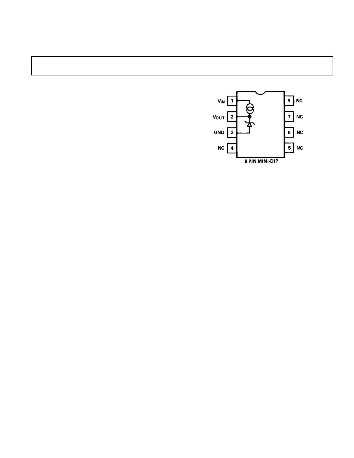
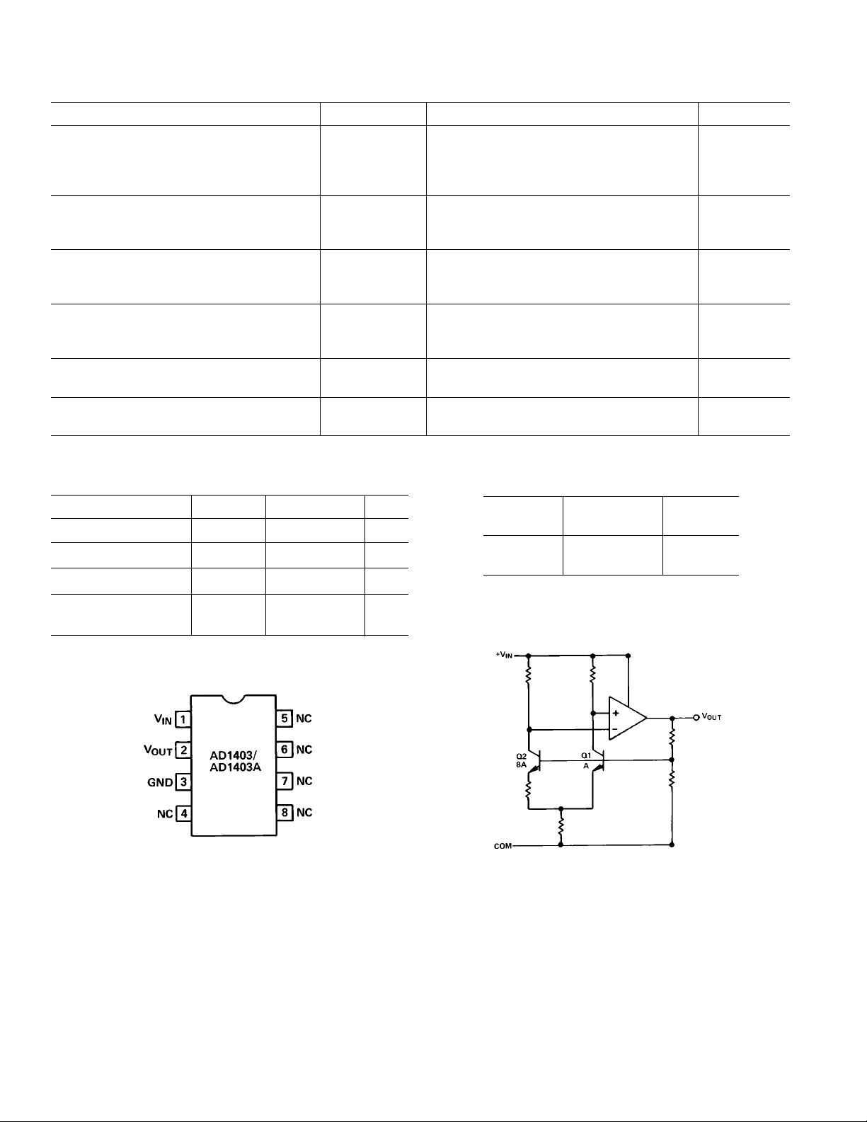
Figure 1. AD1403/AD1403A Connection Diagram
ORDERING GUIDE
Initial Package
Model Tolerance Option*
AD1403 ±25 mV N-8
AD1403A ±10 mV N-8
*N Plastic DIP.
Figure 2. Simplified AD1403 Schematic
–2–
REV. A
Page 3

Typical Performance Curves–
AD1403/AD1403A
Figure 3. Typical Change in V
(Normalized to V
@ VlN = 15 V @ TC = 25°C)
OUT
OUT
vs. V
IN
Figure 4. Change in Output Voltage vs. Load Current
(Normalized to V
@ VIN = 15 V, l
OUT
= 0 mA)
OUT
Figure 5. Quiescent Current vs. Temperature
(V
= 15 V, I
IN
= 0 mA)
OUT
Figure 6. Change in V
(Normalized to V
OUT
Figure 7. Change in V
(Normalized to V
@ VlN = 15 V, I
OUT
vs. Temperature
OUT
@ VIN = 15 V)
vs. Temperature
OUT
= 0 mA)
OUT
VOLTAGE VARIATION VS. TEMPERATURE AND LINE
Some confusion exists in the area of defining and specifying reference voltage error over temperature. Historically, references
are characterized using a maximum deviation per degree Centigrade; i.e., 10 ppm/°C. However, because of the inconsistent
nonlinearities in Zener references (butterfly or “S” type characteristics), most manufacturers use a maximum limit error band
approach to characterize their references. This technique measures the output voltage at 3 to 5 different temperatures and
guarantees that the output voltage deviation will fall within the
guaranteed error band at these discrete temperatures. This approach, of course, makes no mention or guarantee of performance at any other temperature within the operating
temperature range of the device.
The consistent Voltage vs. Temperature performance of a typical AD1403 is shown in Figure 6. Note that the characteristic is
quasi-parabolic, not the possible “S” type characteristics of classical Zener references. This parabolic characteristic permits a
maximum output deviation specification over the device’s full
operating temperature range, rather than just at 3 to 5 discrete
temperatures.
REV. A
–3–
Page 4

Applying the AD1403/AD1403A
AD1403/AD1403A
The AD1403 exhibits a worst-case shift of 7.5 mV over the entire range of operating input voltage, 4.5 volts to 40 volts. Typically, the shift is less than 1 mV as shown in Figure 3.
THE AD1403A AS A LOW POWER, LOW VOLTAGE PRECISION REFERENCE FOR DATA CONVERTERS
The AD1403A has a number of features that make it ideally
suited for use with A/D and D/A data converters used in complex microprocessor-based systems. The calibrated 2.500 volt
output minimizes user trim requirements and allows operation
from a single low voltage supply. Low power consumption
(1.5 mA quiescent current) is commensurate with that of CMOStype devices, while the low cost and small package complements
the decreasing cost and size of the latest converters.
Figure 8 shows the AD1403A used as a reference for the
AD7524 low-cost 8-bit CMOS DAC with complete micro-
Figure 9a shows the AD1403 connected as a current source.
Total current is equal to the quiescent current plus the load
current. Most of the temperature coefficient comes from the
quiescent current term I
(1300 ppm/°C). The load voltage (and hence current) TC is
much lower at ±40 ppm/°C max (AD1403). Therefore, the
overall temperature coefficient decreases rapidly as the load current is increased. Figure 9b shows the typical temperature coefficient for currents between 1.5 mA and 10 mA. Use of an
AD1403A will not improve the TC appreciably.
Figure 9a. The AD1403 as a Precision Programmable
Current Source
, which has a typical TC of 0.13%/°C
I
C551a–9–7/82
Figure 8. Low Power, Low Voltage Reference for the
AD7524 Microprocessor-Compatible 8-Bit DAC
processor interface. The AD1403A and the AD7524 are specified to operate from a single 5 volt supply; this eliminates the
need to provide a +15 volt power supply for the sole purpose of
operating a reference. The AD7524 includes an 8-bit data register, and address decoding logic; it may thus be interfaced directly to an 8- or 16-bit data bus. Only 300 µA of quiescent
current from the single +5 volt supply is required to operate the
AD7524 which is packaged in a small 16-pin DIP. The AD542
output amplifier is also low power, requiring only 1.5 mA quiescent current. Its laser-trimmed offset voltage preserves the ± 1/2
LSB linearity of the AD7524KN without user trims and it typically settles to ±1/2 LSB in less than 5 microseconds. It will provide the 0 volt to –2.5 volt output swing from ± 5 volt supplies.
THE AD1403 AS A PRECISION PROGRAMMABLE CURRENT SOURCE
The AD1403 is an excellent building block for precision current
sources. Its wide range of operating voltages, 4.5 V to 40 V,
along with excellent line regulation over that range (7.5 mV)
result in high insensitivity to varying load impedances. The low
quiescent current (I
fied maximum load current of 10 mA allows the user to program current to any value between 1.5 mA and 10 mA.
) of 1.5 mA (max) and the maximum speci-
I
–4–
Figure 9b. Typical Temperature Coefficient of Current
Source
OUTLINE DIMENSIONS
Dimensions shown in inches and (mm).
8-Pin Mini-DIP (N)
PRINTED IN U.S.A.
REV. A
 Loading...