

Page 1
Dual-Channel, 12-Bit, 80 MSPS ADC
A
FEATURES
Dual 80 MSPS, minimum sample rate
Channel-to-channel matching, ±1% gain error
90 dB channel-to-channel isolation
DC-coupled signal conditioning
80 dB spurious-free dynamic range
Selectable bipolar inputs (±1 V and ±0.5 V ranges)
Integral single-pole, low-pass Nyquist filter
Twos complement output format
3.3 V compatible outputs
1.85 W per channel
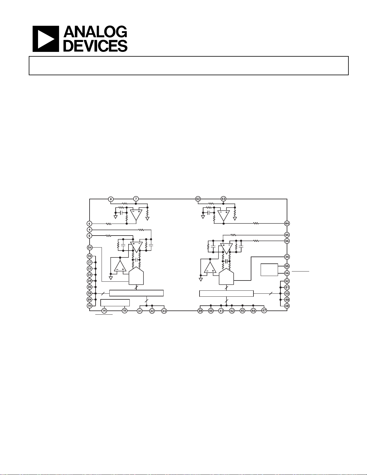
FUNCTIONAL BLOCK DIAGRAM
AMP-IN-A-1
VREF
DROUT
100Ω OUTPUT TERMINATORS
TIMING
12
AMP-OUT-A
A–IN
A+IN
DROUTA
D0A (LSB)
D1A
D2A
D3A
D4A
D5A
D6A
D7A
D8A
AMP-IN-A-2
9
with Analog Input Signal
Conditioning
AD13280
APPLICATIONS
Radar processing (optimized for I/Q baseband operation)
Phased array receivers
Multichannel, multimode receivers
GPS antijamming receivers
Communications receivers
PRODUCT HIGHLIGHTS
1. Guaranteed sample rate of 80 MSPS.
2. Input signal conditioning; gain and impedance match.
3. Single-ended, differential, or off-module filter option.
4. Fully tested/characterized full channel performance.
MP-IN-B-2AMP-IN-B-1
AMP-OUT-B
B+IN
AD13280
TIMING
VREF
DROUT
12
100Ω OUTPUT TERMINATORS
3
7
5
B–IN
DROUTB
ENCODEB
ENCODEB
D11B (MSB)
D10B
D9B
D8B
D7B
ENCODEAENCODEA
D9A D10A D11A
(MSB)
D0B
D1B D3BD2B D4B D5B D6B
(LSB)
02386-001
Figure 1.
Rev. C
Information furnished by Analog Devices is believed to be accurate and reliable. However, no
responsibility is assumed by Anal og Devices for its use, nor for any infringements of patents or ot her
rights of third parties that may result from its use. Specifications subject to change without notice. No
license is granted by implication or otherwise under any patent or patent rights of Analog Devices.
Trademarks and registered trademarks are the property of their respective owners.
One Technology Way, P.O. Box 9106, Norwood, MA 02062-9106, U.S.A.
Tel: 781.329.4700 www.analog.com
Fax: 781.461.3113 ©2002–2008 Analog Devices, Inc. All rights reserved.
Page 2

AD13280
TABLE OF CONTENTS
Features.............................................................................................. 1
Applications....................................................................................... 1
Product Highlights ........................................................................... 1
Functional Block Diagram .............................................................. 1
Revision History ............................................................................... 2
General Description ......................................................................... 3
Specifications..................................................................................... 4
Timing Diagram........................................................................... 6
Absolute Maximum Ratings............................................................ 7
Explanation of Test Levels........................................................... 7
ESD Caution.................................................................................. 7
Pin Configuration and Function Descriptions............................. 8
Typical Performance Characteristics ........................................... 10
Terminology .................................................................................... 12
Input and Output Stages................................................................ 13
Theory of Operation ...................................................................... 14
Using the Single-Ended Input .................................................. 14
Using the Differential Input...................................................... 14
Applications Information.............................................................. 15
Encoding the AD13280 ............................................................. 15
Jitter Consideration.................................................................... 15
Power Supplies............................................................................ 16
Output Loading .......................................................................... 16
Evaluation Board............................................................................ 17
Layout Information.................................................................... 17
Bill of Materials List for Evaluation Board.............................. 24
Outline Dimensions....................................................................... 25
Ordering Guide .......................................................................... 26
REVISION HISTORY
4/08—Rev. B to Rev. C
Updated Outline Dimensions....................................................... 25
Changes to the Ordering Guide.................................................... 26
11/05—Rev. A to Rev. B
Updated Format..................................................................Universal
Changes to Features and Product Highlights ............................... 1
Changes to General Description .................................................... 3
Changes to Table 1............................................................................ 4
Changes to Figure 3.......................................................................... 8
Changes to Theory of Operation.................................................. 14
Changes to Equation 1................................................................... 15
Changes to Table 5.......................................................................... 18
Changes to Figure 21...................................................................... 19
Changes to Figure 22...................................................................... 20
Changes to Figure 23...................................................................... 21
Changes to Figure 28 and Figure 29............................................. 24
Updated Outline Dimensions....................................................... 25
Changes to the Ordering Guide.................................................... 26
8/02—Rev. 0 to Rev. A
Edits to Specifications.......................................................................2
Packages Updated........................................................................... 19
Rev. C | Page 2 of 28
Page 3

AD13280
GENERAL DESCRIPTION
The AD13280 is a complete, dual-channel, signal processing
solution that includes on-board amplifiers, references, ADCs, and
output termination components to provide optimized system
performance. The AD13280 has on-chip track-and-hold circuitry
and uses an innovative multipass architecture to achieve 12-bit, 80
MSPS performance. The AD13280 uses innovative high density
circuit design and laser-trimmed thin-film resistor networks to
achieve exceptional channel matching, impedance control, and
performance while maintaining excellent isolation and
providing for significant board area savings.
Multiple options are provided for driving the analog input,
including single-ended, differential, and optional series filtering. The AD13280 also offers users a choice of analog input
signal ranges to further minimize additional external signal
conditioning, while remaining general purpose.
The AD13280 operates with ±5.0 V for the analog signal conditioning with a separate 5.0 V supply for the analog-to-digital
conversion and 3.3 V digital supply for the output stage. Each
channel is completely independent, allowing operation with
independent encode and analog inputs and maintaining
minimal crosstalk and interference.
The AD13280 is available in a 68-lead, ceramic gull wing package.
The components are manufactured using the Analog Devices, Inc.,
high speed complementary bipolar process (XFCB).
Rev. C | Page 3 of 28
Page 4

AD13280
SPECIFICATIONS
AVCC = +5 V, AVEE = −5 V, DVCC = +3.3 V; applies to each ADC with front-end amplifier, unless otherwise noted.
Table 1.
AD13280AZ
Parameter Temperature Test Level Min Typ Max Unit
RESOLUTION 12 Bits
DC ACCURACY
No Missing Codes Full IV Guaranteed
Offset Error 25°C I −2.2 ±1.0 +2.2 % FS
Full VI −2.2 ±1.0 +2.2 % FS
Offset Error Channel Match Full VI −1.0 ±0.1 +1.0 %
Gain Error
Full VI −5.0 ±2.0 +5.0 % FS
Gain Error Channel Match 25°C I −1.5 ±0.5 +1.5 %
Max VI −3.0 ±1.0 +3.0 %
Min VI −5 ±1.0 +5 %
SINGLE-ENDED ANALOG INPUT
Input Voltage Range
AMP-IN-X-1 Full V ±0.5 V
AMP-IN-X-2 Full V ±1.0 V
Input Resistance
AMP-IN-X-1 Full IV 99 100 101 Ω
AMP-IN-X-2 Full IV 198 200 202 Ω
Capacitance 25°C V 4.0 7.0 pF
Analog Input Bandwidth
DIFFERENTIAL ANALOG INPUT
Analog Signal Input Range
A+IN to A–IN and B+IN to B−IN
Input Impedance 25°C V 618 Ω
Analog Input Bandwidth Full V 50 MHz
ENCODE INPUT (ENCODE, ENCODE)
Differential Input Voltage Full IV 0.4 V p-p
Differential Input Resistance 25°C V 10 kΩ
Differential Input Capacitance 25°C V 2.5 pF
SWITCHING PERFORMANCE
Maximum Conversion Rate
Minimum Conversion Rate
Aperture Delay (tA) 25°C V 0.9 ns
Aperture Delay Matching 25°C IV 250 500 ps
Aperture Uncertainty (Jitter) 25°C V 0.3 ps rms
ENCODE Pulse Width High at Max Conversion Rate 25°C IV 4.75 6.25 8 ns
ENCODE Pulse Width Low at Max Conversion Rate 25°C IV 4.75 6.25 8 ns
Output Delay (tOD) Full V 5 ns
Encode, Rising to Data Ready, Rising Delay Full V 8.5 ns
1, 6
SNR
Analog Input @ 10 MHz 25°C I 66.5 70 dBFS
Min II 64.5 dBFS
Max II 66.3 dBFS
Analog Input @ 21 MHz 25°C I 66.5 70 dBFS
Min II 64 dBFS
Max II 66.3 dBFS
1
2
3
4
1
5
5
25°C I −3 −1.0 +1 % FS
Full V 143 MHz
Full V ±1 V
Full VI 80 MSPS
Full IV 30 MSPS
Rev. C | Page 4 of 28
Page 5

AD13280
AD13280AZ
Parameter Temperature Test Level Min Typ Max Unit
Analog Input @ 37 MHz 25°C I 63 65 dBFS
Min II 61.5 dBFS
Max II 63 dBFS
1, 7
SINAD
Min II 53 dBFS
Max II 54 dBFS
SPURIOUS-FREE DYNAMIC RANGE
Min II 55
Max II 55
SINGLE-ENDED ANALOG INPUT
DIFFERENTIAL ANALOG INPUT
TWO-TONE IMD REJECTION9
CHANNEL-TO-CHANNEL ISOLATION10 25°C IV 90 dB
TRANSIENT RESPONSE 25°C V 25 ns
DIGITAL OUTPUTS11
POWER SUPPLY
Analog Input @ 10 MHz 25°C I 66 69 dBFS
Min II 63.5 dBFS
Max II 66 dBFS
Analog Input @ 21 MHz 25°C I 64 68.5 dBFS
Min II 63 dBFS
Max II 64 dBFS
Analog Input @ 37 MHz 25°C I 54 59 dBFS
1, 8
Analog Input @ 10 MHz 25°C I 75 80 dBFS
Min II 70
Max II 75
Analog Input @ 21 MHz 25°C I 68 75 dBFS
Min II 67
Max II 67
Analog Input @ 37 MHz 25°C I 56 62 dBFS
Pass-Band Ripple to 10 MHz 25°C V 0.07 dB
Pass-Band Ripple to 25 MHz 25°C V 0.12 dB
Pass-Band Ripple to 10 MHz 25°C V 0.3 dB
Pass-Band Ripple to 25 MHz 25°C V 0.82 dB
fIN = 9.1 MHz and 10.1 MHz (f1 and f2 are −7 dBFS) 25°C I 75 80 dBc
Min II 71
Max II 74
fIN = 19.1 MHz and 20.7 MHz (f1 and f2 are −7 dBFS) 25°C V 77 dBc
fIN = 36 MHz and 37 MHz (f1 and f2 are −7 dBFS) 25°C V 60 dBc
Logic Compatibility CMOS
DVCC = 3.3 V
Logic 1 Voltage Full I 2.5 DVCC − 0.2 V
Logic 0 Voltage Full I 0.2 0.5 V
DVCC = 5 V
Logic 1 Voltage Full V DVCC − 0.3 V
Logic 0 Voltage Full V 0.35 V
Output Coding Twos complement
AVCC Supply Voltage12 Full IV 4.85 5.0 5.25 V
I (AVCC) Current Full I 313 364 mA
AVEE Supply Voltage12 Full IV −5.25 −5.0 −4.75 V
I (AVEE) Current Full I 38 49 mA
DVCC Supply Voltage12 Full IV 3.135 3.3 3.465 V
Rev. C | Page 5 of 28
Page 6
AD13280
AD13280AZ
Parameter Temperature Test Level Min Typ Max Unit
I (DVCC) Current Full I 34 46 mA
ICC (Total) Supply Current per Channel Full I 375 459 mA
Power Dissipation (Total) Full I 3.7 4.3 W
Power Supply Rejection Ratio (PSRR) Full V 0.01 % FSR/% VS
1
All ac specifications tested by driving ENCODE and
2
Gain tests are performed on the AMP-IN-x-1 input voltage range.
3
Full power bandwidth is the frequency at which the spectral power of the fundamental frequency (as determined by FFT analysis) is reduced by 3 dB.
4
For differential input: +IN = 1 V p-p and −IN = 1 V p-p (signals are 180 Ω out of phase). For single-ended input: +IN = 2 V p-p and –IN = GND.
5
Minimum and maximum conversion rates allow for variation in encode duty cycle of 50% ± 5%.
6
Analog input signal power at –1 dBFS; signal-to-noise ratio (SNR) is the ratio of signal level to total noise (first five harmonics removed). Encode = 80 MSPS. SNR is
reported in dBFS, related back to converter full scale.
7
Analog input signal power at –1 dBFS; signal-to-noise and distortion (SINAD) is the ratio of signal level to total noise + harmonics. Encode = 80 MSPS. SINAD is
reported in dBFS, related back to converter full scale.
8
Analog input signal at –1 dBFS; SFDR is the ratio of converter full scale to worst spur.
9
Both input tones at –7 dBFS; two-tone intermodulation distortion (IMD) rejection is the ratio of either tone to the worst third-order intermodulation product.
10
Channel-to-channel isolation tested with A channel grounded and a full-scale signal applied to B channel.
11
Digital output logic levels: DVCC = 3.3 V, C
12
Supply voltage recommended operating range. AVCC may be varied from 4.85 V to 5.25 V. However, rated ac (harmonics) performance is valid only over the range
AVCC = 5.0 V to 5.25 V.
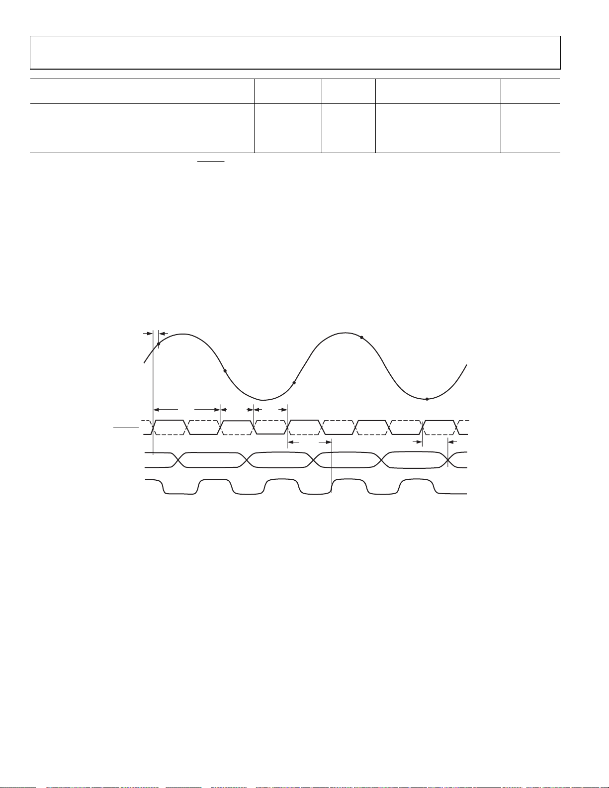
TIMING DIAGRAM
t
A
N
A
IN
ENCODE
differentially. Single-ended input: AMP-IN-x-1 = 1 V p-p, AMP-IN-x-2 = GND.
= 10 pF. Capacitive loads >10 pF degrades performance.
LOAD
N + 1
N + 2
N + 3
ENCODE,
ENCODE
D[11:0]
DRY
t
ENC
N N+1 N+2 N+3 N + 4
t
ENCH
N – 3 N – 2 N – 1
t
ENCL
t
E_DR
N + 4
t
OD
N
Figure 2.
2386-012
Rev. C | Page 6 of 28
Page 7
AD13280
ABSOLUTE MAXIMUM RATINGS
Table 2.
Parameter Ratings
ELECTRICAL1
AVCC Voltage 0 V to 7 V
AVEE Voltage −7 V to 0 V
DVCC Voltage 0 V to 7 V
Analog Input Voltage VEE to VCC
Analog Input Current −10 mA to +10 mA
Digital Input Voltage (ENCODE) 0 to VCC
ENCODE, ENCODE Differential Voltage
Digital Output Current −10 mA to +10 mA
ENVIRONMENTAL1
Operating Temperature Range (Case) −40°C to +85°C
Maximum Junction Temperature 175°C
Lead Temperature (Soldering, 10 sec) 300°C
Storage Temperature Range (Ambient) −65°C to +150°C
1
Typical thermal impedance for ES package: θJC 2.2°C/W; θJA 24.3°C/W.
4 V max
Stresses above those listed under Absolute Maximum Ratings
EXPLANATION OF TEST LEVELS
I. 100% production tested.
II. 100% production tested at 25°C, and sample tested
at specified temperatures. AC testing done on a
sample basis.
III. Sample tested only.
IV. Parameter guaranteed by design and characterization
testing.
V. Parameter is a typical value only.
VI. 100% production tested with temperature at 25°C, and
sample tested at temperature extremes.
ESD CAUTION
may cause permanent damage to the device. This is a stress
rating only; functional operation of the device at these or any
other conditions above those indicated in the operational
section of this specification is not implied. Exposure to absolute
maximum rating conditions for extended periods may affect
device reliability.
Rev. C | Page 7 of 28
Page 8
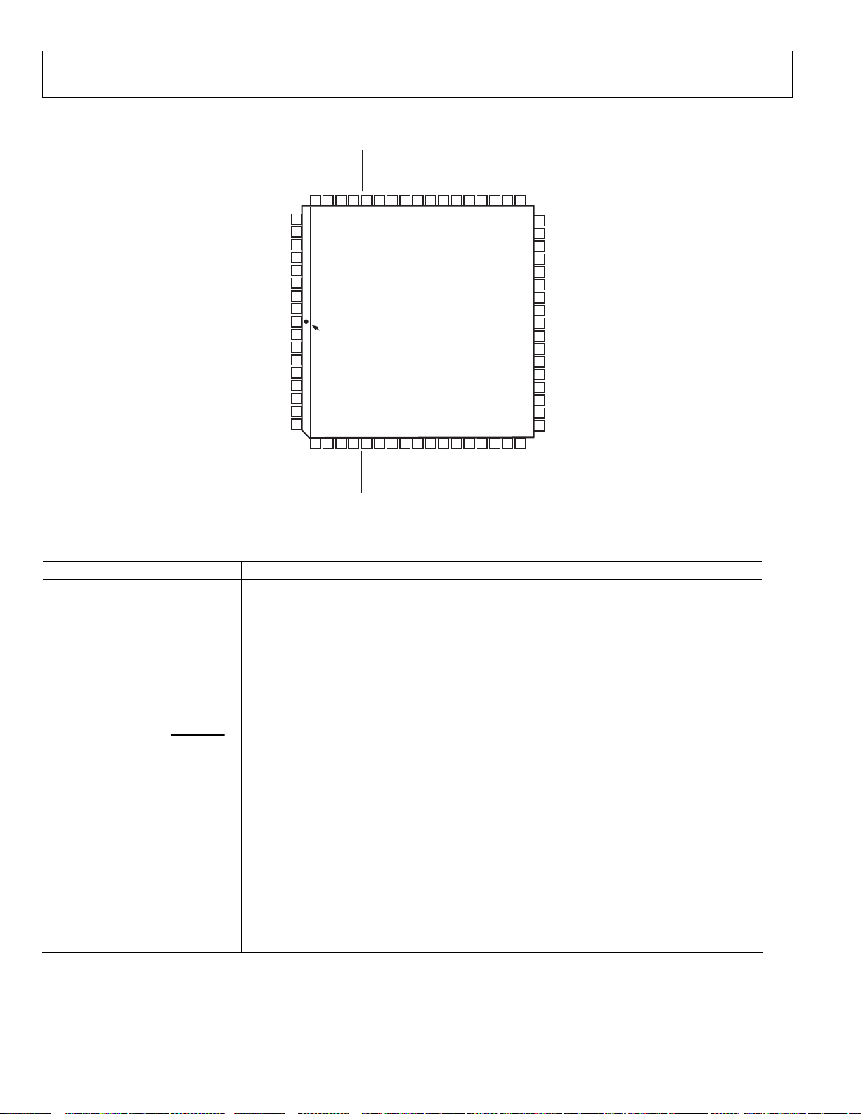
AD13280
A
PIN CONFIGURATION AND FUNCTION DESCRIPTIONS
B
CC
D11B (MSB)
AGNDB
DV
AD13280
TOP VIEW
A
NC
CC
DV
AGNDA
D10B
ENCODEB
ENCODEB
(Not to Scale)
ENCODEA
ENCODEA
NC = NO CONNECT
NC
D9B
D0A (LSB)
D8B
D1A
D7B
D2A
D6B
D3A
D5B
D4A
D4B
D5A
444546474849505160 59 58 57 56 55 54 53 52
DGNDB
DGNDA
43
DGNDB
42
D3B
41
D2B
40
D1B
39
D0B (LSB)
NC
38
37
NC
36
DROUTB
35
SHIELD
34
DROUTA
33
D11A (MSB)
32
D10A
31
D9A
30
D8A
29
D7A
28
D6A
27
DGNDA
02386-002
AGNDB
AMP-IN-B-2
AMP-IN-B-1
MP-OUT-B
B+IN
B–IN
AGNDB
AGNDB
SHIELD
AGNDA
AGNDA
A–IN
A+IN
AMP-OUT-A
AMP-IN-A-1
AMP-IN-A-2
AGNDA
B
B
EE
CC
AGNDB
AV
AGNDB
AV
61
62
63
64
65
66
67
68
1
PIN 1
2
IDENTIFIER
3
4
5
6
7
8
9
10 2611 12 13 14 15 16 17 18 19 20 21 22 23 24 25
A
A
EE
CC
AV
AV
AGNDA
AGNDA
Figure 3. Pin Configuration
Table 3. Pin Function Descriptions
Pin No. Mnemonic Description
1, 35 SHIELD Internal Ground Shield Between Channels.
2, 3, 9, 10, 13, 16 AGNDA A Channel Analog Ground. A and B grounds should be connected as close to the device as possible.
4 A−IN Inverting Differential Input (Gain = +1).
5 A+IN Noninverting Differential Input (Gain = +1).
6 AMP-OUT-A Single-Ended Amplifier Output (Gain = +2).
7 AMP-IN-A-1 Analog Input for A Side ADC (Nominally ±0.5 V ).
8 AMP-IN-A-2 Analog Input for A Side ADC (Nominally ±1.0 V ).
11 AVEEA A Channel Analog Negative Supply Voltage (Nominally −5.0 V or −5.2 V).
12 AVCCA A Channel Analog Positive Supply Voltage (Nominally +5.0 V).
14
ENCODEA
Complement of ENCODEA. Differential input.
15 ENCODEA Encode Input. Conversion initiated on rising edge.
17 DVCCA A Channel Digital Positive Supply Voltage (Nominally +5.0 V/+3.3 V).
18, 19, 37, 38 NC No Connect.
20 to 25, 28 to 33
D0A to
Digital Outputs for ADC A. D0 (LSB).
D11A
26, 27 DGNDA A Channel Digital Ground.
34 DROUTA Data Ready A Output.
36 DROUTB Data Ready B Output.
39 to 42, 45 to 52
D0B to
Digital Outputs for ADC B. D0 (LSB).
D11B
43, 44 DGNDB B Channel Digital Ground.
53 DVCCB B Channel Digital Positive Supply Voltage (Nominally +5.0 V/+3.3 V).
Rev. C | Page 8 of 28
Page 9

AD13280
Pin No. Mnemonic Description
54, 57, 60, 61, 67, 68 AGNDB B Channel Analog Ground. A and B grounds should be connected as close to the device as possible.
55 ENCODEB Encode Input. Conversion initiated on rising edge.
56
58 AVCCB B Channel Analog Positive Supply Voltage (Nominally +5.0 V).
59 AVEEB B Channel Analog Negative Supply Voltage (Nominally −5.0 V or −5.2 V).
62 AMP-IN-B-2 Analog Input for B Side ADC (Nominally ±1.0 V).
63 AMP-IN-B-1 Analog Input for B Side ADC (Nominally ±0.5 V).
64 AMP-OUT-B Single-Ended Amplifier Output (Gain = +2).
65 B+IN Noninverting Differential Input (Gain = +1).
66 B−IN Inverting Differential Input (Gain = +1).
ENCODEB
Complement of ENCODEB. Differential input.
Rev. C | Page 9 of 28
Page 10

AD13280
TYPICAL PERFORMANCE CHARACTERISTICS
dB
dB
dB
–10
–20
–30
–40
–50
–60
–70
–80
–90
–100
–110
–120
–130
–10
–20
–30
–40
–50
–60
–70
–80
–90
–100
–110
–120
–130
–10
–20
–30
–40
–50
–60
–70
–80
–90
–100
–110
–120
–130
0
3
2
0
51015 302520
FREQUENCY (MHz )
Figure 4. Single Tone @ 5 MHz
0
0
51015 302520
FREQUENCY (MHz)
Figure 5. Single Tone @ 18 MHz
0
0
51015 302520
FREQUENCY (MHz )
Figure 6. Two Tone @ 9 MHz and 10 MHz
4
ENCODE = 80MSPS
= 5MHz (–1dBFS)
A
IN
SNR = 69.4dBFS
SFDR = 81.9dBc
5
6
35 40
ENCODE = 80MSPS
A
= 18MHz (–1dBFS)
IN
SNR = 69.79dBF S
SFDR = 76.81dBc
35 40
ENCODE = 80MSPS
A
= 9MHz AND
IN
10MHz (–7dBFS)
SFDR = 82.77dBc
35 40
02386-003
02386-004
02386-005
dB
dB
dB
–10
–20
–30
–40
–50
–60
–70
–80
–90
–100
–110
–120
–130
–10
–20
–30
–40
–50
–60
–70
–80
–90
–100
–110
–120
–130
–10
–20
–30
–40
–50
–60
–70
–80
–90
–100
–110
–120
–130
0
0
0
0
0
0
ENCODE = 80MSPS
= 10MHz (–1dBFS)
A
IN
SNR = 69.19dBF S
SFDR = 79.55dBc
2
6
51015 302520
FREQUENCY (MHz)
5
Figure 7. Single Tone @ 10 MHz
ENCODE = 80MSPS
A
= 37MHz (–1dBF S)
IN
SNR = 68.38dBFS
SFDR = 57.81dBc
2
6
4
51015 302520
FREQUENCY (MHz)
5
Figure 8. Single Tone @ 37 MHz
ENCODE = 80MSPS
A
= 19MHz AND
IN
20MHz (–7dBF S)
SFDR = 74.41dBc
51015 302520
FREQUENCY (MHz)
Figure 9. Two Tone @ 19 MHz and 20 MHz
3
4
35 40
02386-006
3
35 40
02386-007
35 40
02386-008
Rev. C | Page 10 of 28
Page 11

AD13280
3.0
2.5
2.0
1.5
ENCODE = 80MSPS
DNL MAX = 0. 688 CODES
DNL MIN = 0. 385 CODES
3
ENCODE = 80MSPS
2
1
INL MAX = 0. 562 CODES
INL MIN = 0. 703 CODES
LSB
–0.5
–1.0
dBFS
–10
1.0
0.5
0
0
–1
–2
–3
–4
–5
–6
–7
–8
–9
1.0 3.5
0 512
1024 1536 2048 2560 3072 3584 4096
Figure 10. Differential Nonlinearity
ENCODE = 80MSPS
ROLL-O FF = 0. 0459dB
6.0 8. 5 11.0 13.5 16.0 18.5 2 1.0 23.5 26.0
FREQUENCY ( MHz)
Figure 11. Pass-Band Ripple to 25 MHz
0
LSB
–1
–2
–3
512 1024 1536 2048 2560 3072 3584 4096
02386-009
0
02386-011
Figure 12. Integral Nonlinearity
02386-010
Rev. C | Page 11 of 28
Page 12

AD13280
TERMINOLOGY
Analog Bandwidth
The analog input frequency at which the spectral power of the
fundamental frequency (as determined by the FFT analysis) is
reduced by 3 dB.
Aperture Delay
The delay between a differential crossing of the ENCODEA
signal and the
analog input is sampled.
Aperture Uncertainty (Jitter)
The sample-to-sample variation in aperture delay.
Differential Analog Input Resistance, Differential Analog
Input Capacitance, and Differential Analog Input Impedance
The real and complex impedances measured at each analog
input port. The resistance is measured statically, and the
capacitance and differential input impedances are measured
with a network analyzer.
Differential Analog Input Voltage Range
The peak-to-peak differential voltage that must be applied to
the converter to generate a full-scale response. Peak differential
voltage is computed by observing the voltage from the other
pin, which is 180 degrees out of phase. Peak-to-peak differential
is computed by rotating the input phase 180 degrees and taking
the peak measurement again. The difference is then computed
between both peak measurements.
Differential Nonlinearity
The deviation of any code from an ideal 1 LSB step.
ENCODE Pulse Width/Duty Cycle
Pulse width high is the minimum amount of time that the
ENCODE pulse should be left in a Logic 1 state to achieve the
rated performance. Pulse width low is the minimum time the
ENCODE pulse should be left in a low state. At a given clock
rate, these specifications define an acceptable encode duty cycle.
Harmonic Distortion
The ratio of the rms signal amplitude to the rms value of the
worst harmonic component.
Integral Nonlinearity
The deviation of the transfer function from a reference line
measured in fractions of 1 LSB using a best straight line
determined by a least square curve fit.
ENCODEA
signal and the instant at which the
Minimum Conversion Rate
The encode rate at which the SNR of the lowest analog signal
frequency drops by no more than 3 dB below the guaranteed
limit.
Maximum Conversion Rate
The encode rate at which parametric testing is performed.
Output Propagation Delay
The delay between a differential crossing of the ENCODEA
signal and the
output data bits are within valid logic levels.
Overvoltage Recovery Time
The amount of time required for the converter to recover to
0.02% accuracy after an analog input signal of the specified
percentage of full scale is reduced to midscale.
Power Supply Rejection Ratio
The ratio of a change in input offset voltage to a change in
power supply voltage.
Signal-to-Noise-and-Distortion (SINAD)
The ratio of the rms signal amplitude (set at 1 dB below full
scale) to the rms value of the sum of all other spectral components, including harmonics but excluding dc. SINAD can be
reported in dB (that is, degrades as signal level is lowered) or
in dBFS (always related back to converter full scale).
Signal-to-Noise Ratio (SNR) (Without Harmonics)
The ratio of the rms signal amplitude (set at 1 dB below full
scale) to the rms value of the sum of all other spectral components, excluding the first five harmonics and dc. SNR can be
reported in dB (that is, degrades as signal level is lowered) or
in dBFS (always related back to converter full scale).
Spurious-Free Dynamic Range (SFDR)
The ratio of the rms signal amplitude to the rms value of
the peak spurious spectral component. The peak spurious
component may or may not be a harmonic.
Transi ent Res p ons e
The time required for the converter to achieve 0.02% accuracy
when a one-half full-scale step function is applied to the analog
input.
Two-Tone Intermodulation Distortion Rejection
The ratio of the rms value of either input tone to the rms value
of the worst third-order intermodulation product; reported in
dBc.
ENCODEA
signal and the time at which all
Rev. C | Page 12 of 28
Page 13

AD13280
A
A
INPUT AND OUTPUT STAGES
LOADS
AV
AV
AV
CC
CC
AV
CC
CC
MP-IN-X-2
MP-IN-X-1
100
100Ω
Ω
TOAD8045
Figure 13. Single-Ended Input Stage
DV
CC
CURRENT MIRROR
DV
V
REF
10kΩ
ENCODE
10kΩ
2386-013
LOADS
10kΩ
10k
ENCODE
Ω
02386-014
Figure 15. ENCODE Inputs
DV
CC
CURRENT MIRROR
CC
DROUT
DV
CC
V
REF
100Ω
D0–D11
CURRENT MIRROR
02386-015
Figure 14. DR Digital Output Stage
CURRENT MIRROR
Figure 16. Digital Output Stage
2386-016
Rev. C | Page 13 of 28
Page 14

AD13280
THEORY OF OPERATION
The AD13280 is a high dynamic range 12-bit, 80 MHz pipeline
delay (three pipelines) analog-to-digital converter (ADC). The
custom analog input section provides input ranges of 1 V p-p
and 2 V p-p and input impedance configurations of 50 Ω, 100 Ω,
and 200 Ω.
The AD13280 employs four monolithic Analog Devices components per channel (
ADC IC), along with multiple passive resistor networks and
decoupling capacitors to fully integrate a complete 12-bit
analog-to-digital converter (ADC).
In the single-ended input configuration, the input signal is passed
through a precision laser-trimmed resistor divider, allowing the
user to externally select operation with a full-scale signal of ±0.5 V
or ±1.0 V by choosing the proper input terminal for the application. The result of the resistor divider is to apply a full-scale
input of approximately 0.4 V to the noninverting input of the
internal
The AD13280 analog input includes an
featuring an innovative architecture that maximizes the dynamic
range capability on the amplifier inputs and outputs. The
amplifier provides a high input impedance and gain for driving the
AD8138 in a single-ended to differential amplifier configuration.
The
differential signal with the lowest harmonic distortion available in
a differential amplifier. The
balance the differential inputs to the custom ADC, maximizing
the performance of the device.
The
analog-to-digital converter. The internal reference voltage of
the custom ADC is designed to track the offsets and drifts and
is used to ensure matching over an extended temperature range
of operation. The reference voltage is connected to the output
common-mode input on the
sets the output common mode on the
is the midsupply level for the ADC.
The custom ADC has complementary analog input pins,
and AIN. Each analog input is centered at 2.4 V and should
swing ±0.55 V around this reference. Because AIN and
180 degrees out of phase, the differential analog input signal is
2.2 V peak-to-peak. Both analog inputs are buffered prior to
the first track-and-hold.
The custom ADC digital outputs drive 100 Ω series resistors
(see
compatible word, coded as a twos complement.
AD8045 amplifier.
AD8138 has a −3 dB bandwidth at 300 MHz and delivers a
AD8031 provides the buffer for the internal reference
Figure 16). The result is a 12-bit, parallel digital CMOS-
AD8045, AD8138, AD8031, and a custom
AD8045 amplifier
AD8045
AD8138 differential outputs help
AD8138. This reference voltage
AD8138 at 2.4 V, which
AIN
AIN
are
USING THE SINGLE-ENDED INPUT
The AD13280 has been designed with user ease of operation in
mind. Multiple input configurations have been included onboard to allow the user a choice of input signal levels and input
impedance. The standard inputs are ±0.5 V and ±1.0 V. The
user can select the input impedance of the AD13280 on any
input by using the other inputs as alternate locations for the
GND. The following is a summary of the impedance options
available at each input location:
AMP-IN-x-1 = 100 Ω when AMP-IN-x-2 is open.
AMP-IN-x-1 = 50 Ω when AMP-IN-x-2 is shorted to GND.
AMP-IN-x-2 = 200 Ω when AMP-IN-x-1 is open.
Each channel has two analog inputs: AMP-IN-A-1 and
AMP-IN-A-2 or AMP-IN-B-1 and AMP-IN-B-2. Use
AMP-IN-A-1 or AMP-IN-B-1 when an input of ±0.5 V full
scale is desired. Use AMP-IN-A-2 or AMP-IN-B-2 when ±1 V
full scale is desired. Each channel has an AMP-OUT that must
be tied to either a noninverting or inverting input of a
differential amplifier with the remaining input grounded. For
example, Side A, AMP-OUT-A (Pin 6) must be tied to A+IN
(Pin 5) with A−IN (Pin 4) tied to ground for noninverting
operation or AMP-OUT-A (Pin 6) tied to A−IN (Pin 4) with
A+IN (Pin 5) tied to ground for inverting operation.
USING THE DIFFERENTIAL INPUT
Each channel of the AD13280 is designed with two optional
differential inputs, A+IN, A−IN and B+IN, B−IN. The inputs
provide system designers with the ability to bypass the
amplifier and drive the
tial ADC driver can be deployed in either a single-ended or
differential input configuration. The differential analog inputs
have a nominal input impedance of 620 Ω and nominal fullscale input range of 1.2 V p-p. The
differential filter and the custom analog-to-digital converter.
The differential input configuration provides the lowest evenorder harmonics and signal-to-noise (SNR) performance
improvement of up to 3 dB (SNR = 73 dBFS). Exceptional care
was taken in the layout of the differential input signal paths.
The differential input transmission line characteristics are
matched and balanced. Equal attention to system level signal
paths must be provided in order to realize significant performance improvements.
AD8138 directly. The AD8138 differen-
AD8138 amplifier drives a
AD8045
Rev. C | Page 14 of 28
Page 15

AD13280
C
V
APPLICATIONS INFORMATION
ENCODING THE AD13280
The AD13280 encode signal must be a high quality, extremely
low phase noise source to prevent degradation of performance.
Maintaining 12-bit accuracy at 80 MSPS places a premium on
encode clock phase noise. SNR performance can easily degrade
3 dB to 4 dB with 37 MHz input signals when using a high jitter
clock source. See Analog Devices Application Note AN-501,
Aperture Uncertainty and ADC System Performance, for complete details. For optimum performance, the AD13280 must be
clocked differentially. The encode signal is usually ac-coupled
0.1µF
ENCODE
100
pins via a transformer or
T1-4T
Ω
ENCODE
AD13280
ENCODE
µF
ENCODE
T
HSMS2812
DIODES
0.1
AD13280
0.1µF
VT
ENCODE
Figure 18. Differential ECL for Encode
02386-017
02386-018
into the ENCODE and
capacitors. These pins are biased internally and require no
additional bias.
Figure 17 shows one preferred method for clocking the AD13280.
The clock source (low jitter) is converted from single-ended to
differential using an RF transformer. The back-to-back Schottky
diodes across the transformer secondary limit clock excursions
into the AD13280 to approximately 0.8 V p-p differential. This
helps prevent the large voltage swings of the clock from feeding
through to the other portions of the AD13280 and limits the
noise presented to the ENCODE inputs. A crystal clock
oscillator can also be used to drive the RF transformer if an
appropriate limited resistor (typically 100 Ω) is placed in series
with the primary.
CLOCK
SOURCE
Figure 17. Crystal Clock Oscillator—Differential Encode
If a low jitter ECL/PECL clock is available, another option is to
ac-couple a differential ECL/PECL signal to the encode input
pins as shown below. A device that offers excellent jitter performance is the MC100LVEL16 (or within the same family)
from Motorola.
L
ECL/PE
JITTER CONSIDERATION
The signal-to-noise ratio for any ADC can be predicted. When
normalized to ADC codes, Equation 1 accurately predicts the
SNR based on three terms. These are jitter, average DNL error,
and thermal noise. Each of these terms contributes to the noise
within the converter.
2
⎡
1
ε
+
⎤
⎡
⎢
log20
×−=
⎢
⎣
⎢
⎣
()
2
N
2
π
⎥
⎦
tfSNR
V
⎛
2
⎜
+×××+
rmsJANALOG
⎜
⎝
(1)
where:
f
is the analog input frequency.
ANALOG
is the rms jitter of the encode (rms sum of encode source
t
J rms
and internal encode circuitry).
ε is the average DNL of the ADC (typically 0.50 LSB).
N is the number of bits in the ADC.
V
is the analog input of the ADC (typically 5 LSB).
NOISE rms
For a 12-bit analog-to-digital converter like the AD13280,
aperture jitter can greatly affect the SNR performance as the
analog frequency is increased. The chart below shows a family
of curves that demonstrates the expected SNR performance of
the AD13280 as jitter increases. The chart is derived from
Equation 1.
For a complete discussion of aperture jitter, consult Analog
Devices Application Note AN-501, Aperture Uncertainty and
ADC System Performance.
71
70
69
68
67
66
65
64
63
SNR (–dBFS)
62
61
60
59
58
0.0
0.2
0.6
1.0
1.4
1.8
0.4
0.8
1.2
CLOCK JITT ER (ps)
2.2
1.6
2.0
Figure 19. SNR vs. Jitter
AIN = 5MHz
A
= 10MHz
IN
A
= 20MHz
IN
= 37MHz
A
IN
2.6
3.0
2.4
3.4
2.8
3.2
2
⎤
⎞
rmsNOISE
⎟
⎥
N
⎟
2
⎥
⎠
⎦
3.6
3.8
4.0
02386-019
2/1
Rev. C | Page 15 of 28
Page 16

AD13280
POWER SUPPLIES
Care should be taken when selecting a power source. Linear
supplies are strongly recommended. Switching supplies tend
to have radiated components that may be received by the
AD13280. Each of the power supply pins should be decoupled
as close as possible to the package using 0.1 μF chip capacitors.
The AD13280 has separate digital and analog power supply
pins. The analog supplies are denoted AV
supply pins are denoted DV
. AVCC and DVCC should be
CC
separate power supplies because the fast digital output swings
can couple switching current back into the analog supplies.
Note that AV
specified for DV
must be held within 5% of 5 V. The AD13280 is
CC
= 3.3 V because this is a common supply for
CC
digital ASICs.
, and the digital
CC
OUTPUT LOADING
Care must be taken when designing the data receivers for the
AD13280. The digital outputs drive an internal series resistor
(for example, 100 Ω) followed by a gate like 75LCX574. To
minimize capacitive loading, there should be only one gate on
each output pin. An example of this is shown in the evaluation
board schematic (see
AD13280 have a constant output slew rate of 1 V/ns.
A typical CMOS gate combined with a PCB trace has a load of
approximately 10 pF. Therefore, as each bit switches, 10 mA
(10 pF × 1 V ÷ 1 ns) of dynamic current per bit flows in or out
of the device. A full-scale transition can cause up to 120 mA
(12 bits × 10 mA/bit) of transient current through the output
stages. These switching currents are confined between ground
and the DVCC pin. Standard TTL gates should be avoided
because they can appreciably add to the dynamic switching
currents of the AD13280. It should also be noted that extra
capacitive loading increases output timing and invalidates
timing specifications. Digital output timing is guaranteed with
10 pF loads.
Figure 20). The digital outputs of the
Rev. C | Page 16 of 28
Page 17

AD13280
EVALUATION BOARD
The AD13280 evaluation board (see Figure 20) is designed to
provide optimal performance for evaluation of the AD13280
analog-to-digital converter. The board encompasses everything
needed to ensure the highest level of performance for evaluating
the AD13280. The board requires an analog input signal, encode
clock, and power supply inputs. The clock is buffered on-board
to provide clocks for the latches. The digital outputs and out
clocks are available at the standard 40-pin connectors J1 and J2.
Power to the analog supply pins is connected via banana jacks.
The analog supply powers the associated components and the
analog section of the AD13280. The digital outputs of the
AD13280 are powered via banana jacks with 3.3 V. Contact the
factory if additional layout or applications assistance is required.
LAYOUT INFORMATION
The schematics of the evaluation board (Figure 21, Figure 22,
Figure 23) represent a typical implementation of the
and
AD13280. The pinout of the AD13280 is very straightforward
and facilitates ease of use and the implementation of high
frequency/high resolution design practices. It is recommended
that high quality ceramic chip capacitors be used to decouple
each supply pin to ground directly at the device. All capacitors
can be standard, high quality ceramic chip capacitors.
Care should be taken when placing the digital output runs.
Because the digital outputs have such a high slew rate, the
capacitive loading on the digital outputs should be minimized.
Circuit traces for the digital outputs should be kept short and
should connect directly to the receiving gate. Internal circuitry
buffers the outputs of the ADC through a resistor network to
eliminate the need to externally isolate the device from the
receiving gate.
02386-020
Figure 20. Evaluation Board Mechanical Layout
Rev. C | Page 17 of 28
Page 18

AD13280
+5VAA
AGNDA
–5VAA
0.1µF
AGENDA
C35
0.1µF
AGNDA
OUT_3.3VDA
C36
0.1µF
DGNDA
J13
SMA
C9
0.1µF
0.1µF
AGNDA
C34
C10
J9
SMA
J3
SMA
J4
SMA
AGNDA
AGNDA
AGNDA
AGNDA
ENCODEA
ENCODEA
AGNDA
NC0A
NC1A
D0A
D1A
D2A
D3A
D4A
D5A
DGNDA
NC = NO CONNECT
E51
E69 E70
AGNDA
10
AGNDA
11
AV
EE
12
AV
CC
13
AGNDA
14
ENCODEA
15
ENCODEA
16
AGNDA
17
DV
CC
18
NC
19
NC
20
D0A(LSB)
21
D1A
22
D2A
23
D3A
24
D4A
25
D5A
26
DGNDA
AGN DA
E50
E73
E49
987654321
A
A
A
E71
E72
E74
AGNDA
AMP-IN-A-2
A+IN
AMP-IN-A-1
AMP-OUT-A
E68
E75
E77
E66
LIDA
E76
A–IN
AGNDA
AGNDA
E67
AGNDB
E83
E81
E79
E78
E80
E82
AGNDB
E84
B–IN
B+IN
68676665646362
SHIELD
AGNDB
U1
AD13280AZ
NC0B
NC1B
DRBOUT
D0B(LSB)
D0B
DGNDB
D10A
D10A
LIDB
DROUTA
D11A(MSB)
SHIELD
DROUTBNCNC
D11A
E65
E40
E48
D9A
D8A
D7A
D6A
DGNDA
2728293031323334353637383940414243
D9A
D8A
D7A
D6A
DGNDA
DRAOUT
E56 E55
DGNDA
AMP-OUT-B
D1B
D1B
AMP-IN-B-1
D2B
D2B
E53
E52
61
AGNDB
AMP-IN-B-2
ENCODEB
ENCODEB
D11B(MSB)
D3B
DGNDB
D3B
DGNDB
E54
AGNDB
AGNDB
AVEEB
AV
CC
AGNDB
AGNDB
DV
CC
D10B
D9B
D8B
D7B
D6B
D5B
D4B
DGNDB
E86E85
B
B
J7
SMA
AGNDB
60
AGNDB
59
58
57
AGNDB
56
ENCODEB
55
ENCODEB
54
AGNDB
53
52
D11B
51
D10B
50
D9B
49
D8B
48
D7B
47
D6B
46
D5B
45
D4B
44
DGNDB
J14
SMA
AGNDB
J8
SMA
AGNDB
C18
0.1µF
J6
SMA
AGNDB
–5VAB
C33
0.1µF
AGNDB
C17
0.1µF
AGNDB
OUT_3.3VDB
DGNDB
+5VAB
C38
0.1µF
C37
0.1µF
BJ10
BJ9
C29
10µF
C30
10µF
+3VDA
1
+3VDB
1
C12
0.1µF
C16
0.1µF
U7
DGNDA
U8
DGNDB
47Ω
±20%
@100MHz
L1
47Ω
±20%
@100MHz
L2
DUT_3.3VD A
DUT_3.3VDB
47Ω
+3VAA
1
C3
AGNDA
+5VAB
1
C4
AGNDB
±20%
@100MHz
L3
47Ω
±20%
@100MHz
L4
C20
0.1µF
C21
0.1µF
U1
AGNDA
U1
AGNDB
BJ6
10µF
BJ5
10µF
Figure 21. Evaluation Board
Rev. C | Page 18 of 28
+5VAA
+5VAB
BJ2
C11
10µF
BJ1
C19
10µF
–5VAA
1
AGNDA
–5VAB
1
AGNDB
47Ω
±20%
@100MHz
L5
47Ω
±20%
@100MHz
L6
C32
0.1µF
C31
0.1µF
U1
AGNDA
U1
AGNDB
–5VAA
–5VAB
02386-021
Page 19

AD13280
R47
0Ω
DGNDA
R48
0Ω
DGNDA
NC0A
NC1A
DUT_3.3VD A
(LSB) D0A
DGNDA
DGNDA
DUT_3.3VD A
DGNDA
D10A
(MSB) D11A
R7
50Ω
D1A
D2A
D3A
D4A
D5A
D6A
D7A
D8A
D9A
LATCHB
E58
LE2
25
115
26
114
27
GND
28
113
29
112
30
VCC
31
111
32
110
33
GND
34
19
35
18
36
17
37
16
38
GND
39
15
40
14
41
VCC
42
13
43
12
44
GND
45
11
46
10
47
LE1 OE1
48
74LCX16374
U8
OE2
O15
O14
GND
O13
O12
VCC
O11
O10
GND
GND
VCC
GND
O9
O8
O7
O6
O5
O4
O3
O2
O1
O0
DGNDA
24
23
22
DGNDA
21
20
19
DUT_3.3VD A
18
17
16
DGNDA
15
14
13
12
11
DGNDA
10
9
8
DUT_3.3VD A
7
6
5
DGNDA
4
3
2
DGNDA
1
R18, DNI
R17, DNI
R16, DNI
R40, DNI
R44, 100Ω
R45, 100Ω
R46, 100Ω
R15, 100Ω
R14, 100Ω
R13, 100Ω
R24, 100Ω
R23, 100Ω
R22, 100Ω
R21, 100Ω
R20, 100Ω
R19, 100Ω
F0A
F1A
F2A
F3A
B0A (LSB)
B1A
B2A
B3A
B4A
B5A
B6A
B7A
B8A
B9A
B10A
B11A (MSB)
3.3VDA
C15
10µF
E60 E59
DGNDA
E61
BUFLATA
(MSB) B11A
R5
50Ω
DROUTA
(LSB) B0A
B10A
B9A
B8A
B7A
B6A
B5A
B4A
B3A
B2A
B1A
F3A
F2A
F1A
F0A
DGNDA
J1
H40DM
1
2
3
4
5
6
7
8
9
10
11
12
13
14
15
16
17
18
19
20
40
39
38
37
36
35
34
33
32
31
30
29
28
27
26
25
24
23
22
21
DGNDA
U7
DGNDB
R49
R50
0Ω
0Ω
DGNDB
NC0B
NC1B
DUT_3.3VDB
(LSB) D0B
DGNDB
DGNDB
DUT_3.3VDB
DGNDB
D10B
(MSB) D11B
R8
50Ω
D1B
D2B
D3B
D4B
D5B
D6B
D7B
D8B
D9B
LATCHB
E57
LE2
25
115
26
114
27
GND
28
113
29
112
30
VCC
31
111
32
110
33
GND
34
19
35
18
36
17
37
16
38
GND
39
15
40
14
41
VCC
42
13
43
12
44
GND
45
11
46
10
47
LE1 OE1
48
74LCX16374
OE2
O15
O14
GND
O13
O12
VCC
O10
GND
GND
VCC
GND
O11
O9
O8
O7
O6
O5
O4
O3
O2
O1
O0
DGNDB
24
23
22
DGNDB
21
20
19
DUT_3.3VDB
18
17
16
DGNDB
15
14
13
12
11
DGNDB
10
9
8
DUT_3.3VDB
7
6
5
DGNDB
4
3
2
DGNDB
1
R11, DNI
R10, DNI
R30, DNI
R29, DNI
R28, 100Ω
R27, 100Ω
R26, 100Ω
R12, 100Ω
R9, 100Ω
R25, 100Ω
R36, 100Ω
R35, 100Ω
R34, 100Ω
R33, 100Ω
R32, 100Ω
R31, 100Ω
F0B
F1B
F2B
F3B
B0B (LSB)
B1B
B2B
B3B
B4B
B5B
B6B
B7B
B8B
B9B
B10B
B11B (MSB)
3.3VDB
C14
10µF
E63 E62
DGNDB
E64
DROUTB
BUFLATB
(MSB) B11B
B10B
B9B
B8B
B7B
B6B
B5B
R2
B4B
50Ω
B3B
B2B
B1B
(LSB) B0B
F3B
F2B
F1B
F0B
DGNDB
J2
H40DN
1
2
3
4
5
6
7
8
9
10
11
12
13
14
15
16
17
18
19
20
40
39
38
37
36
35
34
33
32
31
30
29
28
27
26
25
24
23
22
21
DGNDB
02386-022
Figure 22. Evaluation Board
Rev. C | Page 19 of 28
Page 20

AD13280
J5
ENCODE
SMA
AGNDA
J12
SMA
J10
ENCODE
SMA
AGNDB
J11
SMA
AGNDA
R41
25Ω
AGNDA
AGNDB
R53
25Ω
AGNDB
C1
0.1µF
R1
50Ω
C2
0.1µF
C22
0.1µF
R54
50Ω
C23
0.1µF
+5VAA
NC = NO CONNECT
DGNDA
R55
33kΩ
1
2
3
4
NC = NO CONNECT
1
2
3
4
NC = NO CONNECT
NC
D
U3
DB
VBB
MC10EP16
DGNDB
R39
33kΩ
NC
D
U9
DB
VBB
MC10EP16
VCC
Q
QB
VEE
+5VAB
NC = NO CONNECT
VCC
Q
QB
VEE
1
NC
2
D
3
DB
4
VBB
MC10EP16
8
7
6
5
1
NC
2
D
3
DB
4
VBB
MC10EP16
8
7
6
5
3
2
6
U2
33kΩ
C6
0.1µF
+3.3VDA
DGNDA
3
2
6
U11
33kΩ
C25
0.1µF
+3.3VDB
DGNDB
5
NR
1
OUT
ERR
ADP3330
U5
IN
SD
GND
4
AGN DA
C13
0.47µF
8
VCC
7
Q
6
QB
5
VEE
AGNDA
R56
DGNDA
R3
100Ω
R4
100Ω
DGNDA
5
NR
1
OUT
ERR
ADP3330
U6
IN
SD
GND
4
AGN DB
C27
0.47µF
8
VCC
7
Q
6
QB
5
VEE
AGNDB
R38
DGNDB
R37
100Ω
R6
100Ω
DGNDB
Figure 23. Evaluation Board
AGNDA
R42
100Ω
+3.3VA
R43
100Ω
AGNDA
0.1µF
1
2
3
4
NC = NO CONNECT
1
2
3
4
NC = NO CONNECT
VCC
D0
Q0
D0
U4
Q1
D1
GND
D1
MC100EPT23
AGNDB
+3.3VB
R51
100Ω
AGNDB
VCC
D0
Q0
D0
U10
Q1
D1
GND
D1
MC100EPT23
R52
100Ω
0.1µF
C5
8
7
6
5
C26
8
7
6
5
C7
0.1µF
C8
0.1µF
C24
0.1µF
C28
0.1µF
+3.3VDA
DGNDA
+3.3VDA
DGNDB
ENCODEA
ENCODEA
DGND
ENCODEB
ENCODEB
DGNDB
LATCHA
E23
E19
BUFLATA
LATCHB
E24
E22
BUFLATB
BJ3
1
BJ4
1
BJ7
1
DGNDB
BJ8
1
DGNDA
DGNDA DGNDB
AGNDB AGNDA
DGNDA AGNDA
DGNDB AGNDB
E15E7E16
E12
E11
E39E8E47
E17
E18
E27
E28
E25
E26
E21
E20
E32
E31
E44
E43
E42
E41
E10
E33
E34
E6
E38
E37
E29
E30
E1
E36
E35
E14
E13
E45E3E46
SO1
SO4
SO5
SO2
SO6
SO3
AGNDB
AGNDA
DGNDB
DGNDA
E9
E5
E2
E4
02386-023
Rev. C | Page 20 of 28
Page 21

AD13280
02386-024
Figure 24. Top Silk
02386-025
Figure 25. Top Layer
Rev. C | Page 21 of 28
Page 22

AD13280
Figure 26. GND1
02386-026
02386-027
Figure 27. GND2
Rev. C | Page 22 of 28
Page 23

AD13280
02386-028
Figure 28. Bottom Silk
02386-029
Figure 29. Bottom Layer
Rev. C | Page 23 of 28
Page 24

AD13280
BILL OF MATERIALS LIST FOR EVALUATION BOARD
Table 4.
Component
Name
Qty
2 74LCX16374MTD U7, U8 Latch 74LCX16374MTD (Fairchild)
1 AD13280AZ U1 AD13280 AD13280AZ
2 ADP3330 U5, U6 Regulator ADP3330ART-3.3RL7
10 BJACK BJ1 to BJ10 Banana jacks 108-0740-001 (Johnson Components)
2 BRES0805 R41, R53 25 Ω 0805 SM resistor ERJ-6GEYJ 240V (Panasonic)
4 BRES0805 R38, R39, R55, R56 33 kΩ 0805 SM resistor ERJ-6GEYJ 333V (Panasonic)
28 CAP2 C1, C2, C5 to C10, 0.1 μF 0805 SM capacitor GRM 40X7R104K025BL
C12, C16 to C18,
C20 to C26, C28,
C31 to C38
2 CAP2 C13, C27 0.47 μF 0805 SM capacitor VJ1206U474MFXMB (Vishay)
2 H40DM J1, J2 2 × 20, 40-pin male connector TSW-120-08-G-D
6 IND2 L1 to L6 47 Ω SM inductor 2743019447
4 MC10EP16 U2, U3, U9, U11 Clock drivers MC10EP16D (ON Semiconductor)
2 MC100EPT23 U4, U10 ECL/TTL clock drivers SY100EP23L (ON Semiconductor)
8 POLCAP2 C3, C4, C11, C14, 10 μF Tantalum polar capacitor T491C106M016AT (Kemet)
C15, C19, C29, C30
4 RES2 R47 to R50 0 Ω 0805 SM resistor ERJ-6GEY OR 00V (Panasonic)
6 RES2 R1, R2, R5, R7, R8, R54 50 Ω 0805 SM resistor ERJ-6GEYJ 510V (Panasonic)
32 RES2
12 SMA J3 to J14 SMA connectors 142-0701-201
4 Standoff Standoff 313-2477-016 (Johnson Components)
4 Screws Screws (standoff) MPMS 004 0005 PH (Building Fasteners)
1 PCB AD13280 evaluation board GS03361
Reference Value Description Manufacturing Part Number
R3, R4, R6, R9, R12 to
R15, R19 to R28, R31
to R37, R42, R43, R44
to R46, R51, R52
100 Ω 0805 SM resistor ERJ-6GEYJ 101V (Panasonic)
Rev. C | Page 24 of 28
Page 25

AD13280
0
OUTLINE DIMENSIONS
0.035 (0.889)
DETAIL A
MAX
0.040 (1.02)
× 45°
2.00 (50.80)
TYP
0.350
(8.89)
TYP
0.050 (1.27)
ROTATED 90° CCW
0.020 (0.508)
DETAIL A
TOE DOWN
ANGLE
0–8 DEGREES
0.010 (0.254)
30°
0.010 (0.25)
0.008 (0.20)
0.007 (0.18)
PIN 1
0.800 (20.32)
BSC
0.040
(1.02) R
TYP
0.235 (5.97)
MAX
CONTROLL ING DIMENSIONS ARE IN I NCHES; MILLIMETER DIMENSIONS
(IN PARENTHESE S) ARE ROUNDED-OF F INCH EQUI VALENTS F OR
REFERENCE ONLY AND ARE NOT APPRO PRIATE FO R USE IN DESIGN
0.020 (0.508)
0.017 (0.432)
0.014 (0.356)
TOP VIEW
(PINS DOWN)
0.055 (1.40)
0.050 (1.27)
0.045 (1.14)
0.015 (0.30)
× 45°
3 PLS
Figure 30. 68-Lead Ceramic Leaded Chip Carrier with Nonconductive Tie-Bar [CLCC]
(ES-68-1)
Dimensions shown in inches and (millimeters)
0.010 (0.25)
0.008 (0.20)
0.007 (0.18)
0.235 (5.97)
MAX
10
9
0.960 (24.38)
0.950 (24.13) SQ
0.940 (23.88)
PIN 1
61
60
0.960 (24.38)
0.950 (24.13) S Q
0.940 (23.88)
022608-B
.050 (1.27)
TOE DOWN
0–8 DEGREES
0.020 (0.508)
DETAIL A
ROTATED 90° CCW
0.055 (1.40)
0.050 (1.27)
0.045 (1.14)
TOP VIEW
(PINS DOWN)
0.020 (0.508)
0.017 (0.432)
0.014 (0.356)
MAX
0.800
(20.32)
BSC
DETAIL A
26
27
1.070
(27.18)
ANGLE
0.010 (0.254)
30°
CONTROLL ING DIMENSIONS ARE IN I NCHES; MILLIMETER DIMENSIONS
(IN PARENTHESE S) ARE ROUNDED-OF F INCH EQUI VALENTS F OR
REFERENCE ONLY AND ARE NOT APPRO PRIATE FO R USE IN DESIGN
MIN
0.060 (1.52)
0.050 (1.27)
0.040 (1.02)
0.175 (4.45)
44
43
1.190 (30.23)
1.180 (29.97) S Q
1.170 (29.72)
012908-A
Figure 31. 68-Lead Ceramic Leaded Chip Carrier [CLCC]
(ES-68-C)
Dimensions shown in inches and (millimeters)
Rev. C | Page 25 of 28
Page 26

AD13280
ORDERING GUIDE
Model Temperature Range1Package Description Package Option
AD13280AZ
AD13280AF −25°C to +85°C 68-Lead Ceramic Leaded Chip Carrier with Nonconductive Tie-Bar [CLCC] ES-68-1
AD13280/PCB Evaluation Board with AD13280AZ
1
Referenced temperature is case temperature.
2
Z is a package indicator; the part is not RoHS compliant.
2
−25°C to +85°C 68-Lead Ceramic Leaded Chip Carrier [CLCC] ES-68-C
Rev. C | Page 26 of 28
Page 27

AD13280
NOTES
Rev. C | Page 27 of 28
Page 28

AD13280
NOTES
©2002–2008 Analog Devices, Inc. All rights reserved. Trademarks and
registered trademarks are the property of their respective owners.
D02386–0–4/08(C)
Rev. C | Page 28 of 28
 Loading...