

Page 1
High Speed Active Load
a
FEATURES
+50 mA Voltage Programmable Current Range
1.5 ns Propagation Delay
Inhibit Mode Function
High Speed Differential Inputs for Maximum Flexibility
Hermetically Sealed Small Gull Wing Package
Compatible with AD1321, AD1324 Pin Drivers
APPLICATIONS
Automatic Test Equipment
Semiconductor Test System
Board Level Test System
with Inhibit Mode
AD1315
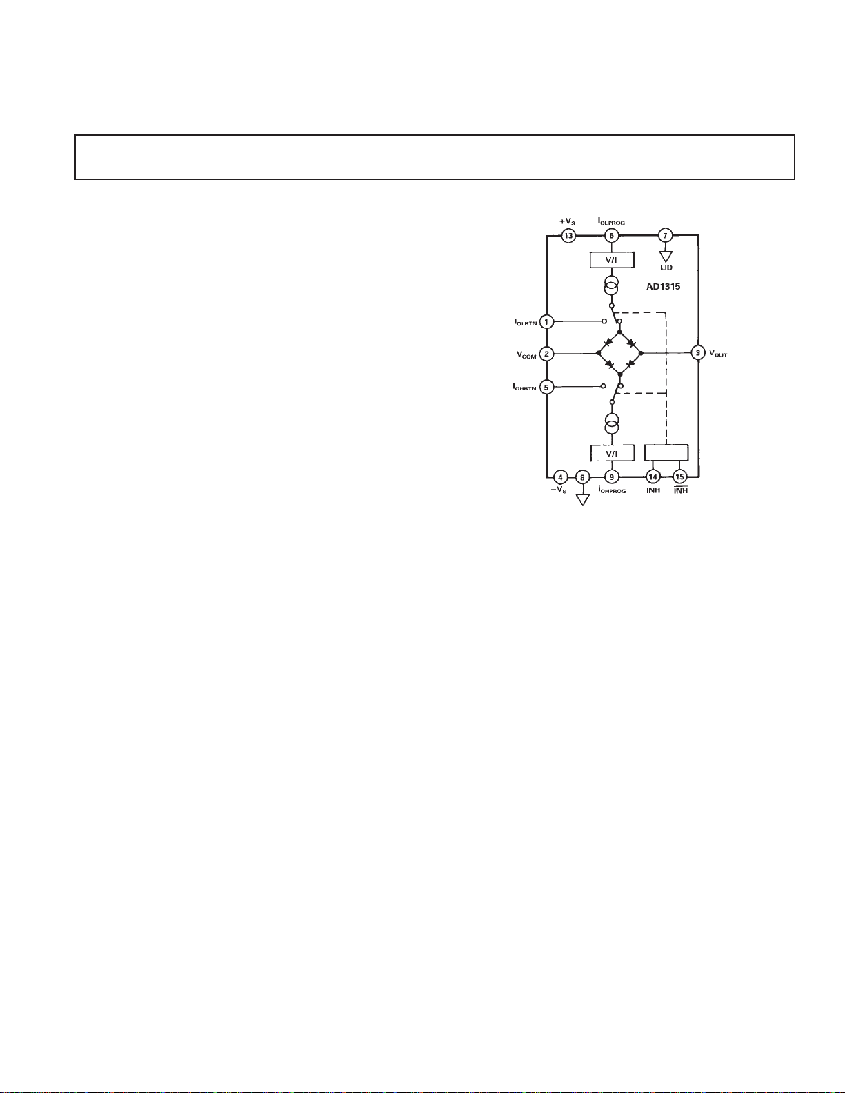
FUNCTIONAL BLOCK DIAGRAM
PRODUCT DESCRIPTION
The AD1315 is a complete, high speed, current switching load
designed for use in linear, digital or mixed signal test systems.
By combining a high speed monolithic process with a unique
surface mount package, this product attains superb electrical
performance while preserving optimum packaging densities in
an ultrasmall 16-lead, hermetically sealed gull wing package.
Featuring current programmability of up to +50 mA, the
AD1315 is designed to force the device under test to source or
sink the programmed I
and IOL currents are determined by applying a corresponding
voltage (5 V = 50 mA) to the I
to-current conversion is performed within the AD1315 thus
allowing the current levels to be set by a standard voltage out
digital-to-analog converter.
The AD1315’s transition from IOH to IOL occurs when the
output voltage of the device under test slews above or below the
programmed threshold, or commutation voltage. The commuta-
OHPROG
and I
and IOL pins. The voltage-
OH
currents. The I
OLPROG
OH
tion voltage is programmable from 2 V to +7 V, covering the
large spectrum of logic devices while able to support the large
current specifications (48 mA) typically associated with line
drivers. To test I/O devices, the active load can be switched into
a high impedance state (Inhibit mode) electrically removing the
active load from the path through the Inhibit mode feature. The
active load leakage current in Inhibit is typically 20 nA.
The Inhibit input circuitry is implemented utilizing high speed
differential inputs with a common-mode voltage range of 7 volts
and a maximum differential voltage of 4 volts. This allows for
the direct interface to the precision of differential ECL timing or
the simplicity of switching the Active Load from a single ended
TTL or CMOS logic source. With switching speeds from IOH
or Io~ into Inhibit of less than 1.5 ns, the AD1315 can be
electrically removed from the signal path “on-the-fly.”
The AD1315 is available in a 16-lead, hermetically sealed gull
wing package and is specified to operate over the ambient commercial temperature range from 0°C to +70°C.
REV. A
Information furnished by Analog Devices is believed to be accurate and
reliable. However, no responsibility is assumed by Analog Devices for its
use, nor for any infringements of patents or other rights of third parties
which may result from its use. No license is granted by implication or
otherwise under any patent or patent rights of Analog Devices.
One Technology Way, P.O. Box 9106, Norwood, MA 02062-9106, U.S.A.
Tel: 617/329-4700 World Wide Web Site: http://www.analog.com
Fax: 617/326-8703 © Analog Devices, Inc., 1997
Page 2

(All measurements made in free air at +258C. +VS = +10 V, –VS = –5.2 V, unless
AD1315–SPECIFICATIONS
otherwise noted.)
AD1315KZ
Parameter Min Typ Max Units Comments
DIFFERENTIAL INPUT CHARACTERISTICS
INH to INH
Input Voltage, Any One Input –3.0 4.0 Volts
Differential Input Range 0.4 ECL 4.0 Volts
Bias Current –2.0 1.0 2.0 mA
Current Program Voltage Range
I
, 0 mA to +50 mA (Sink)
OH
I
, 0 mA to –50 mA (Source)
OL
Input Resistance 50 kΩ
I
, I
OHRTN
V
OCRTN
, V
COM
I
OH
Range –2.0 +7.0 Volts
DUT
, 0 mA to +50 mA 0.5 +7.0 Volts V
Range
2
IOL, 0 mA to –50 mA –2.0 +4.0 Volts V
OUTPUT CHARACTERISTICS
1
1
0 +5.0 Volts
0 +5.0 Volts
–2.0 +7.0 Volts
– V
DUT
COM
3
– V
COM
DUT
Active (Sink/Source) Mode
Transfer Function 10 mA/V See Figure 1
Accuracy See Figure 1
Linearity Error –0.12 +0.12 % FSR
Gain Error –2.0 +2.0 % FSR
Offset Error –1.0 +1.0 mA
Output Current TC 10 µA/°C
Inhibit Mode
Output Capacitance 3.0 pF
Inhibit Leakage –200 20 200 nA
(t
PD1
PD2
3
4
)
4
)
0.5 1.5 ns
1.5 3.0 ns
DYNAMIC PERFORMANCE
Propagation Delay See Figure 2
±I
to INHIBIT (t
MAX
INHIBIT to ±I
MAX
POWER SUPPLIES
to +VS Difference 15.2 15.4 Volts
–V
S
Supply Range
Positive Supply +9.5 +10 +10.5 Volts
Negative Supply –5.45 –5.2 –4.95 Volts
Current
Positive Supply
Negative Supply
Power Dissipation
7
PSRR
NOTES
1
I
OHPROG/IOLPROG
2
I
OHRTN/IOLRTN
3
V
DUT
4
Measured from the ECL crossing to the 10% change in the output current.
5
I
PROGRAM
6
Maximum power dissipation with +VS = +10 V, –VS = 5.2 V, I
7
For a 1% change in +VS or VS, the output current may change a maximum of 0.05% of Full Scale Range (FSR).
Specifications subject to change without notice.
should be connected to V
= –2 V to +7 V, C
= ±50 mA.
5
5
6
voltage range may be extended to –100 mV due to a possible 1 mA offset current.
= 10 pF, R
TOTAL
to minimize power dissipation.
COM
= 10 Ω. For inhibit leakage tests, V
DUT
PROGRAM
5
+70
5
–100
50 mA, V
+85 +100 mA
–85 –70 mA
1.3 1.54
= 0 V to +5.9 V, IOH = –4 mA, IOL = +4 mA, T
DUT
= V
DUT
= 0 V.
COM
0.05 %/%
CASE
= +36°C.
>1 V
>1 V
–2–
REV. A
Page 3
AD1315
ABSOLUTE MAXIMUM RATINGS
1
Power Supply Voltage
+V
to GND . . . . . . . . . . . . . . . . . . . . . . . . . . . . . . . +12 V
S
–V
to GND . . . . . . . . . . . . . . . . . . . . . . . . . . . . . . . . –11 V
S
Difference from +V
to –VS . . . . . . . . . . . . . . . . . . . . . 16 V
S
Inputs
Difference from INH to INH . . . . . . . . . . . . . . . . . . . . . 5 V
INH, INH . . . . . . . . . . . . . . . . . . +V
V
, V
COM
I
, IOH Program Voltage . . . . . . . . +VS – 15 V, –VS + 15 V
OL
. . . . . . . . . . . . . . . +VS – 13.1 V, –VS + 13.2 V
DUT
– 13.4 V, –VS + 11 V
S
Operating Temperature Range . . . . . . . . . . . . . . . 0 to +70°C
Storage Temperature Range . . . . . . . . . . . . –65°C to +125°C
Lead Temperature Range (Soldering 20 sec)
2
. . . . . . .+300°C
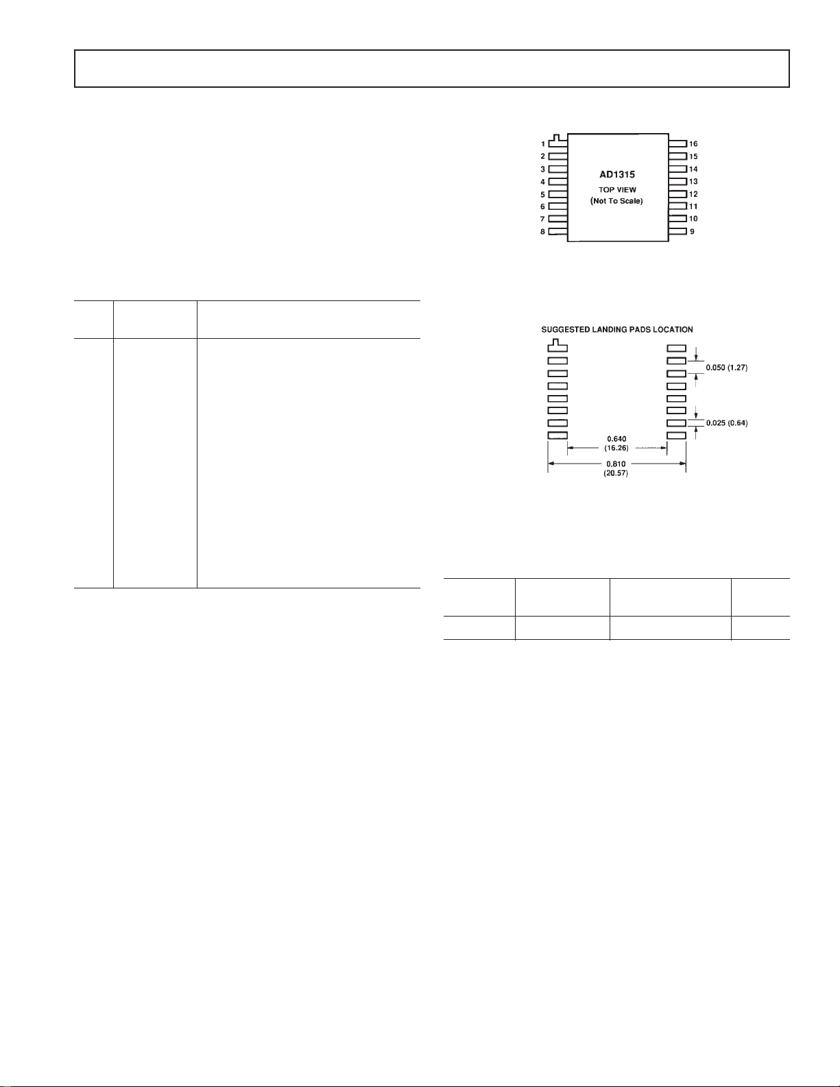
Pin
No. Symbol Function
1I
2V
3V
4–V
5I
6I
OLRTN
COM
DUT
S
OHRTN
OLPROG
Logic Low Current Return
Communication Voltage
Load/Dot Connection
Negative Supply
Logic High Current Return
Logic Low Current Program Voltage
7 LID Lid Connection (Internal)
8 GND Ground
9I
OHPROG
Logic High Current Program Voltage
10 N/C No Connection
11 N/C No Connection
12 N/C No Connection
13 +V
S
Positive Supply
14 INH Inhibit
15 INH Inhibit
16 N/C No Connection
1
Stresses above those listed under Absolute Maximum Ratings may cause permanent damage to the device. This is a stress rating only; functional operation of the
device at these or any other conditions above those indicated in the operational
sections of this specification is not implied. Exposure to absolute maximum rating
conditions for extended periods may affect device reliability.
2
To ensure lead coplanarity (±0.002 inches) and solderability, handling with bare
hands should be avoided and the device should be stored in an environment at
24°C, ±5°C (75°F, ±10°F) with relative humidity not to exceed 65%.
CONNECTION DIAGRAM
SUGGESTED PAD LOCATION
Dimensions shown in inches and (mm).
ORDERING GUIDE
Temperature Package Package
Model Range Description Option*
AD1315KZ 0 to +70°C 16-Lead Gull Wing Z-16B
*Z = Leaded Chip Carrier (Ceramic).
REV. A
–3–
Page 4

AD1315
DEFINITION OF TERMS
Gain
The measured transconductance.
Gain =
(@ 5V Input )− I
I
OUT
V
PROG
(@ 5V ) − V
(@ 0.2V Input )
OUT
(@ 0.2V)
PROG
where:
values are measured at IOL/IOH PROG
V
PROG
Gain Error
The difference between the measured transconductance and the
ideal expressed as a % of full-scale range.
Ideal Gain = 10 mA/V
Gain Error =
Ideal Gain − Actual Gain
Ideal Gain
×100
Offset Error
Offset Error is measured by setting the I
inputs to 0.2 V and measuring I
. Since both IOH and I
OUT
OHPROG
or I
OLPROG
OL
outputs are unipolar, this small initial offset of 2 mA must be set
to allow for measurement of possible negative offset. With a gain
of 10 mA/V, a 0.2 V input should yield an output of ±2 mA. The
difference between the observed output and the ideal ±2mA
output is the offset error.
Offset Error = I
(@ 0.2 V) – Gain 3 V
OUT
(@ 0.2 V)
PROG
Linearity Error
The deviation of the transfer function from a straight line defined by Offset and Gain expressed as a % of FSR.
I
(calc) = Gain 3 V
OUT
(@ set point) + Offset
PROG
where:
set point = V
I
OUT
Linearity Error
(from 0.2 V to 5 V)
PROG
(FSR) = Gain 3 V
(measured ) − I
I
OUT
I
(@ 5 V) + Offset
PROG
(FSR)
OUT
OUT
(calc)
×100
Figure 1. Definition of Terms
Figure 3. IOL, IOH Offset Current vs.
Temperature
Figure 2. Timing Diagram for Inhibit Transition
Figure 4. IOL, IOH Gain Error vs.
Temperature
Figure 5. I
, IOH Linearity Error vs.
OL
Current Program Voltage
–4–
REV. A
Page 5

AD1315
Figure 6. +I
MAX
, –I
to Inhibit
MAX
Propagation Delay vs. Temperature
Figure 8. Inhibit Mode Leakage Current vs. Case Temperature
Figure 7. Inhibit to +I
MAX
, –I
MAX
Propagation Delay vs. Temperature
REV. A
Figure 9. AD1315 DC Test Circuit
Figure 10. AD1315 Propagation Delay Test Circuit
–5–
Page 6

AD1315
FUNCTIONAL DESCRIPTION
The AD1315 is a complete high speed active load designed for
use in general purpose instrumentation and digital functional
test equipment. The function of the active load is to provide
independently variable source and sink currents for the device to
be tested.
The equivalent circuit for the AD1315 is shown in Figure 11.
An active load performs the function of loading the output of
the device under test with a programmed I
currents are independently programmable. V
tation voltage point at which the load switches from source to
sink mode. The active load may also be inhibited, steering current to the I
OLRTN
and I
pins, effectively disconnecting it
OHRTN
from the test pin.
The AD1315 accepts differential digital signals at its inhibit
inputs ensuring precise timing control and high noise immunity.
The wide inhibit input voltage range allows for ECL power
supplies of –5.2 V and 0 V, –3.2 V and +2 V, and 0 V and +5 V.
Where speed and timing accuracy are less important, TTL or
CMOS logic levels may be used to toggle the Inhibit inputs of
the AD1315. Single ended operation is possible by biasing one
of the inputs to approximately +1.3 V for TTL or V
CMOS. Care should be taken to observe the 4 V maximum
allowable input voltage.
The I
and IOL programming inputs accept 0 V to +5 V analog
OH
inputs, corresponding to 0 to 50 mA output currents. The V
input, which sets the IOH/IOL switch point, may be set anywhere
within the input range of –2 V to +7 V.
or IOL. These
OH
is the commu-
COM
CC
/2 for
COM
Figure 12. Allowable Current Range for IOH, IOL vs. V
Ideally, the commutation point set at V
would provide in-
COM
DUT
stantaneous current sink/source switching. Because of I/V
characteristics of the internal bridge diodes, this is not the case.
To guarantee full current switching at the DUT, at least a 1 volt
difference between V
COM
and V
must be maintained in
DUT
steady state conditions. Because of the relatively fast edge rates
exhibited by typical logic device outputs, this should not be a
problem in normal ATE applications.
INHIBIT MODE LEAKAGE
The AD1315’s inhibit-mode leakage current changes with both
temperature and bias levels. There are two major contributing
effects: transistor reverse-bias collector-base leakage and reverse
leakage in the Schottky-diode bridge. Leakage variations with
V
arise primarily from transistor collector-base leakage,
DUT
while both effects contribute to leakage current temperature
variations. Inhibit-mode leakage is weakly dependent on V
and decreases slightly as the difference between V
DUT
COM
and V
COM
is reduced. Figure 8 shows typical AD1315 inhibit leakage current as a function of V
and temperature.
DUT
Figure 11. Block Diagram
V
VOLTAGE RANGE
DUT
In Figure 12, V
mums are plotted versus DUT voltage. In the I
higher than V
starts to saturate at approximately –1.5 V. In the I
(V
lower than V
DUT
range, IOH and IOL typical current maxi-
DUT
), the load will sink 50 mA, until its output
COM
), the load will source 50 mA until its
COM
mode (V
OH
mode
OL
DUT
output starts to saturate at approximately +5.5 V. At +7 V, the
source current will be close to zero.
THERMAL CONSIDERATIONS
The AD1315 is provided in a 0.550" 3 0.550", 16-lead (bottom
brazed) gull wing, surface mount package with a θ
of 10°C/W
JC
(typ). Thermal resistance (case-to-ambient) vs. air flow for the
AD1315 in this package is shown in Figure 13. The data presented is for a ZIF socketed device. For PCB mounted devices
(w/30 mils clearance) the thermal resistance should be ~3 to 7%
lower with air flows below 320 lfm
ment in thermal resistance vs. air flow starts to flatten out just
above 400 lfm
NOTES
1
Ifm is air flow in linear feet/minute.
2
For convection cooled systems, the minimum recommended airflow is 400 lfm.
(2)
.
(1)
. Notice that the improve-
Figure 13. Case-to-Ambient Thermal Resistance vs.
Air Flow
–6–
REV. A
Page 7

AD1315
APPLICATIONS
The AD1315 has been optimized to function as an active load
in an ATE test system. Figure 14 shows a block diagram illustrating the electronics behind a single pin of a high speed digital
functional test system with the ability to test I/O pins on logic
devices. The AD1315 active load, AD1321 or AD1324 pin
driver, AD1317 high speed dual comparator and the AD664
quad 12-bit voltage DAC would comprise the pin electronic
portion of the test system. Such a system could operate at
100 MHz with the AD1321 (200 MHz with the AD1324) in a
data mode or 50 MHz (100 MHz) in the I/O mode.
The V
With DUT output voltage above V
rent (I
input sets the commutation voltage of the active load.
COM
). With DUT output voltage below V
OH
, the load will sink cur-
COM
, the load will
COM
source current (I
). Like the IOH and IOL return lines, the V
OL
COM
must be able to sink or source 50 mA, therefore a standard op
amp will not suffice. An op amp with an external complementary output stage or a high power op amp such as the AD842
will work well here. A typical application is shown in Figure 15.
LAYOUT CONSIDERATIONS
I
OHRTN
and I
may be connected to any potential between
OLRTN
–2 V and +7 V. These return points must be able to source or
sink 50 mA, since the I
and IOL programmed currents are
OH
diverted here in the inhibit mode. The RTNs may be connected
to a suitable GND. However, to keep transient ground currents
to a minimum, they are typically tied to the V
programming
COM
voltage point.
REV. A
Figure 14. High Speed Digital Test System Block Diagram
Figure 15. Suggested I
OHRTN
, I
OLRTN
, V
COM
Hookup
–7–
Page 8

AD1315
EVALUATION BOARD
The AD1315 Evaluation Board allows the designer to easily
evaluate the performance of the AD1315 and its suitability for
the specific application. The AD1315EB includes a mounted
AD1315KZ active load, an ECL input buffer for Inhibit and the
oscilloscope probe jacks necessary to properly analyze the true
performance of the AD1315KZ. An equipment list is provided
in order to minimize variations due to test setups.
C1337a–1–5/97
Figure 16. AD1315EB Evaluation Board Circuit
OUTLINE DIMENSIONS
Dimensions shown in inches and (mm).
16-Lead Gull Wing
(Z-16B)
PRINTED IN U.S.A.
–8–
REV. A
 Loading...