

Datasheet ACT-SF512K32N-39P1T, ACT-SF512K32N-39P1Q, ACT-SF512K32N-39P1M, ACT-SF512K32N-39P1I, ACT-SF512K32N-39P1C Datasheet (ACT)
...Page 1
eroflex Circuit Technology - Advanced Multichip Modules © SCD3852 REV A 5/20/98
F
E
I
D
C
E
R
T
A
E
R
O
F
L
E
X
L
A
B
S
I
N
C
.
ACT-SF512K32 High Speed
512Kx32 SRAM / 512Kx32 Flash
Multichip Module
FEATURES
■
4 – 512K x 8 SRAMs & 4 – 512K x 8 Flash Die in
One MCM
■ Access Times of 25ns, 35ns (SRAM) and
60ns, 70ns, 90ns (Flash)
■ Organized as 512K x 32 of SRAM and 512K x 32
of Flash Memory with Common Data Bus
■ Low Power CMOS
■ Input and Output TTL Compatible Design
■ MIL-PRF-38534 Compliant MCMs Available
■ Decoupling Capacitors and Multiple Grounds for
Low Noise
■ Commercial, Industrial and Military Temperature
Ranges
■ Industry Standard Pinouts
■ TTL Compatible Inputs and Outputs
■ Packaging – Hermetic Ceramic
● 66–Lead, PGA-Type, 1.385"SQ x 0.245"max,
Aeroflex code# "P1,P5 with/without shoulders)"
● 68–Lead, Dual-Cavity CQFP(F2), 0.88"SQ x
.20"max (.18 max thickness available, contact
factory for details) (Drops into the 68 Lead
JEDEC .99"SQ CQFJ footprint)
CIRCUIT TECHNOLOGY
www.aeroflex.com
FLASH MEMORY FEATURES
■ Sector Architecture (Each Die)
● 8 Equal Sectors of 64K bytes each
● Any combination of sectors can be erased with one
ISO
900
1
I
command sequence
■ +5V Programing, +5V Supply
■ Embedded Erase and Program Algorithms
■ Hardware and Software Write Protection
■ Page Program Operation and Internal Program
Control Time.
■ 10,000 Erase/Program Cycles
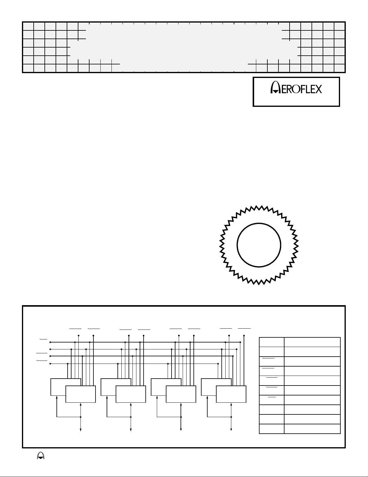
Block Diagram – PGA Type Package(P1 & P5) & CQFP(F2)
FWE4 SWE4 PIN DESCRIPTION
I/O
0-31 Data I/O
A
0–18 Address Inputs
FWE
1-4 Flash Write Enables
SWE
1-4 SRAM Write Enables
512K X 8 FLASH
512K X 8 SRAM
FCE
SCE
OE
NC Not Connected
V
CC Power Supply
GND Ground
Flash Chip Enable
SRAM Chip Enable
Output Enable
OE
A0–A18
SCE
FCS
FWE1
512K X 8 FLASH
512K X 8 SRAM
SWE1
FWE2 SWE2
512K X 8 FLASH
512K X 8 SRAM
I/O8-15 I/O16-23I/O0-7 I/O24-31
FWE3 SWE3
512K X 8 FLASH
512K X 8 SRAM
Page 2
Absolute Maximum Ratings
Symbol Rating Range Units
-55 to +125 °C
-65 to +150 °C
-0.5 to +7 V
300 °C
T
T
STG
V
T
Operating Temperature
C
Storage Temperature
Maximum Signal Voltage to Ground
G
Maximum Lead Temperature (10 seconds)
L
Parameter
Flash Data Retention 10 Years
Flash Endurance (Write/Erase Cycles) 10,000
Normal Operating Conditions
Symbol Parameter Minimum Maximum Units
V
CC
V
IH
V
IL
Power Supply Voltage
Input High Voltage
Input Low Voltage
+4.5 +5.5 V
+2.2 V
+ 0.3 V
CC
-0.5 +0.8 V
Capacitance
(V
= 0V, f = 1MHz, TC = 25°C)
IN
Symbol Parameter Maximum Units
AD
C
C
C
WE1-4
C
C
A0 – A18 Capacitance
OE
OE Capacitance
F/S Write Enable Capacitance
CE
F/S Chip Enable Capacitance
I/O
I/O0 – I/O31 Capacitance
This parameter is guaranteed by design but not tested
80 pF
80 pF
30 pF
50 pF
30 pF
DC Characteristics
(VCC = 5.0V, VSS = 0V, TC = -55°C to +125°C)
Parameter Sym Conditions Min Max Units
I
Input Leakage Current
Output Leakage Current
SRAM Operating Supply Current x 32
Mode
I
CC
Standby Current
SRAM Output Low Voltage
SRAM Output High Voltage
Flash Vcc Active Current for Read (1)
Flash Vcc Active Current for Program
or Erase (2)
Flash Output Low Voltage
Flash Output High Voltage
Flash Low Vcc Lock Out Voltage
Notes: 1) The ICC current listed includes both the DC operating current and the frequency dependent component (at 5MHz). The
frequency component typically is less than 2mA/MHz, with OE
erase) is in progress 3) DC test conditions: V
V
V
I
I
V
V
V
IL = 0.3V, VIH = VCC - 0.3V
VCC = Max, VIN=0toV
LI
FCE = SCE = VIH, OE = V
I
LO
V
=0toV
OUT
SCE
x32
I
SB
OL
OH
CC1
CC2
OL
OH1
LKO
= VIL, OE = VIH, f = 5MHz, VCC =
Max, FCE
FCE = SCE = VIH, OE = VIH, f = 5MHz,
= Max
V
CC
IOL = 8 mA, VCC = Min, FCE = V
IOH = -4.0 mA, , VCC = Min, FCE = V
FCE = VIL, OE = VIH, SCE = V
FCE = VIL, OE = VIH, SCE = V
IOL = 12 mA, VCC = Min, SCE = V
IOH = -2.5 mA, , VCC = Min, SCE = V
CC
= V
IH
at VIH 2) ICC active while Embedded Algorithim (program or
CC
IH,
IH
IH
IH
IH
IH
IH
2.4 V
0.85 x VCC V
3.2 4.2 V
10 µA
10 µA
550 mA
80 mA
0.4 V
260 mA
300 mA
0.45 V
Aeroflex Circuit Technology SCD3852 REV A 5/20/98 Plainview NY (516) 694-6700
2
Page 3
SRAM AC Characteristics
(VCC = 5.0V, VSS= 0V, Tc= -55°C to +125°C)
Read Cycle
Parameter Symbol
Read Cycle Time
Address Access Time
Chip Select Access Time
Output Hold from Address Change
Output Enable to Output Valid
Chip Select to Output in Low Z *
Output Enable to Output in Low Z *
Chip Deselect to Output in High Z *
Output Disable to Output in High Z *
* Parameters guaranteed by design but not tested
Write Cycle
Parameter Symbol
Write Cycle Time
Chip Select to End of Write
Address Valid to End of Write
Data Valid to End of Write
Write Pulse Width
Address Setup Time
Output Active from End of Write *
Write to Output in High Z *
Data Hold from Write Time
Address Hold Time
* Parameters guaranteed by design but not tested
t
t
t
ACE
t
t
t
CLZ
t
OLZ
t
CHZ
t
OHZ
t
WC
t
CW
t
AW
t
DW
t
WP
t
t
OW
t
WHZ
t
DH
t
RC
AA
OH
OE
AS
AH
–025
Min Max
–035
Min Max
Units
25 35 ns
25 35 ns
25 35 ns
0 0 ns
12 25 ns
2 4 ns
0 0 ns
12 15 ns
12 15 ns
–025
Min Max
–035
Min Max
Units
25 35 ns
17 25 ns
17 25 ns
13 20 ns
17 25 ns
2 2 ns
4 4 ns
13 15 ns
0 0 ns
0 0 ns
Truth Table
Mode SCE OE SWE Data I/O Power
Standby H X X High Z Standby
Read L L H Data Out Active
Output Disable L H H High Z Active
Write L X L Data In Active
Aeroflex Circuit Technology SCD3852 REV A 5/20/98 Plainview NY (516) 694-6700
3
Page 4
Timing Diagrams — SRAM
Read Cycle Timing Diagrams
Read Cycle 1 (SCE = OE = VIL, SWE = VIH)
tRC
A0-18
tAA
tOH
DI/O
Read Cycle 2 (SWE = VIH)
tRC
A0-18
tAA
SCE
OE
DI/O
tCLZ
SEE NOTE
tOLZ
SEE NOTE
High Z
tACE
OE
t
SEE NOTE
Data Valid
Data ValidPrevious Data Valid
tCHZ
t
OHZ
SEE NOTE
Write Cycle Timing Diagrams
Write Cycle (SWE Controlled, OE = VIH)
tWC
A0-18
tAW tAH
tWHZ
tCW
tDW
Data Valid
tWC
tAW
tCW
tWP
tDW
Data Valid
SCE
tAS tWP
SWE
DI/O
Write Cycle (SCE
A0-18
tAS
SCE
SWE
DI/O
SEE NOTE
Controlled, OE = VIH )
tOW
tDH
tAH
tDH
UNDEFINED
DON’T CARE
Note: Guaranteed by design, but not tested.
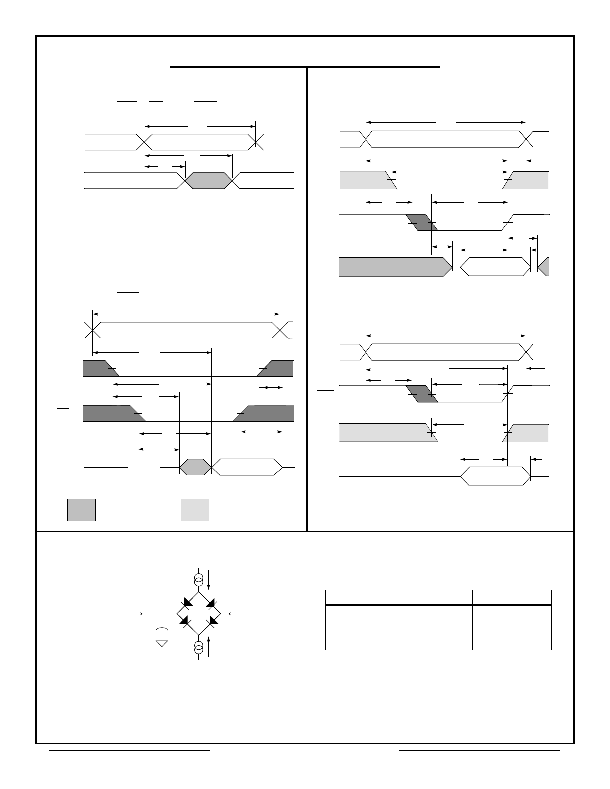
AC Test Circuit
Current Source
IOL
Z ~ 1.5 V (Bipolar Supply)
To Device Under Test
C
L = 50 pF
Current Source
V
OH
I
Input and Output Timing Reference Level 1.5 V
Notes:
1) V
Z is programmable from -2V to +7V. 2) IOL and IOH programmable from 0 to 16 mA. 3) Tester Impedance
Z
O =75Ω. 4) VZ is typically the midpoint of VOH and VOL. 5) IOL and IOH are adjusted to simulate a typical resistance
load circuit. 6) ATE Tester includes jig capacitance.
Aeroflex Circuit Technology SCD3852 REV A 5/20/98 Plainview NY (516) 694-6700
4
AC Test Conditions
Parameter Typical Units
Input Pulse Level 0 – 3.0 V
Input Rise and Fall 5 ns
Page 5

Flash AC Characteristics – Read Only Operations
Parameter
Read Cycle Time
Address Access Time
Chip Enable Access Time
Output Enable to Output Valid
Chip Enable to Output High Z (1)
Output Enable High to Output High Z(1)
Output Hold from Address, CE
Note 1. Guaranteed by design, but not tested
or OE Change, Whichever is First
(Vcc = 5.0V, Vss = 0V, Tc = -55°C to +125°C)
Symbol
JEDEC Stand’d
t
AVAV tRC 60 70 90 ns
AVQV tACC 60 70 90 ns
t
ELQV tCE 60 70 90 ns
t
GLQV tOE 30 35 35 ns
t
EHQZ tDF 20 20 20 ns
t
GHQZ tDF 20 20 20 ns
t
t
AXQX tOH 0 0 0 ns
–60
Min Max
–70
Min Max
–90
Min Max
Units
Flash AC Characteristics – Write / Erase / Program Operations, FWE Controlled
(Vcc = 5.0V, Vss = 0V, Tc = -55°C to +125°C)
Parameter
Write Cycle Time
Chip Enable Setup Time
Write Enable Pulse Width
Address Setup Time
Data Setup Time
Data Hold Time
Address Hold Time
Write Enable Pulse Width High
Duration of Byte Programming Operation
Sector Erase Time
Read Recovery Time before Write
Vcc Setup Time
Chip Programming Time
Chip Enable Hold Time
Chip Erase Time
1. Toggle and Data Polling only.
Symbol
JEDEC Stand’d
t
AVAC tWC 60 70 90 ns
ELWL tCE 0 0 0 ns
t
WLWH tWP 40 45 45 ns
t
AVWL tAS 0 0 0 ns
t
DVWH tDS 40 45 45 ns
t
WHDX tDH 0 0 0 ns
t
WLAX tAH 45 45 45 ns
t
WHWL tWPH 20 20 20 ns
t
WHWH1 14 TYP 14 TYP 14 TYP µs
t
WHWH2 30 30 30 Sec
t
tGHWL 0 0 0 µs
VCE 50 50 50 µs
t
1
OEH
t
WHWH3 120 120 120 Sec
t
–60
Min Max
50 50 50 Sec
10 10 10 ns
–70
Min Max
–90
Min Max
Flash AC Characteristics – Write / Erase / Program Operations, FCE Controlled
(Vcc = 5.0V, Vss = 0V, Tc = -55°C to +125°C)
Parameter
Write Cycle Time
Write Enable Setup Time
Chip Enable Pulse Width
Address Setup Time
Data Setup Time
Data Hold Time
Address Hold Time
Chip Enable Pulse Width High
Duration of Byte Programming
Sector Erase Time
Read Recovery Time
Chip Programming Time
Chip Erase Time
Symbol
JEDEC Stand’d
t
AVAC tWC 60 70 90 ns
WLEL tWS 0 0 0 ns
t
ELEH tCP 40 45 45 ns
t
AVEL tAS 0 0 0 ns
t
DVEH tDS 40 45 45 ns
t
EHDX tDH 0 0 0 ns
t
ELAX tAH 45 45 45 ns
t
EHEL tCPH 20 20 20 ns
t
WHWH1 14 TYP 14 TYP 14 TYP µs
t
WHWH2 30 30 30 Sec
t
tGHEL 0 0 0 ns
WHWH3 120 120 120 Sec
t
–60
Min Max
50 50 50 Sec
–70
Min Max
Min Max
–90
Units
Units
Aeroflex Circuit Technology SCD3852 REV A 5/20/98 Plainview NY (516) 694-6700
5
Page 6

AC Waveforms for Flash Memory Read Operations
tRC
Addresses Addresses Stable
tACC
FCE
tDF
OE
FWE
Outputs
Write/Erase/Program
Operation for Flash Memory, F
Addresses
FCE
OE
5555H PA
tWC
tAS
tGHWL
tAH
tOE
WE Controlled
Data
Polling
Output Valid
PA
tOHtCE
High ZHigh Z
tRC
tWP
FWE
Data
5.0V
Notes:
1. PA is the address of the memory location to be programmed.
2. PD is the data to be programmed at byte address.
3. D7 is the 0utput of the complement of the data written to the deviced.
4. Dout is the output of the data written to the device.
5. Figure indicates last two bus cycles of four bus cycle sequence.
Aeroflex Circuit Technology SCD3852 REV A 5/20/98 Plainview NY (516) 694-6700
tCE
tDS
tWPH
tDH
t
WHWH1
6
D7
tOE
tDF
DOUTPDAOH
tOH
tCE
Page 7

AC Waveforms Chip/Sector
Erase Operations for Flash Memory
AH
t
Data
Polling
Addresses
FCE
OE
FWE
Data
CC
V
5555H
tAS
tGHWL
tWP
tWPH
tCE
tDH
55H AAH80H 55H 10H/30HAAH
tDS
tVCE
Notes:
1. SA is the sector address for sector erase.
5555H 5555H SA2AAAH 2AAAH
AC Waveforms for Data Polling
During Embedded Algorithm Operations for Flash Memory
FCE
OE
FWE
tCH
DQ7
DQ0-DQ6
tOEH
tOE
tDF
tCE
tOH
*
DQ
7
DQ7=
Valid Data
tWHWH1 or 2
DQ0–DQ6=Invalid
DQ0–DQ6
Valid Data
tOE
* DQ7=Valid Data (The device has completed the Embedded operation).
High Z
Aeroflex Circuit Technology SCD3852 REV A 5/20/98 Plainview NY (516) 694-6700
7
Page 8

Write/Erase/Program Operation for Flash Memory, FCE Controlled
Data
Polling
Addresses
FCE
OE
FWE
Data
5.0V
5555H
tWC
PA
tAHtAS
tGHWL
tWS
tCP
tCPH
t
WHWH1
tDH
tDS
Notes:
1. PA is the address of the memory location to be programmed.
2. PD is the data to be programmed at byte address.
is the 0utput of the complement of the data written to the device.
3. D7
OUT is the output of the data written to the device.
4. D
5. Figure indicates last two bus cycles of four bus cycle sequence.
PA
D7
DOUTPDAOH
Aeroflex Circuit Technology SCD3852 REV A 5/20/98 Plainview NY (516) 694-6700
8
Page 9

Pin Numbers & Functions
All dimensions in inches
66 Pins — PGA-Type
Pin # Function Pin # Function Pin # Function Pin # Function
1 I/O
2 I/O9 19 Vcc 36 I/O26 53 SWE3
3 I/O10 20 FCE 37 A7 54 GND
4 A
5 A16 22 I/O3 39 SWE1 56 I/O31
6 A11 23 I/O15 40 A13 57 I/O30
7 A0 24 I/O14 41 A8 58 I/O29
8 A18 25 I/O13 42 I/O16 59 I/O28
9 I/O0 26 I/O12 43 I/O17 60 A1
10 I/O1 27 OE 44 I/O18 61 A2
11 I/O2 28 A17 45 VCC 62 A3
12 FWE2 29 FWE1 46 SWE4 63 I/O23
13 SWE2 30 I/O7 47 FWE4 64 I/O22
14 GND 31 I/O6 48 I/O27 65 I/O21
15 I/O11 32 I/O5 49 A4 66 I/O20
16 A10 33 I/O4 50 A5
17 A9 34 I/O24 51 A6
8 18 A15 35 I/O25 52 FWE3
14 21 SCE 38 A12 55 I/O19
"P1" — 1.385" SQ PGA Type Package Standard (with shoulders on Pins 1, 11, 56 & 66)
"P5" — 1.385" SQ PGA Type Special Order Package (without shoulders
)
Bottom View (P1 & P5)
Side View
(P1)
.245
MAX
.025
.035
.145
MIN
.100
TYP
.020
.016
Side View
(P5)
.220
MAX
.165
MIN
Pin 56
.100 TYP
.020
.016
Pin 66
1.400 SQ
MAX
1.000
TYP
.600
TYP
.100 TYP
Pin 1
1.000
TYP
Pin 11
Aeroflex Circuit Technology SCD3852 REV A 5/20/98 Plainview NY (516) 694-6700
9
Page 10

Pin Numbers & Functions
68 Pins — Dual-Cavity CQFP
Pin # Function Pin # Function Pin # Function Pin # Function
1 GND 18 GND 35 OE
2 SWE
3 19 I/O8 36 SWE2 53 FI/O23
3 A5 20 I/O9 37 A17 54 FI/O22
4 A4 21 I/O10 38 FWE2 55 FI/O21
5 A3 22 I/O11 39 FWE3 56 FI/O20
6 A2 23 I/O12 40 FWE4 57 FI/O19
7 A1 24 I/O13 41 A18 58 FI/O18
8 A0 25 I/O14 42 SCE 59 FI/O17
9 NC 26 I/O15 43 SWE1 60 FI/O16
10 I/O0 27 Vcc 44 FI/O31 61 VCC
11 I/O1 28 A11 45 FI/O30 62 A10
12 I/O2 29 A12 46 FI/O29 63 A9
13 I/O3 30 A13 47 FI/O28 64 A8
14 I/O4 31 A14 48 FI/O27 65 A7
15 I/O5 32 A15 49 FI/O26 66 A6
16 I/O6 33 A16 50 FI/O25 67 FWE1
17 I/O7 34 FCE 51 FI/O24 68 SWE4
52 GND
Package Outline — Dual-Cavity CQFP "F2"
Top View
.990 SQ
±.010
.890 SQ
Pin 9 Pin 61
Pin 10
Pin 26
MAX
.800 REF
Pin 60
±.002
Pin 44
Pin 43Pin 27
.015
.050
TYP
*.200 MAX
+3°/-3°
.040
±.005
See Detail “A”
.010 ±.002
.010 R
REF
Detail “A”
.010 REF
.010 REF
.010 ±.005
*.180 MAX available, call factory for details
All dimensions in inches
Aeroflex Circuit Technology SCD3852 REV A 5/20/98 Plainview NY (516) 694-6700
10
Page 11

CIRCUIT TECHNOLOGY
Ordering Information
Model Number DESC Part Number Speed Package
ACT-SF512K32N–26P1X
ACT-SF512K32N–37P1X
ACT-SF512K32N–39P1X
ACT-SF512K32N–26F2X
ACT-SF512K32N–37F2X
ACT-SF512K32N–39F2X
Note: (S) = Speed for SRAM, (F) = Speed for FLASH
ACT– SF 512K 32 N– 26 P1 M
Aeroflex Circuit
Technology
Memory Type
SF = SRAM Flash Combo Module
Memory Depth, Locations
Memory Width, Bits
Pinout Options
N = None
Memory Speed (Code)
26 = 25ns SRAM / 60ns FLASH
37 = 35ns SRAM / 70ns FLASH
39 = 35ns SRAM / 90ns FLASH
TBD 25(S) / 60(F) ns 1.385"sq PGA-Type
TBD 35(S) / 70(F) ns 1.385"sq PGA-Type
TBD 35(S) / 90(F) ns 1.385"sq PGA-Type
TBD 25S) / 60(F) ns .88"sq CQFP
TBD 35(S) / 70(F) ns .88"sq CQFP
TBD 35(S) / 90(F) ns .88"sq CQFP
Part Number Breakdown
C = Commercial Temp, 0°C to +70°C
I = Industrial Temp, -40°C to +85°C
T = Military Temp, -55°C to +125°C
M = Military Temp, -55°C to +125°C Screened
Q = MIL-PRF-38534 Compliant/SMD
F2 = 0.88"SQ 68 Leads Dual-Cavity CQFP
P1 = 1.385"SQ PGA 66 Pins W/Shoulder
P5 = 1.385"SQ PGA 66 Pins WO/Shoulder
Screening
Package Types & Sizes
Surface Mount Packages
Thru-Hole Packages
*
* Screened to the individual test methods of MIL-STD-883
Aeroflex Circuit Technology
35 South Service Road
Plainview New York 11830
Aeroflex Circuit Technology SCD3852 REV A 5/20/98 Plainview NY (516) 694-6700
Toll Free Inquiries: 1-(800) 843-1553
11
Telephone: (516) 694-6700
FAX: (516) 694-6715
 Loading...