

Datasheet ACT-S512K8N-055P4Q, ACT-S512K8N-055F4Q, ACT-S512K8N-055F3Q, ACT-S512K8N-045P4Q, ACT-S512K8N-045F4Q Datasheet (ACT)
...Page 1
www.aeroflex.com
eroflex Circuit Technology - Advanced Multichip Modules © SCD1664 REV C 5/10/00
Features
ACT–S512K8 High Speed
4 Megabit Monolithic SRAM
■ Low Power Monolithic CMOS 512K x 8 SRAM
■ Full Military (-55°C to +125°C) Temperature Range
■ Input and Output TTL Compatible Design
■ Fast 17,20,25,35,45 & 55ns Maximum Access Times
■ +5 V Power Supply
■ MIL-PRF-38534 Compliant MCMs Available
■ Industry Standard Pinouts
■ Packaging – Hermetic Ceramic
● 36 Lead, .92" x .51" x .13" Flat Package (FP), Aeroflex code# "F3"
● 36 Lead, .92" x .43" x .184" Small Outline J lead (CSOJ),
Aeroflex code# "F4"
(.155 MAX thickness available, contact factory for details)
● 32 Lead, 1.6" x .60" x .20" Dual-in-line (DIP), Aeroflex code# "P4"
■ DESC SMD# 5962–95613 Released(F3,F4,P4)
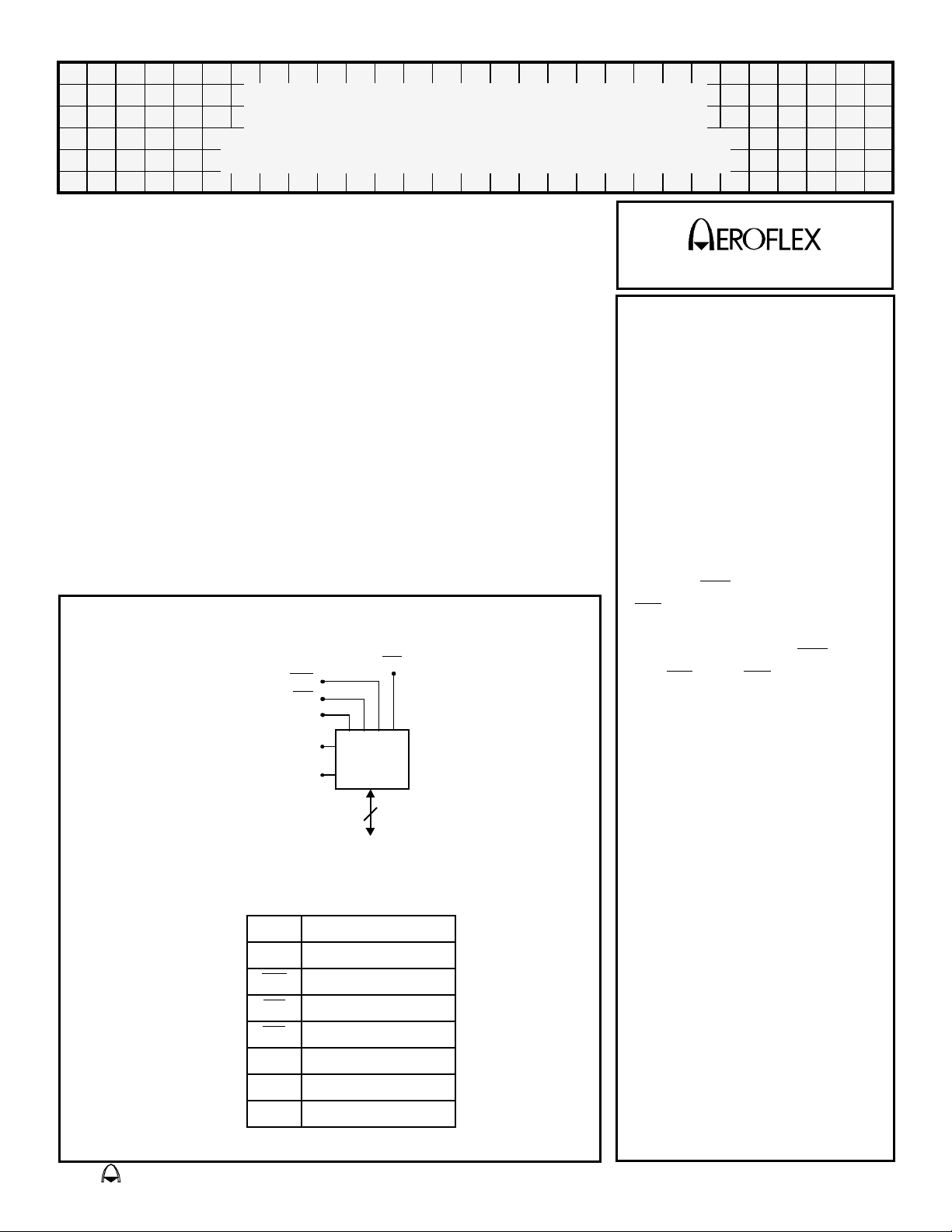
Block Diagram – Flat Package(F3,F16), DIP(P4) & CSOJ(F4)
CE
WE
OE
A0 – A18
Vss
Vcc
512Kx8
8
I/O0-7
CIRCUIT TECHNOLOGY
General Description
The ACT–S512K8 is a high
speed, 4 Megabit CMOS
Monolithic SRAM designed for
full temperature range military,
space, or high reliability mass
memory and fast cache
applications.
The MCM is input and output
TTL compatible. Writing is
executed when the write
enable (WE
(CE
) inputs are low and output
enable (OE) is high.Readingis
accomplished when WE
and CE
Access time grades of 17ns,
20ns, 25ns, 35ns, 45ns and
55ns maximum are standard.
The +5 Volt power supply
version is standard and +3.3
Volt lower power model is a
future optional product.
) and chip enable
is high
and OE are both low.
The products are designed
Pin Description
0-7 Data I/O
I/O
0–18 Address Inputs
A
for operation over the
temperature range of -55°C to
+125°C and under the full
military environment. A DESC
WE
CE
OE
CC Power Supply
V
SS Ground
V
NC Not Connected
Write Enable
Chip Enable
Output Enable
Standard Military Drawing
(SMD) number is released.
The ACT-S512K8 is
manufactured in Aeroflex’s
80,000 square foot
MIL-PRF-38534 certified
facility in Plainview, N.Y.
Page 2
Absolute Maximum Ratings
Symbol Parameter MINIMUM MAXIMUM Units
-55 +125 °C
-65 +150 °C
- 1.1 W
-0.5 V
+ 0.5 V
CC
-0.5 +7.0 V
- +150 °C
T
V
T
STG
P
V
CC
T
C
Case Operating Temp.
Storage Temperature
D
G
Maximum Package Power Dissipation
Maximum Signal Voltage to Ground
Power Supply Voltage
J
Junction Temperature
Recommended Operating Conditions
Symbol Parameter Minimum Maximum Units
V
CC
V
IH
V
IL
T
A
Power Supply Voltage
Input High Voltage
Input Low Voltage
Operating Temp. (Mil)
+4.5 +5.5 V
+2.2 V
+ 0.3 V
CC
-0.5 +0.8 V
-55 +125 °C
Truth Table
Mode CE OE WE Data I/O Power
Standby H X X High Z Standby (deselect/power down)
Read L L H Data OUT Active
Output Disable L H H High Z Active (deselected)
Write L X L Data IN Active
Capacitance
(V
= 0V, f = 1MHz, Tc = 25°C, unless otherwise noted, Guaranteed but not tested)
IN
Symbol Parameter Maximum Units
C
IN
C
OUT
Input Capacitance (A
0-18
Output Capacitance (I/O
, WE & OE)
& CE)
0-7
20 pF
20 pF
DC Characteristics
(VCC = 5.0V, VSS = 0V, Tc = -55°C to +125°C, unless otherwise specified)
Parameter Sym Conditions
I
Input Leakage Current
Output Leakage Current
Operating Supply Current
Standby Current
Output Low Voltage
Output High Voltage
VCC = Max, VIN=0toV
LI
I
CE = VIH, OE = VIH, V
LO
CE = VIL, OE = VIH, Vcc=5.5V,
I
CC
f=5MHz CMOS Compatible
CE = Vcc, OE= VIH, Vcc=5.5V,
I
SB
f=5MHz CMOS Compatible
V
IOL = 8 mA, Vcc = 4.5V
OL
V
IOH = -4 mA, Vcc = 4.5V
OH
CC
OUT
= 0toV
CC
ALL SPEEDS
Min Max
-10 +10 µA
-10 +10 µA
- 170 mA
- 20 mA
- 0.4 V
2.4 - V
Units
Aeroflex Circuit Technology SCD1664 REV C 5/10/00 Plainview NY (516) 694-6700
2
Page 3
Read Cycle
Parameter
Read Cycle Time
Address Access Time
Chip Select Access Time
Output Hold from Address Change
Output Enable to Output Valid
Chip Select to Output in Low Z (1)
Output Enable to Output in Low Z (1)
Chip Deselect to Output in High Z (1)
Output Disable to Output in High Z (1)
Note 1. Guaranteed by design, but not tested
Write Cycle
Parameter
Write Cycle Time
Chip Select to End of Write
Address Valid to End of Write
Data Valid to End of Write
Write Pulse Width
Address Setup Time
Address Hold Time
Output Active from End of Write (1)
Write to Output in High Z (1)
Data Hold from Write Time
Note 1. Guaranteed by design, but not tested
AC Characteristics
(VCC = 5.0V, VSS= 0V, Tc= -55°C to +125°C)
Sym
t
t
t
t
t
Sym
t
t
t
t
t
–017
Min Max
17 - 20 - 25 - 35 - 45 - 55 -
t
RC
- 17 - 20 - 25 - 35 - 45 - 55
t
AA
- 17 - 20 - 25 - 35 - 45 - 55
ACS
0 - 0 - 0 - 0 - 0 - 0 -
t
OH
- 9 - 10 - 12 - 25 25 25 ns
t
OE
2 - 2 - 2 - 4 - 4 - 4 - ns
CLZ
0 - 0 - 0 - 0 - 0 - 0 -
OLZ
- 9 - 10 - 12 - 15 - 20 - 20
CHZ
- 9 - 10 - 12 - 15 - 20 - 20
OHZ
–017
Min Max
17 - 20 - 25 - 35 - 45 - 55 - ns
WC
15 - 15 - 20 - 25 - 35 - 50 - ns
CW
t
15 - 15 - 20 - 25 - 35 - 50 - ns
AW
12 - 12 - 15 - 20 - 25 - 25 - ns
DW
t
14 - 14 - 15 - 25 - 35 - 40 - ns
WP
t
2 - 2 - 2 - 2 - 2 - 2 - ns
AS
t
0 - 0 - 0 - 0 - 5 - 5 - ns
AH
0 - 0 - 0 0 5 - 5 - ns
OW
- 9 - 9 - 10 - 15 - 20 - 25 ns
WHZ
t
0 - 0 - 0 - 0 - 0 - 0 - ns
DH
–020
Min Max
–020
Min Max
–025
Min Max
–025
Min Max
Min Max
Min Max
–035
–035
–045
Min Max
–045
Min Max
–055
Min Max
–055
Min Max
Units
ns
ns
ns
ns
ns
ns
ns
Units
Data Retention Electrical Characteristics (Special Order Only)
(Tc = -55°C to +125°C)
Parameter Sym Test Conditions
for Data Retention
V
CC
Data Retention Current (1)
Available in Low Power version. Call For Information.
V
DR
I
CCDR1
CE ≥ V
V
CC
CC
= 3V
– 0.2V
ALL SPEEDS
Min Typ Max
2 - 5.5 V
- 0.5 7.0 mA
Units
Truth Table
Mode CE OE WE Data I/O Power
Standby H X X High Z Standby (deselect/power down)
Read L L H Data Out Active
Output Disable L H H High Z Active (deselected)
Write L X L Data In Active
Aeroflex Circuit Technology SCD1664 REV C 5/10/00 Plainview NY (516) 694-6700
3
Page 4

Timing Diagrams
Read Cycle Timing Diagrams
Read Cycle 1 (CE = OE = VIL, WE = VIH)
tRC
A0-18
tAA
tOH
DI/O
Read Cycle 2 (WE = VIH)
tRC
A0-18
tAA
CE
tACS
tCLZ
OE
DI/O
SEE NOTE
tOLZ
SEE NOTE
High Z
OE
t
Data ValidPrevious Data Valid
tCHZ
SEE NOTE
t
OHZ
SEE NOTE
Data Valid
Write Cycle Timing Diagrams
Write Cycle 1 (WE Controlled, OE = VIL)
tWC
A0-16
tAW tAH
tWHZ
tCW
tDW
Data Valid
tWC
tAW
tCW
tWP
tDW
Data Valid
CE
tAS tWP
WE
DI/O
Write Cycle 2 (CE
A0-18
tAS
CE
WE
DI/O
SEE NOTE
Controlled, OE = VIH )
tOW
SEE NOTE
tDH
tAH
tDH
UNDEFINED
DON’T CARE
Note: Guaranteed by design, but not tested.
AC Test Circuit
Current Source
IOL
Parameter Typical Units
Z ~ 1.5 V (Bipolar Supply)
To Device Under Test
CL =
50 pF
Current Source
V
Input and Output Timing Reference Level 1.5 V
IOH
Notes:
Z is programmable from -2V to +7V. 2) IOL and IOH programmable from 0 to 16 mA. 3) Tester Impedance
1) V
O =75Ω. 4) VZ is typically the midpoint of VOH and VOL. 5) IOL and IOH are adjusted to simulate a typical resistance
Z
load circuit. 6) ATE Tester includes jig capacitance.
Aeroflex Circuit Technology SCD1664 REV C 5/10/00 Plainview NY (516) 694-6700
4
Input Pulse Level 0 – 3.0 V
Input Rise and Fall 5 ns
Page 5

Pin Numbers & Functions
All dimensions in inches
36 Pins — Flat Package
Pin # Function Pin # Function
1 A
2 A
3 A2 21 A11
4 A3 22 A12
5 A4 23 A13
6 CE 24 A14
7 I/O0 25 I/O4
8 I/O1 26 I/O5
9 VCC 27 VCC
10 VSS 28 VSS
11 I/O2 29 I/O6
12 I/O3 30 I/O7
13 WE 31 OE
14 A5 32 A15
15 A6 33 A16
16 A7 34 A17
17 A8 35 A18
18 A9 36 NC
0 19 NC
1 20 A10
Package Outline "F3" — Small Flat Package, 36 Leads
.930
MAX
Pin 18
Pin 19
.515
MAX
.350
MIN
Pin 36
Pin 1
.017
.850 REF
(17 spaces at .050)
2 sides
±.002
.035±.003
.125 MAX
.005 ±.002
Aeroflex Circuit Technology SCD1664 REV C 5/10/00 Plainview NY (516) 694-6700
5
Page 6

Pin Numbers & Functions
36 Pins — CSOJ
1 A0 19 NC
2 A
3 A2 21 A11
4 A3 22 A12
5 A4 23 A13
6 CE 24 A14
7 I/O0 25 I/O4
8 I/O1 26 I/O5
9 VCC 27 VCC
10 VSS 28 VSS
11 I/O2 29 I/O6
12 I/O3 30 I/O7
13 WE 31 OE
14 A5 32 A15
15 A6 33 A16
16 A7 34 A17
17 A8 35 A18
18 A9 36 NC
1 20 A10
Package Outline "F4" — .435" x .920" CSOJ, 36 Pins
.930
MAX
0.008
±.002
.435
MAX
All dimensions in inches
Pin 1
.050
TYP
.017 ±..002
.850
TYP
*.155 MAX thickness available, contact factory for details
*.184
MAX
.376
±.01
.050 ±.01
Aeroflex Circuit Technology SCD1664 REV C 5/10/00 Plainview NY (516) 694-6700
6
Page 7

Pin Numbers & Functions
32 Pins — DIP
1 A18 17 I/O3
2 A16 18 I/O4
3 A14 19 I/O5
4 A12 20 I/O6
5 A7 21 I/O7
6 A6 22 CE
7 A5 23 A10
8 A4 24 OE
9 A3 25 A11
10 A2 26 A9
11 A1 27 A8
12 A0 28 A13
13 I/O0 29 WE
14 I/O1 30 A17
15 I/O2 31 A15
16 VSS 32 VCC
Package Outline "P4" — .590" x 1.67" DIP Package, 32 Leads
1.623
MAX
Pin 32
Pin 1
Pin 1
Identifier
All dimensions in inches
.100 .055
TYP
.045
.020
.016
TYP
.060
.040
TYP
.165
MAX
.125
MIN
.012
.009
.604
MAX
.610
.590
Aeroflex Circuit Technology SCD1664 REV C 5/10/00 Plainview NY (516) 694-6700
7
Page 8

CIRCUIT TECHNOLOGY
Ordering Information
Model Number DESC Part Number Speed Package
ACT–S512K8N–017F3Q 5962–9561310HUC 17ns 36 Lead Flat
ACT–S512K8N–020F3Q 5962–9561309HUC 20ns 36 Lead Flat
ACT–S512K8N–025F3Q 5962–9561308HUC 25ns 36 Lead Flat
ACT–S512K8N–035F3Q 5962–9561307HUC 35ns 36 Lead Flat
ACT–S512K8N–045F3Q 5962–9561306HUC 45ns 36 Lead Flat
ACT–S512K8N–055F3Q 5962–9561305HUC 55ns 36 Lead Flat
ACT–S512K8N–017P4Q 5962–9561310HYC 17ns 32 Pin DIP
ACT–S512K8N–020P4Q 5962–9561309HYC 20ns 32 Pin DIP
ACT–S512K8N–025P4Q 5962–9561308HYC 25ns 32 Pin DIP
ACT–S512K8N–035P4Q 5962–9561307HYC 35ns 32 Pin DIP
ACT–S512K8N–045P4Q 5962–9561306HYC 45ns 32 Pin DIP
ACT–S512K8N–055P4Q 5962–9561305HYC 55ns 32 Pin DIP
ACT–S512K8N–017F4Q 5962–9561310HZC 17ns 36 Lead CSOJ
ACT–S512K8N–020F4Q 5962–9561309HZC 20ns 36 Lead CSOJ
ACT–S512K8N–025F4Q 5962–9561308HZC 25ns 36 Lead CSOJ
ACT–S512K8N–035F4Q 5962–9561307HZC 35ns 36 Lead CSOJ
ACT–S512K8N–045F4Q 5962–9561306HZC 45ns 36 Lead CSOJ
ACT–S512K8N–055F4Q 5962–9561305HZC 55ns 36 Lead CSOJ
* Pending
Model Number Breakdown
ACT– S 512K 8 N– 020 F4 Q
Aeroflex Circuit
Technology
Memory Type
S = SRAM
Memory Depth
Memory Width, Bits
Pinout Options
N = None
Memory Speed, ns
Specification subject to change without notice
Aeroflex Circuit Technology
35 South Service Road
Plainview New York 11803
Aeroflex Circuit Technology SCD1664 REV C 5/10/00 Plainview NY (516) 694-6700
C = Commercial Temp, 0°C to +70°C
I = Industrial Temp, -40°C to +85°C
T = Military Temp, -55°C to +125°C
M = Military Temp, -55°C to +125°C, Screening
Q = MIL-PRF-38534 Compliant/SMD if applicable
Surface Mount Packages Thru-Hole Packages
F3 = 36 Pin FP P4 = 32 Pin DIP
F4 = 36 Pin CSOJ
* Screened to the individual test methods of MIL-STD-883
Telephone: (516) 694-6700
FAX: (516) 694-6715
Toll Free Inquiries: 1-(800) 843-1553
8
Screening
*
Package Type & Size
 Loading...