

Datasheet ACT-PS512K8Y-020L2T, ACT-PS512K8Y, ACT-PS512K8X, ACT-PS512K8W, ACT-PS512K8N Datasheet (ACT)
...Page 1
CIRCUIT TECHNOLOGY
www.aeroflex.com
eroflex Circuit Technology - Advanced Multichip Modules © SCD3764 REV A 6/2/98
General Description
The ACT-PS512K8 is a
Plastic High Speed, 4 Megabit
(4,194,304 bits) CMOS
Monolithic SRAM organized as
524,288 words by 8 bits.
Designed for high-speed, high
density, high reliablility, mass
memory and fast cache system
applications.
The plastic monolithic is
input and output TTL
compatible.Writingisexecuted
when the write enable (WE
)
and chip enable (CE
) inputs are
low. Reading is accomplished
when WE
is high and CE and
output enable (OE
) are both
low. Access time grades of
10ns 12ns, 15ns, 17ns, 20ns
and 25ns are standard.
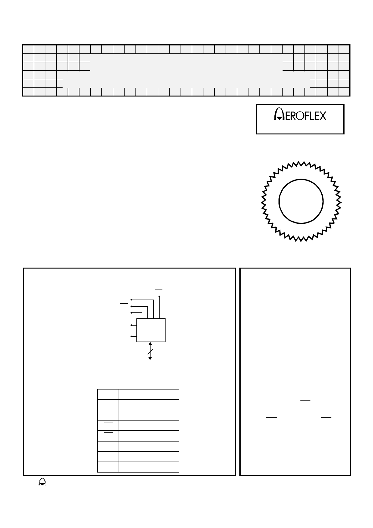
512Kx8
OE
A0 – A18
I/O0-7
8
WE
CE
Pin Description
I/O
0-7 Data I/O
A
0–18 Address Inputs
WE
Write Enable
CE
Chip Enable
OE
Output Enable
V
CC Power Supply
V
SS Ground
NC Not Connected
Vss
Vcc
Block Diagram – SOJ (L2)
Plastic Path™ Features
■ Low Power Monolithic CMOS 512K x 8 SRAM
■ Operating Temperature Range
● Full Military (-55°C to +125°C)
● Industrial (-40°C to +85°C)
■ Burn-in and Temperature Cycle Available
■ 10, 12, 15, 17, 20 & 25ns Access Times
■ +5V Power Supply
■ Industry Standard Pinouts
● Center Power / Ground Pins
■ TTL Compatible I/O
■ 3.3V Device I/O Interfacing
■ JEDEC Standard 36 pin Plastic SOJ Package
● 36 Lead, .93" x .405" x 0.148 Small Outline J lead (SOJ),
Aeroflex code# "L2"
■ Fully Static Operation
● No Clocks or Refresh Required
4 Megabit Plastic Monolithic SRAM
ACT-PS512K8 High Speed
F
I
E
I
D
C
E
R
T
A
E
R
O
F
L
E
X
L
A
B
S
I
N
C
.
ISO
900
1
Page 2
Aeroflex Circuit Technology SCD3764 REV A 6/2/98 Plainview NY (516) 694-6700
2
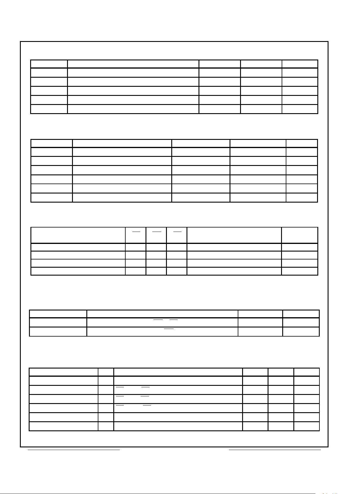
Absolute Maximum Ratings
Symbol Parameter MINIMUM MAXIMUM Units
T
C
Case Operating Temperature
-55 +125 °C
T
STG
Storage Temperature
-65 +150 °C
P
D
Maximum Package Power Dissipation
1.0 W
V
G
Maximum Signal Voltage to Ground
-0.5 V
CC
+ 0.5 V
V
CC
Power Supply Voltage
-0.5 +7.0 V
Recommended Operating Conditions
Symbol Parameter Minimum Maximum Units
V
CC
Power Supply Voltage
+4.5 +5.5 V
V
SS
Ground
0 0 V
V
IH
Input High Voltage
+2.2 V
CC
+ 0.5 V
V
IL
Input Low Voltage
-0.5 +0.8 V
T
C
Operating Temperature (Military)
-55 +125 °C
T
C
Operating Temperature (Industrial)
-40 +85 °C
Truth Table
Mode CE WE OE Data I/O
Supply
Current
Standby H X X High Z I
SB
Output Disable L H H High Z I
CC
Read L H L Data OUT I
CC
Write L L X Data IN I
CC
Capacitance
(VIN & V
OUT
= 0V, f = 1MHz, TC = 25°C, unless otherwise noted, Guaranteed but not tested)
Symbol Parameter Maximum Units
C
IN
Input Capacitance (A
0-18
, WE & OE)
6 pF
C
OUT
Output Capacitance (I/O
0-7
& CE)
8 pF
DC Characteristics
(VCC = 5.0V, VSS = 0V, TC = -55°C to +125°C or -40°C to +85°C)
Parameter Sym Conditions Min Max Units
Input Leakage Current
I
LI
VCC = Max, VIN=VSStoV
CC
-10 +10 µA
Output Leakage Current
I
LO
CE = VIH, OE = VIH, V
OUT
= VSStoV
CC
-10 +10 µA
Operating Supply Current
I
CC
CE = VIL, OE = VIH,f=5MHz,Vcc=5.5V
130 mA
Standby Current
I
SB
CE = VIH, OE= VIH, f=5MHz,Vcc=5.5V
20 mA
Output Low Voltage
V
OL
IOL = 8 mA, Vcc = 4.5V
0.4 V
Output High Voltage
V
OH
IOH = -4 mA, Vcc = 4.5V
2.4 V
Note: DC Test conditions: VIL = 0.3V, VIH = Vcc - 0.3V.
Page 3

Aeroflex Circuit Technology SCD3764 REV A 6/2/98 Plainview NY (516) 694-6700
3
AC Characteristics
(VCC = 5.0V, VSS= 0V, TC = -55°C to +125°C or -40°C to +85°C)
Read Cycle
Parameter
Sym
–010
Min Max
–012
Min Max
–015
Min Max
–017
Min Max
–020
Min Max
–025
Min Max
Units
Read Cycle Time
t
RC
10 12 15 17 20 25 ns
Address Access Time
t
AA
10 12 15 17 20 25
ns
Chip Enable Access Time
t
ACE
10 12 15 17 20 25
ns
Output Hold from Address Change
t
OH
3 3 3 3 4 5 ns
Output Enable to Output Valid
t
OE
5 6 7 8 10 12
ns
Chip Enable to Output in Low Z (1)
t
CLZ
3 3 3 3 3 3
ns
Output Enable to Output in Low Z (1)
t
OLZ
0 0 0 0 0 0 ns
Chip Deselect to Output in High Z (1)
t
CHZ
5 6 7 7 8 10
ns
Output Disable to Output in High Z (1)
t
OHZ
5 6 7 7 8 10
ns
Note 1. Guaranteed by design, but not tested
Write Cycle
Parameter
Sym
–010
Min Max
–012
Min Max
–015
Min Max
–017
Min Max
–020
Min Max
–025
Min Max
Units
Write Cycle Time
t
WC
10 12 15 17 20 25 ns
Chip Enable to End of Write
t
CW
7 8 10 12 13 15 ns
Address Valid to End of Write
t
AW
7 8 10 12 13 15 ns
Data Valid to End of Write
t
DW
5 6 8 8 9 10 ns
Write Pulse Width
t
WP
7 8 10 12 13 15 ns
Address Setup Time
t
AS
0 0 0 0 0 0 ns
Address Hold Time
t
AH
0 0 0 0 0 0 ns
Output Active from End of Write (1)
t
OW
3 3 3 3 4 5 ns
Write to Output in High Z (1)
t
WHZ
5 6 7 8 8 10 ns
Data Hold from Write Time
t
DH
0 0 0 0 0 0 ns
Note 1. Guaranteed by design, but not tested
Data Retention Electrical Characteristics (Special Order Only)
VCC = 5.0V, VSS= 0V, TC = -55°C to +125°C or -40°C to +85°C)
Parameter Sym Test Conditions
All Speeds
Min Typ Max
Units
V
CC
for Data Retention
V
DR
CE ≥ V
CC
– 0.2V
2 5.5 V
Data Retention Current
I
CCDR1
V
CC
= 3V
0.5 2.0 mA
Page 4

Aeroflex Circuit Technology SCD3764 REV A 6/2/98 Plainview NY (516) 694-6700
4
Timing Diagrams — SRAM
DI/O
tRC
tOH
tAA
Data ValidPrevious Data Valid
t
OE
High Z
t
OHZ
Read Cycle Timing Diagrams
Data Valid
tCLZ
SCE
OE
tACE
tCHZ
UNDEFINED
DON’T CARE
Read Cycle 2 (SWE = VIH)
Write Cycle (SCE
Controlled, OE = VIH )
tCW
tAS tWP
tDW
tOW
SCE
SWE
Data Valid
Write Cycle (SWE Controlled, OE = VIH)
DI/O
AC Test Circuit
IOL
Parameter Typical Units
Input Pulse Level 0 – 3.0 V
Input Rise and Fall 5 ns
Input and Output Timing Reference Level 1.5 V
Notes:
1) V
Z is programmable from -2V to +7V. 2) IOL and IOH programmable from 0 to 16 mA. 3) Tester Impedance
Z
O =75Ω. 4) VZ is typically the midpoint of VOH and VOL. 5) IOL and IOH are adjusted to simulate a typical resistance
load circuit. 6) ATE Tester includes jig capacitance.
IOH
To Device Under Test
V
Z ~ 1.5 V (Bipolar Supply)
Current Source
Current Source
C
L = 50 pF
tWC
tAW tAH
tRC
tAA
tOLZ
SEE NOTE
SEE NOTE
SEE NOTE
SEE NOTE
Note: Guaranteed by design, but not tested.
DI/O
tDH
tWHZ
SEE NOTE
Read Cycle 1 (SCE = OE = VIL, SWE = VIH)
Write Cycle Timing Diagrams
tWP
tDW
Data Valid
tWC
tAW
tAH
DI/O
tDH
SCE
SWE
tCW
tAS
A0-18
A0-18
A0-18
A0-18
AC Test Conditions
Page 5

Aeroflex Circuit Technology SCD3764 REV A 6/2/98 Plainview NY (516) 694-6700
5
Pin Numbers & Functions
36 Pins — SOJ
Pin # Function Pin # Function
1 A
0 19 NC
2 A
1 20 A10
3 A2 21 A11
4 A3 22 A12
5 A4 23 A13
6 CE 24 A14
7 I/O0 25 I/O4
8 I/O1 26 I/O5
9 VCC 27 VCC
10 VSS 28 VSS
11 I/O2 29 I/O6
12 I/O3 30 I/O7
13 WE 31 OE
14 A5 32 A15
15 A6 33 A16
16 A7 34 A17
17 A8 35 A18
18 A9 36 NC
All dimensions in inches
Dimensions in inches (.xxx)
Package Outline "L2" — SOJ Package, 36 Leads
11.30 (.445)
11.05 (.435)
9.65 (.380)
9.14 (.360)
.69
(.027)
23.62 (.930)
23.37 (.920)
10.29 (.405)
10.03 (.395)
0.95
(.037)
1.27
(.050)
.43
(.017
3.76 (.148) MAX
Dimensions in millmeters mm
1 18
1936
MIN
TYP
+.10
-.05
+.004)
-.002)
TYP
.004 MAX
Page 6

Aeroflex Circuit Technology SCD3764 REV A 6/2/98 Plainview NY (516) 694-6700
6
Ordering Information (Typical)
Model Number Options Speed Package
ACT-PS512K8N–010L2I None 10ns 36 Lead SOJ
ACT-PS512K8W–012L2I Burn-in 12ns 36 Lead SOJ
ACT-PS512K8X–015L2T Temp Cycle 15ns 36 Lead SOJ
ACT-PS512K8Y–017L2T Temp Cycle & Burn-in 17ns 36 Lead SOJ
ACT-PS512K8Y–020L2T Temp Cycle & Burn-in 20ns 36 Lead SOJ
ACT-PS512K8Y–025L2T Temp Cycle & Burn-in 25ns 36 Lead SOJ
010 = 10ns
012 = 12ns
015 = 15ns
017 = 17ns
020 = 20ns
025 = 25ns
Aeroflex Circuit
Technology
* Screened to the test methods of MIL-STD-883
Aeroflex Circuit Technology
35 South Service Road
Plainview New York 11830
Telephone: (516) 694-6700
FAX: (516) 694-6715
Toll Free Inquiries: 1-(800) 843-1553
CIRCUIT TECHNOLOGY
\\\
ACT- P S 512K 8 N– 010 L2 T
Memory Type
S = Plastic SRAM
Memory Depth, Locations
Options
Memory Width, Bits
N = None
W = Burn-in
*
X = Temperature Cycle *
Y = Burn-in & Temperature Cycle *
Memory Speed, ns
Package Type & Size
L2 = 36 Pin Plastic SOJ
Electrical Testing
I = Industrial Temp, -40°C to +85°C
T = Military Temp, -55°C to +125°C
Plastic Path
Part Number Breakdown
 Loading...