

Datasheet ACT-F4M32C-100F2M, ACT-F4M32C-100F2I, ACT-F4M32C-100F2C, ACT-F4M32C-100F1M, ACT-F4M32C-100F1I Datasheet (ACT)
...Page 1
ACT–F4M32A High Speed 128 Megabit
Sector Erase
FLASH Multichip Module
Advanced
CIRCUIT TECHNOLOGY
Features
■ 8 Low Voltage/Power AMD 2M x 8 FLASH Die in One
MCM Package
■ Overall Configuration is 4M x 32
■ +5V Power Supply / +5V Programing Operation
■ Access Times of 100, 120 and 150 ns
■ Erase/Program Cycles – 100,000 Minimum (+25°C)
■ Sector erase architecture (Each Die)
● 32 uniform sectors of 64 Kbytes each
● Any combination of sectors can be erased. Also
supports full chip erase
● Sector group protection is user definable
Embedded Erase Algorithims – Automatically
■
pre-programs and erases the die or any sector
■ Embedded Program Algorithims – Automatically
programs and verifies data at specified address
www.aeroflex.com/act1.htm
■ Ready/Busy output (RY/BY) – Hardware method for
detection of program or erase cycle completion
■ Hardware RESET pin – Resets internal state machine
to the read mode
■ Erase Suspend/Resume – Supports reading or
programming data to a sector not being erased
■ Packaging – Hermetic Ceramic
● 68–Lead, Low Profile CQFP(F1), 1.56"SQ x .140"max
● 68–Lead, Dual-Cavity CQFP(F2), 0.88"SQ x .20"max
(.18 max thickness available, contact factory for details)
(Drops into the 68 Lead JEDEC .99"SQ CQFJ footprint)
Internal Decoupling Capacitors for Low Noise
■
Operation
■ Commercial, Industrial and Military Temperature
Ranges
■ MIL-PRF-38534 Compliant MCMs Available
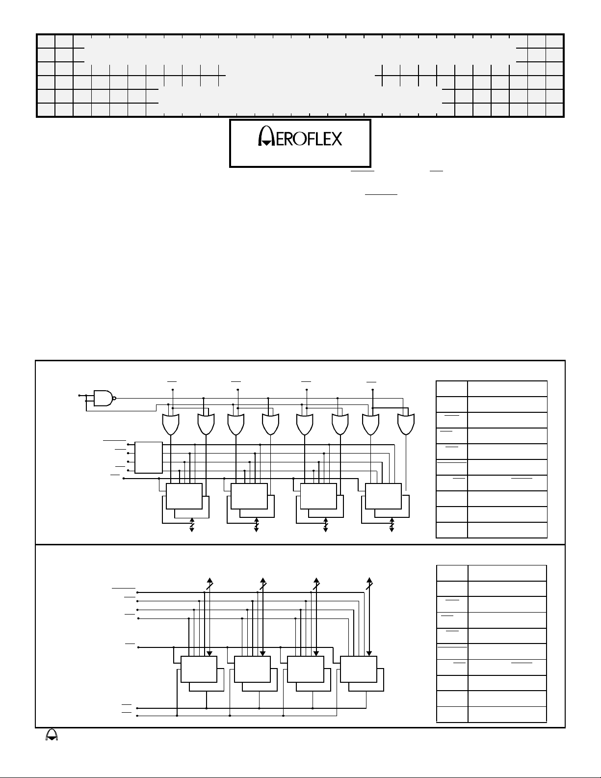
Block Diagram – CQFP(F1)
A21
RESET
WE
A0 - A20
OE
RY/BY
CE1
Buffer
2Mx8
2Mx8
Block Diagram – CQFP(F2)
RESET
WE
A0 - A 20
OE
RY/BY
2Mx8
1
CE
CE2
2 CE3
CE
2Mx8
2Mx8
I/O8-15 I/O16-23I/O0-7 I/O24-31
I/O8-15 I/O16-23I/O0-7 I/O24-31
8 88 8
2Mx8
2Mx8
2Mx8
2Mx8
2Mx8
2Mx8
2Mx8
2Mx8
2Mx8
CE4
2Mx8
2Mx8
Pin Description
0-31 Data I/O
I/O
0–21 Address Inputs
A
WE
CE
OE
RESET
RY/BY
Write Enables
1-4 Chip Enables
Output Enable
Reset
Ready/Busy
VCC Power Supply
GND Ground
8888
NC Not Connected
Pin Description
0-31 Data I/O
I/O
0–20 Address Inputs
A
WE
CE
OE
RESET
RY/BY
Write Enable
1,2 Chip Enables
Output Enable
Reset
Ready/Busy
VCC Power Supply
GND Ground
NC Not Connected
eroflex Circuit Technology - Advanced Multichip Modules © SCD3866 REV 1 12/4/98
Page 2
General Description
Utilizing AMD’s Sector Erase Flash Memory Die, the ACT-F4M32A is a high speed, 128
megabit CMOS flash multichip module (MCM) designed for full temperature range, military,
space, or high reliability applications.
The ACT-F4M32A consists of eight high-performance AMD Am29F016 16Mbit
(16,777,216 bit) memory die. Each die contains 8 separately write or erase sector groups
of 256Kbytes (A sector group consists of 4 adjacent sectors of 64Kbytes each).
The command register is written by bringing WE
low and OE
(OE
) being logically active. Access time grades of 100ns, 120ns and 150ns maximum are
is high (VIH). Reading is accomplished by chip Enable (CE) and Output Enable
to a logic low level (VIL), while CE is
standard.
The ACT-F4M32A is offered in two different hermetically sealed co-fired 68 lead
ceramic packages. This allows operation in a military environment temperature range of
-55°C to +125°C.
The ACT-F4M32A can be programmed (both read and write functions) in-system using
the +5.0V V
operations. The end of program or erase is detected by the RY/BY
CC power supply. A 12.0V VPP is not required for programming or erase
pin, Data Polling of
DQ7, or by the Toggle bit (DQ6).
The ACT-F4M32A also has a hardware RESET
pin. When this pin is driven low,
execution of any Embedded Program Alggorithm or Embedded Erase Algorithm will be
terminated.
Each block can be independently erased and programmed 100,000 times at +25°C.
For Detail Information regarding the operation of the Am29F016 Sector Erase Flash
Memory, see the AMD datasheet (Publication 18805).
Aeroflex Circuit Technology SCD3866 REV 1 12/4/98 Plainview NY (516) 694-67002
Page 3

Pin Numbers & Functions
68 Pins — CQFP
Pin # Function Pin # Function Pin # Function Pin # Function
1 GND 18 GND 35 OE
2 CE
1 19 I/O8 36 CE4 53 I/O23
3 A5 20 I/O9 37 A17 54 I/O22
4 A4 21 I/O10 38 A18 55 I/O21
5 A3 22 I/O11 39 A19 56 I/O20
6 A2 23 I/O12 40 A20 57 I/O19
7 A1 24 I/O13 41 A21 58 I/O18
8 A0 25 I/O14 42 RESET 59 I/O17
9 RY/BY 26 I/O15 43 NC 60 I/O16
10 I/O0 27 VCC 44 I/O31 61 VCC
11 I/O1 28 A11 45 I/O30 62 A10
12 I/O2 29 A12 46 I/O29 63 A9
13 I/O3 30 A13 47 I/O28 64 A8
14 I/O4 31 A14 48 I/O27 65 A7
15 I/O5 32 A15 49 I/O26 66 A6
16 I/O6 33 A16 50 I/O25 67 WE
17 I/O7 34 CE2 51 I/O24 68 CE3
Consult Factory for Special order: Pin 9 -NC
52 GND
Package Outline — CQFP "F1"
Pin 1
Pin 10
Pin 26
.015 ±.003
.800
(16 at .050 4 sides)
REF
.200 REF
Pin 61Pin 9
Pin 60
Pin 44
Pin 43Pin 27
.480 MIN
(4 Sides)
1.575 SQ
MAX
1.50
(4 Sides)
.010
±.002
All dimensions in inches
.140
MAX
.050 ±.005
.060 REF
Aeroflex Circuit Technology SCD3866 REV 1 12/4/98 Plainview NY (516) 694-67003
Page 4

Pin Numbers & Functions
68 Pins — Dual-Cavity CQFP
(Standard Configuration)
Pin # Function Pin # Function Pin # Function Pin # Function
1 GND 18 GND 35 OE
2 NC 19 I/O
8 36 CE2 53 I/O23
52 GND
3 A5 20 I/O9 37 A17 54 I/O22
4 A4 21 I/O10 38 RY/BY 55 I/O21
5 A3 22 I/O11 39 NC 56 I/O20
6 A2 23 I/O12 40 NC 57 I/O19
7 A1 24 I/O13 41 A18 58 I/O18
8 A0 25 I/O14 42 A19 59 I/O17
9 RESET 26 I/O15 43 A20 60 I/O16
10 I/O0 27 VC C 44 I/O31 61 VCC
11 I/O1 28 A11 45 I/O30 62 A10
12 I/O2 29 A12 46 I/O29 63 A9
13 I/O3 30 A13 47 I/O28 64 A8
14 I/O4 31 A14 48 I/O27 65 A7
15 I/O5 32 A15 49 I/O26 66 A6
16 I/O6 33 A16 50 I/O25 67 WE
17 I/O7 34 CE1 51 I/O24 68 NC
Consult Factory for Special order: Pin 38 -NC
Package Outline — Dual-Cavity CQFP "F2"
Top View
.990 SQ
±.010
.890 SQ
Pin 9 Pin 61
Pin 10
Pin 26
MAX
.800 REF
Pin 60
Pin 44
Pin 43Pin 27
.015
±.002
.050
TYP
*.200 MAX
+3°/-3°
.040
±.005
See Detail “A”
.010 ±.002
.010 R
REF
Detail “A”
.010 REF
.010 REF
.010 ±.005
All dimensions in inches
Aeroflex Circuit Technology SCD3866 REV 1 12/4/98 Plainview NY (516) 694-67004
*.180 MAX available, call factory for details
Page 5

Ordering Information
CIRCUIT TECHNOLOGY
Model Number Screening Speed Package
ACT–F4M32C–100F1C Commercial (0°C to +70°C)
ACT–F4M32A–100F2C Commercial (0°C to +70°C)
ACT–F4M32C–100F2C Commercial (0°C to +70°C)
ACT–F4M32A–100F1C Commercial (0°C to +70°C)
ACT–F4M32C–100F1I Industrial (-40°C to +85°C)
ACT–F4M32A–100F2I Industrial (-40°C to +85°C)
ACT–F4M32C–100F2I Industrial (-40°C to +85°C)
ACT–F4M32A–100F1I Industrial (-40°C to +85°C)
ACT–F4M32C–100F1M Military (-55°C to +125°C)
ACT–F4M32A–100F2M Military (-55°C to +125°C)
ACT–F4M32C–100F2M Military (-55°C to +125°C)
ACT–F4M32A–100F1M Military (-55°C to +125°C)
Part Number Breakdown
ACT– F 4M 32 A– 100 F1 M
Aeroflex Circuit
Technology
Memory Type
S = SRAM
F = FLASH EEPROM
E = EEPROM
D = Dynamic RAM
Memory Depth, Locations
Memory Width, Bits
Pinout Options
F2 - A = One WE, RY/BY access on Pin 38 - Standard pinout
F2 - C = RY/BY
F1 - A = One WE
F1 - C = RY/BY
Memory Speed, ns (+5V VCC)
internally tied - Optional pinout
, RY/BY access on Pin 9 - Standard pinout
internally tied - Optional pinout
C = Commercial Temp, 0°C to +70°C
I = Industrial Temp, -40°C to +85°C
T = Military Temp, -55°C to +125°C
M = Military Temp, -55°C to +125°C, Screened
Q = MIL-PRF-38534 Compliant/SMD if applicable
F1 = 1.56"SQ 68 Pin CQFP
F2 = .88"SQ 68 Pin Dual-Cavity CQFP
* Screened to the individual test methods of MIL-STD-883
100 ns
100 ns
100 ns
100 ns
100 ns
100 ns
100 ns
100 ns
100 ns
100 ns
100 ns
100 ns
Screening
Package Type & Size
Surface Mount Packages
1.56"sq CQFP
.88"sq CQFP
.88"sq CQFP
1.56"sq CQFP
1.56"sq CQFP
.88"sq CQFP
.88"sq CQFP
1.56"sq CQFP
1.56"sq CQFP
.88"sq CQFP
.88"sq CQFP
1.56"sq CQFP
*
Specifications subject to change without notice
Aeroflex Circuit Technology
35 South Service Road
Plainview New York 11803
www.aeroflex.com/act1.htm
Aeroflex Circuit Technology SCD3866 REV 1 12/4/98 Plainview NY (516) 694-67005
Telephone: (516) 694-6700
FAX: (516) 694-6715
Toll Free Inquiries: (800) 843-1553
E-Mail: sales-act@aeroflex.com
 Loading...