

Datasheet ACT-F2M32A-150F18Q, ACT-F2M32A-150F18M, ACT-F2M32A-150F18I, ACT-F2M32A-150F18C, ACT-F2M32A-120F18Q Datasheet (ACT)
...Page 1
ACT–F2M32A High Speed 64 Megabit
Sector Erase
FLASH Multichip Module
CIRCUIT TECHNOLOGY
Features
■ 4 Low Voltage/Power AMD 2M x 8 FLASH Die in One
MCM Package
■ Overall Configuration is 2M x 32
■ +5V Power Supply / +5V Programing Operation
■ Access Times of 90, 120 and 150 ns
■ Erase/Program Cycles – 100,000 Minimum
■ Sector erase architecture (Each Die)
● 32 uniform sectors of 64 Kbytes each
● Any combination of sectors can be erased. Also
supports full chip erase
● Sector group protection is user definable
■ Embedded Erase Algorithims – Automatically
pre-programs and erases the die or any sector
■ Embedded Program Algorithims – Automatically
programs and verifies data at specified address
www.aeroflex.com/act1.htm
■ Ready/Busy output (RY/BY) – Hardware method for
detection of program or erase cycle completion
■ Hardware RESET pin – Resets internal state machine
to the read mode
■ Erase Suspend/Resume – Supports reading or
programming data to a sector not being erased
■ Packaging – Hermetic Ceramic
● 68 Lead, .94" x .94" x .140" Single-Cavity Small
Outline Gull Wing, Aeroflex code# "F18" (Drops into
the 68 Lead JEDEC .99"SQ CQFJ footprint)
■ Internal Decoupling Capacitors for Low Noise
Operation
■ Commercial, Industrial and Military Temperature
Ranges
■ MIL-PRF-38534 Compliant MCMs Available
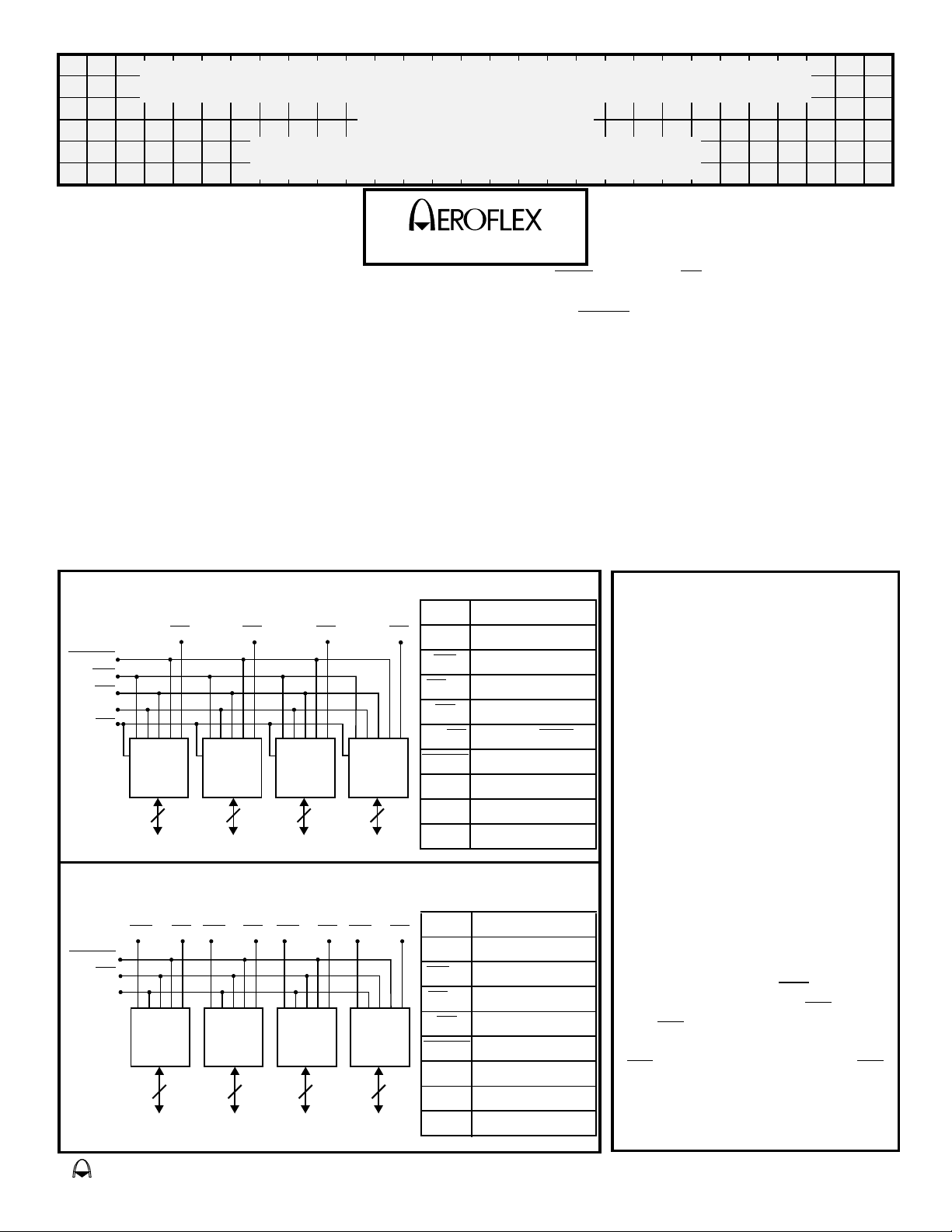
Block Diagram – CQFP(F18)
Standard Configuration
CE1 CE2
RESET
WE
OE
A0 – A20
RY/BY
2Mx8 2Mx8 2Mx8 2Mx8
8 8
I/O0-7 I/O8-15 I/O16-23 I/O24-31
8
Block Diagram – CQFP(F18)
Optional Configuration
RESET
OE
A0 – A20
2Mx8 2Mx8 2Mx8 2Mx8
8 8 8 8
I/O0-7 I/O8-15 I/O16-23 I/O24-31
CE
CE3 WE4WE3WE2WE1 CE1 CE2
Pin Description
I/O
0-31 Data I/O
3
CE4
A
0–20 Address Inputs
WE
CE
OE
RY/BY
RESET Reset
V
8
GND Ground
NC Not Connected
Write Enables
1-4 Chip Enables
Output Enable
Ready/Busy
CC Power Supply
General Description
Utilizing AMD’s Sector Erase
Flash Memory Die, the
ACT-F2M32A is a high speed,
64 megabit CMOS flash
multichip module (MCM)
designed for full temperature
range, military, space, or high
reliability applications.
The ACT-F2M32A consists of
four high-performance AMD
Am29F016 16Mbit (16,777,216
bit) memory die. Each die
contains 8 separately write or
Pin Description
erase sector groups of
256Kbytes (A sector group
I/O
CE4
0-31 Data I/O
A
0–20 Address Inputs
WE
1-4 Write Enable
CE
1-4 Chip Enables
OE
RESET
V
CC Power Supply
GND Ground
NC Not Connected
Output Enable
Reset
consists of 4 adjacent sectors of
64Kbytes each).
The command register is
written by bringing WE
low level (V
and OE
IL), while CE is low
is high (VIH). Reading is
to a logic
accomplished by chip Enable
) and Output Enable (OE)
(CE
being logically active. Access
time grades of 90ns, 120ns and
150ns maximum are standard.
eroflex Circuit Technology - Advanced Multichip Modules © SCD1666A REV A 9/12/97
Page 2

General Description, Cont’d,
The ACT-F2M32A is packaged in a hermetically sealed co-fired ceramic 68 lead, .94"
SQ Ceramic Gull Wing CQFP package. This allows operation in a military environment
temperature range of -55°C to +125°C.
The ACT-F2M32A can be programmed (both read and write functions) in-system using
the +5.0V V
operations. The end of program or erase is detected by the RY/BY
DQ7, or by the Toggle bit (DQ6).
CC power supply. A 12.0V VPP is not required for programming or erase
pin, Data Polling of
The ACT-F2M32A also has a hardware RESET
pin. When this pin is driven low,
execution of any Embedded Program Alggorithm or Embedded Erase Algorithm will be
terminated.
Each block can be independently erased and programmed 100,000 times at +25°C.
For Detail Information regarding the operation of the Am29F016 Sector Erase Flash
Memory, see the AMD datasheet (Publication 18805).
Aeroflex Circuit Technology SCD1666A REV A 9/12/97 Plainview NY (516) 694-6700
2
Page 3
Absolute Maximum Ratings
Parameter Range Units
Case Operating Temperature Range
Storage Temperature Range
(1)
Voltage with Respect to GND (All pins except A
Voltage on Pins A
9, OE, RESET
(2)
Vcc Supply Voltage with Respect to Ground
Output Short Circuit Current
Notes:
1. Minimum DC voltage is -0.5V on input/output pins. During Transitions, inputs may undershoot GND to -2.0V for periods up to 20ns. Maximum DC voltage on
input/output pins is V
2. Minimum DC input voltage on A
Maximum DC input voltage on A
3. No more than one output shorted to ground for no more than 1 second.
NOTICE: Stresses above those listed under "Absolute Maximums Rating" may cause permanent damage to the device. These are stress rating only; functional
operation beyond the "Operation Conditions" is not recommended and extended exposure beyond the "Operation Conditions" may effect device reliability.
CC + 0.5V, which may overshoot to VCC + 2.0V for periods up to 20ns.
(3)
9 ,OE, RESET pins is -0.5V. During Voltage transitions, A9, OE & RESET may overshoot GND to -2.0V for periods up to 20ns.
9 is +12.5V which may overshoot to 14V for periods up to 20ns.
9)
(1)
-55 to +125 °C
-65 to +150 °C
-2.0 to +7.0 V
-2.0 to +13.5 V
-2.0 to +7.0 V
200 mA
Recommended Operating Conditions
Symbol Parameter Minimum Maximum Units
CC
V
V
V
T
5V Power Supply Voltage (10%)
IH
Input High Voltage (CMOS)
IL
Input Low Voltage
C
Operating Temperature (Military)
+4.5 +5.5 V
0.7 x V
CC V
+ 0.3 V
cc
-0.5 +0.8 V
-55 +125 °C
Capacitance
(f = 1MHz, TC = 25°C, Standard Configuration)
Symbol Parameter Maximum Units
C
C
C
RESET
C
C
RY/BY
C
C
AD
A0 – A20 Capacitance
OE
OE Capacitance
CE
CE Capacitance
RESET Capacitance
WE
WE Capacitance
RY/BY Capacitance
I/O
I/O0 – I/O31 Capacitance
50 pF
50 pF
20 pF
50 pF
60 pF
50 pF
20 pF
Capacitance Guaranteed by design, but not tested.
DC Characteristics – CMOS Compatible
(TC = -55°C to +125°C, VCC = +4.5V to + 5.5V, Unless otherwise specified)
Parameter Sym Conditions Min Max Units
CC
CC -
10 µA
50 µA
10 µA
160 mA
240 mA
4 mA
4 mA
0.45 V
V
V
Input Load Current
A9 Leakage Current
Output Leakage Current
Vcc Active Read Current
Vcc Active Program/Erase Current
Vcc Standby Current
Vcc Standby Current (Reset)
Output Low Voltage
Output High Voltage
CC Lock-Out Voltage
Low V
Notes:
1. Not 100% tested.
IL
I
VCC = VCCMax., VIN = VCC or GND
LIT
I
VCC = VCCMax., A9 = +12V
LO
I
VCC = VCCMax., VIN = GND to VCC
CC1
I
(1)
I
CC2
CC3
I
CC4
I
OL
V
OH1
V
OH2
V
V
LKO 3.2 4.2 V
= VIL, OE = VIH
CE
= VIL, OE = VIH
CE
CC = VCCMax., CE = RESET = VCC ± 0.3V
V
CC = VCCMax., RESET = VCC ± 0.3V
V
VCC = VCCMin., IOL = 12 mA
CC = VCCMin., IOH = -2.5 mA
V
CC = VCCMin., IOH = -100 µA
V
0.85 x
V
V
0.4V
Aeroflex Circuit Technology SCD1666A REV A 9/12/97 Plainview NY (516) 694-6700
3
Page 4

AC Characteristics – Write/Erase/Program Operations – WE Controlled
(TC = -55°C to +125°C, VCC = +4.5V to + 5.5V, Unless otherwise specified)
Parameter
Write Cycle Time
Address Setup to WE
Address Hold Time from CE
Data Setup to WE
Data Hold Time from WE
Going Low
High
Going High
High
Output Enable Hold Time
Read Recover Time Before Write
High to WE Low)
(OE
Setup Time from WE Low
CE
Hold Time from WE High
CE
Pulse Width
WE
Pulse Width High
WE
Byte Programming Operation
Sector Erase Operation
CC Set-Up Time
V
Rise Time to V
Setup Time to WE Active
OE
Pulse Width
Reset
Program/Erase Valid to RY/BY
ID
Delay
Notes:
1. Not 100% tested.
Read
Toggle Bit I and Data
Parameter
Symbol
Standard
WC tAVAV 90 120 150 ns
t
t
AS tAVWL 0 0 0 ns
t
AH tWLAX 45 50 50 ns
t
DS tDVWH 45 50 50 ns
t
DH tWHDX 0 0 0 ns
OEH
Polling 10 10 10 ns
t
t
GHWL tGHWL 0 0 0 ns
t
CS tELWL 0 0 0 ns
t
CH tWHEH 0 0 0 ns
t
WP tWLWH 45 50 50 ns
t
WPH tWHWL 20 20 20 ns
WHWH1 tWHWH1 8 8 8 µs
t
WHWH2 tWHWH2 15 15 15 Sec
t
t
VCS 50 50 50 µs
Parameter
Symbol
JEDEC
90ns 120ns 150ns
Min Max Min Max Min Max
0 0 0 ns
Units
tVIDR 500 500 500 ns
tOESP 4 4 4 µs
tRP 500 500 500 ns
tBUSY 40 50 60 ns
Parameter
Read Cycle Time
(1)
Address to Output Delay
to Output Delay
CE
to Output Delay
OE
to Output in High Z
CE
to Output in High Z
OE
(1)
(1)
Output Hold from Addresses, CE
First
Low to Read Mode
RESET
Notes:
1. Not 100% tested.
(1)
AC Characteristics – Read Only Operations
(TC = -55°C to +125°C, VCC = +4.5V to + 5.5V, Unless otherwise specified)
or OE Change, Whichever Occurs
Parameter
Symbol
Standard
tRC tAVAV 90 120 150 ns
ACC tAVQV 90 120 150 ns
t
t
CE tELQV 90 120 150 ns
t
OE tGLQV 40 50 55 ns
tDF tEHQZ 20 30 35 ns
tDF tGHQZ 20 0 30 0 35 ns
OH tAXQX 0 0 0 ns
t
tREADY 20 20 20 µs
Parameter
Symbol
JEDEC
90ns 120ns 150ns
Min Max Min Max Min Max
Units
Aeroflex Circuit Technology SCD1666A REV A 9/12/97 Plainview NY (516) 694-6700
4
Page 5

AC Characteristics – Write/Erase/Program Operations – CE Controlled
(TC = -55°C to +125°C, VCC = +4.5V to + 5.5V, Unless otherwise specified)
Parameter
Write Cycle Time
Address Setup to CE
Address Hold Time from CE
Data Setup to CE
Data Hold Time from CE
Output Enable Setup Time
Output Enable Hold Time
(1)
Going Low
Low
Going High
High
(1)
(1)
Read Recover Time Before Write
High to WE Low)
(OE
Setup Time from WE Low
CE
Hold Time from CE High
WE
Pulse Width
WE
Pulse Width High
WE
Byte Programming Operation
Sector Erase Operation
Notes:
1. Not 100% tested.
Read
Toggle Bit I and Data
Parameter
Symbol
Standard
Parameter
Symbol
JEDEC
90ns 120ns 150ns
Min Max Min Max Min Max
Units
tWC tAVAV 90 120 150 ns
t
AS tAVEL 0 0 0 ns
t
AH tELAX 45 50 50 ns
t
DS tDVEH 45 50 50 ns
t
DH tEHDX 0 0 0 ns
tOES 0 0 0 ns
OEH
Polling 10 10 10 ns
t
t
GHEL tGHEL 0 0 0 ns
t
WS tWLEL 0 0 0 ns
t
WH tEHWH 0 0 0 ns
t
CP tELEH 45 50 50 ns
t
CPH tELEL 20 20 20 ns
WHWH1 tWHWH1 8 8 8 µs
t
WHWH2 tWHWH2 15 15 15 Sec
t
0 0 0 ns
Aeroflex Circuit Technology SCD1666A REV A 9/12/97 Plainview NY (516) 694-6700
5
Page 6

Device
Under
Test
AC Test Circuit
Test Configuration Component Values
C
Test Configuration
CC
V
R1
OUT
C
L
R2
3.3V Standard Test 50 990 770
5V Standard Test 50 580 390
NOTES:
C
L includes jig capacitance.
L
(pF)
Parameter Typical Units
Input Pulse Level 0 – 3.0 V
Input Rise and Fall 5 ns
Input and Output Timing Reference Level 1.5 V
R1
(Ω)
R2
(Ω)
Addresses
CE
OE
WE
Data
+5 Volt
AC Waveforms for Write and Erase Operations, WE Controlled
3rd Bus Cycle
5555H PA PA
tWC
tAS
tAH
tGHWL
tWP
tCS
tWPH
tDH
AOH
PD DQ7
tDS
Data
tWHWH1
Polling
tRC
tOE
DOUT
tCE
tDF
tOH
Aeroflex Circuit Technology SCD1666A REV A 9/12/97 Plainview NY (516) 694-6700
6
Page 7

AC Waveforms for Write and Erase Operations, CE Controlled
Data
Polling
Addresses
WE
OE
CE
Data
+5 Volt
5555H PA PA
tWC
tGHEL
tWS
AOH
tDS
tAS
tCP
tCPH
tAH
tWHWH1
tDH
PD DQ7
AC Waveform For Read Operations
DOUT
Addresses
CE
OE
WE
Outputs
tRC
Addresses Stable
tACC
tOE
tOEH
tCE
tOH
High Z High Z
Output Valid
tDF
Aeroflex Circuit Technology SCD1666A REV A 9/12/97 Plainview NY (516) 694-6700
7
Page 8

Pin Numbers & Functions
68 Pins — Dual-Cavity CQFP
(Standard Configuration)
Pin # Function Pin # Function Pin # Function Pin # Function
1 GND 18 GND 35 OE
2 CE
3 19 I/O8 36 CE2 53 I/O23
52 GND
3 A5 20 I/O9 37 A17 54 I/O22
4 A4 21 I/O10 38 RY/ BY 55 I/O21
5 A3 22 I/O11 39 NC 56 I/O20
6 A2 23 I/O12 40 NC 57 I/O19
7 A1 24 I/O13 41 A18 58 I/O18
8 A0 25 I/O14 42 A19 59 I/O17
9 RESET 26 I/O15 43 A20 60 I/O16
10 I/O0 27 VCC 44 I/O31 61 VCC
11 I/O1 28 A11 45 I/O30 62 A10
12 I/O2 29 A12 46 I/O29 63 A9
13 I/O3 30 A13 47 I/O28 64 A8
14 I/O4 31 A14 48 I/O27 65 A7
15 I/O5 32 A15 49 I/O26 66 A6
16 I/O6 33 A16 50 I/O25 67 WE
17 I/O7 34 CE1 51 I/O24 68 CE4
Consult Factory for Special order (Optional Configuration): Pin 38 - WE2, Pin 39 - WE3, Pin 40 - WE4 and Pin 67 - WE1
"F18" — CQFP Package
.990 SQ
±.010
.940 SQ
Pin 9
Pin 10
Pin 26
±.009
.800 REF
Pin 61
Pin 60
Pin 44
Pin 43Pin 27
.015
±.002
.900 SQ
REF
.140
MAX
.640 SQ
REF
.008
±.002
.040
Detail “A”
Metal spacer
.010
±.008
.015
±.002
See Detail “A”
All dimensions in inches
Aeroflex Circuit Technology SCD1666A REV A 9/12/97 Plainview NY (516) 694-6700
8
Page 9

Ordering Information
CIRCUIT TECHNOLOGY
Memory Speed, ns (+5V V
Model Number Screening Speed Package
ACT–F2M32A–090F18C Commercial (0°C to +70°C)
ACT–F2M32A–120F18C Commercial (0°C to +70°C)
ACT–F2M32A–150F18C Commercial (0°C to +70°C)
ACT–F2M32A–090F18I Industrial (-40°C to +85°C)
ACT–F2M32A–120F18I Industrial (-40°C to +85°C)
ACT–F2M32A–150F18I Industrial (-40°C to +85°C)
ACT–F2M32A–090F18M Military (-55°C to +125°C)
ACT–F2M32A–120F18M Military (-55°C to +125°C)
ACT–F2M32A–150F18M Military (-55°C to +125°C)
ACT–F2M32A–090F18Q DESC Drawing Pending
MIL-PRF-38534 Compliant
ACT–F2M32A–120F18Q DESC Drawing Pending
MIL-PRF-38534 Compliant
ACT–F2M32A–150F18Q DESC Drawing Pending
MIL-PRF-38534 Compliant
Part Number Breakdown
90 ns
120 ns
150 ns
90 ns
120 ns
150 ns
90 ns
120 ns
150 ns
90 ns
120 ns
150 ns
CQFP
CQFP
CQFP
CQFP
CQFP
CQFP
CQFP
CQFP
CQFP
CQFP
CQFP
CQFP
ACT– F 2M 32 A– 090 F18 M
Aeroflex Circuit
Technology
Memory Type
S = SRAM
F = FLASH EEPROM
E = EEPROM
D = Dynamic RAM
Memory Depth, Locations
Memory Width, Bits
Pinout Options
A = One WE, RY/BY access on Pin 38 - Standard pinout
C = Four WE’s & RY/BY internally tied - Optional pinout
CC)
Specifications subject to change without notice
Aeroflex Circuit Technology
35 South Service Road
Plainview New York 11830
www.aeroflex.com/act1.htm
Aeroflex Circuit Technology SCD1666A REV A 9/12/97 Plainview NY (516) 694-6700
9
C = Commercial Temp, 0°C to +70°C
I = Industrial Temp, -40°C to +85°C
T = Military Temp, -55°C to +125°C
M = Military Temp, -55°C to +125°C, Screened
Q = MIL-PRF-38534 Compliant/SMD if applicable
F18 = .94" SQ 68 Lead\Dual-Cavity CQFP
* Screened to the individual test methods of MIL-STD-883
Telephone: (516) 694-6700
FAX: (516) 694-6715
Toll Free Inquiries: (800) 843-1553
E-Mail: sales-act@aeroflex.com
Screening
*
Package Type & Size
Surface Mount Packages
 Loading...