

Datasheet ACT-F1M32B-120F14Q, ACT-F1M32B-120F14M, ACT-F1M32B-120F14I, ACT-F1M32B-120F14C, ACT-F1M32B-100F14Q Datasheet (ACT)
...Page 1
eroflex Circuit Technology - Advanced Multichip Modules © SCD1661B REV A 1/16/97
ACT–F1M32 High Speed 32 Megabit
Boot Block
FLASH Multichip Module
CIRCUIT TECHNOLOGY
www.aeroflex.com/act1.htm
Features
■ 4 Low Voltage/Power Intel 1M x 8 FLASH Die in One
MCM Package
■ Overall Configuration is 1M x 32
■ +5V Operation (Standard) or +3.3V (Consult Factory)
■ Access Times of 80, 100 and 120 nS ( 5V VCC)
■ +5V or +12V Programing
■ Erase/Program Cycles
● 100,000 Commercial
● 10,000 Military and Industrial
■ Sector Architecture (Each Die)
● One 16K Protected Boot Block (Bottom Boot Block
Standard, Top Boot Block Special Order)
● Two 8K Parameter Blocks
● One 96K Main Block
● Seven 128K Main Blocks
■ Single Block Erase (All bits set to 1)
■ Hardware Data Protection Feature
■ Independent Boot Block Locking
■ MIL-PRF-38534 Compliant MCMs Available
■ Packaging – Hermetic Ceramic
● 68 Lead, .94" x .94" x .180" Dual-Cavity Small
Outline Gull Wing, Aeroflex code# "F14" (Drops into
the 68 Lead JEDEC .99"SQ CQFJ footprint)
■ Internal Decoupling Capacitors for Low Noise
Operation
■ Commercial, Industrial and Military Temperature
Ranges
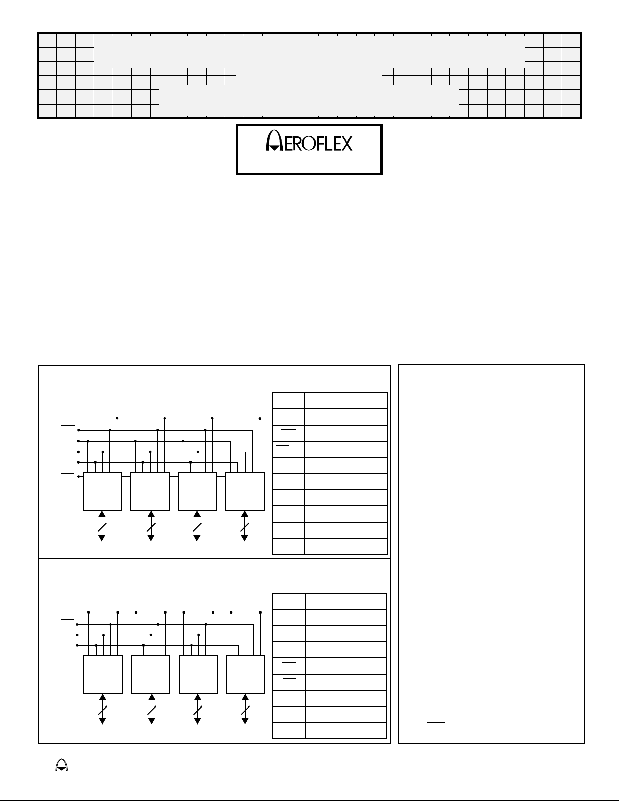
Block Diagram – CQFP(F14)
Standard Configuration
CE1 CE2
WP
WE
OE
A0 – A19
RP
1Mx8 1Mx8 1Mx8 1Mx8
8 8 8 8
I/O0-7 I/O8-15 I/O16-23 I/O24-31
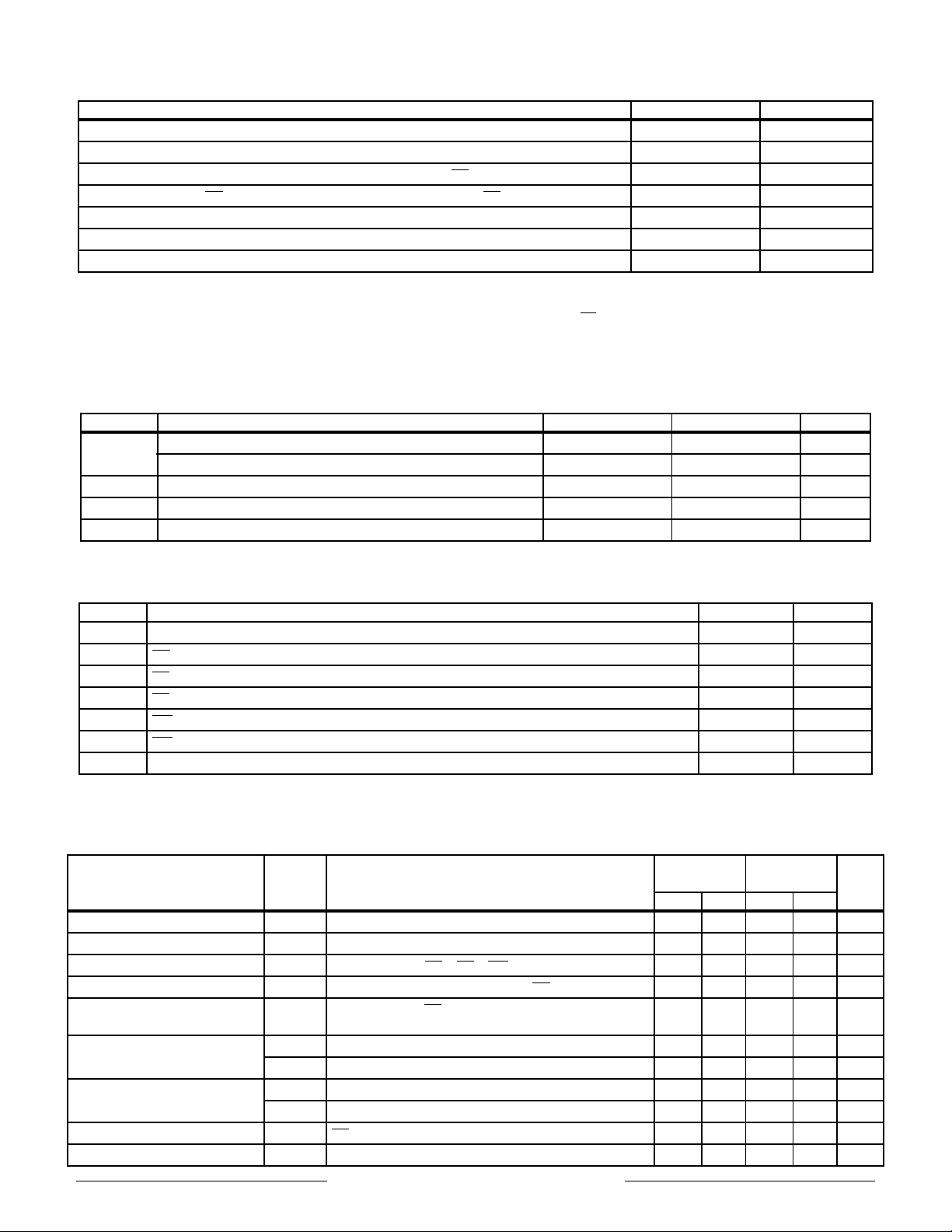
Block Diagram – CQFP(F14)
Optional Configuration
RP
OE
A0 – A19
1Mx8 1Mx8 1Mx8 1Mx8
8 8 8 8
I/O0-7 I/O8-15 I/O16-23 I/O24-31
CE
CE3 WE4WE3WE2WE1 CE1 CE2
Pin Description
0-31 Data I/O
I/O
3
CE4
0–19 Address Inputs
A
WE
1-4 Chip Enables
CE
OE
WP
Reset/Powerdown
RP
CC Power Supply
V
GND Ground
NC Not Connected
Write Enables
Output Enable
Write Protect
General Description
Utilizing Intel’s SmartVoltage
Boot Block Flash Memory
SmartDie™, the ACT–F1M32 is
a high speed, 32 megabit CMOS
flash multichip module (MCM)
designed for full temperature
range military, space, or high
reliability applications.
The ACT-F1M32 consists of
four high-performance Intel
X28F800BV 8 Mbit (8,388,608
bit) memory die. Each die
contains separately erasable
blocks, including a hardware
Pin Description
0-31 Data I/O
I/O
CE4
0–19 Address Inputs
A
1-4 Write Enable
WE
1-4 Chip Enables
CE
OE
Reset/Powerdown
RP
CC Power Supply
V
GND Ground
NC Not Connected
Output Enable
lockable boot block (16,384
bytes), two parameter blocks
(8,192 bytes each), and 8 main
blocks (one block of 98,304
bytes and seven blocks of
131,072 bytes) This defines the
boot block flash family
architecture.
The command register is
written by bringing WE
low level (V
and OE
IL), while CE is low
is high (VIH). Reading is
to a logic
Page 2

General Description, Cont’d,
accomplished by chip Enable (CE) and
Output Enable (OE
) being logically active.
Access time grades of 80nS, 100nS and
120nS maximum are standard.
The ACT–F1M32 is packaged in a
hermetically sealed co-fired ceramic 68
lead, .94" SQ Ceramic Gull Wing CQFP
package. This allows operation in a military
environment temperature range of -55°C to
+125°C.
The ACT–F1M32 provides program and
erase capability at 5V or 12V and allows
reads with Vcc at 5V or 3.3V(Not tested).
Since many designs read from flash
memory a large percentage of the time,
read operation using 3.3V can provide
great power savings. Consult the factory for
3.3V tested parts. In applications where
read performance is critical, faster access
times are obtainable with the 5V V
CC part
detailed herein.
For program and erase operations, 5V
Vpp operation eliminates the need for in
system voltage converters. The 12V Vpp
operation provides reduced (approx 60%)
program and erase times where 12V is
available in the system. For design
simplicity, however, connect Vcc and Vpp
to the same 5V ±10% source.
erased and programmed 100,000 times at
commercial temperature or 10,000 times at
extended temperature.
The boot block is located at either the
bottom (Standard) or the top (Special
Order) of the address map in order to
accommodate different microprocessor
protocols for boot code location. Locking
and unlocking of the boot block is controlled
by WP
and/or RP.
Intel's boot block architecture provides a
flexible solution for the different design
needs of various applications. The
asymmetrically-blocked memory map
allows the integration of several memory
components into a single flash device. The
boot block provides a secure boot PROM;
the parameter blocks can emulate
EEPROM functionality for parameter store
with proper software techniques; and the
main blocks provide code and data storage
with access times fast enough to execute
code in place, decreasing RAM
requirements.
For Detail Information regarding the
operation of the 28F800BV Memory die,
see the Intel datasheet (order number
290539-002).
Each block can be independently
SmartDie™ is a Trademark of Intel Corporation
Aeroflex Circuit Technology SCD1661B REV A 1/16/97 Plainview NY (516) 694-67002
Page 3
Absolute Maximum Ratings
Parameter Range Units
Case Operating Temperature Range
Storage Temperature Range
Voltage on Any Pin with Respect to GND (except V
Voltage on Pins A
PP Program Voltage with Respect to GND during Block Erase/ and Word/Byte Write
V
9 or RP with Respect to GND (except VCC, VPP, A9 and RP)
Vcc Supply Voltage with Respect to Ground
Output Short Circuit Current
Notes:
1. Minimum DC voltage is -0.5V on input/output pins. During Transitions, inputs may undershoot to -2.0V for periods < 20nS. Maximum DC voltage on input/output
pins is Vcc + 0.5V, which may overshoot to Vcc + 2.0V for periods < 20nS.
2. Maximum DC voltage on Vpp may overshoot to +14.0V for periods < 20nS. Maximum DC voltage on RP
3. Output shorted for no more than 1 second. No more than one output shorted at one time.
NOTICE: Stresses above those listed under "Absolute Maximums Rating" may cause permanent damage. These are stress rating only. Operation beyond the "Oper-
ation Conditions" is not recommended and extended exposure beyond the "Operation Conditions" may effect device reliability.
(3)
CC, VPP, A9 and RP)
(1)
(1)
(1,2)
(1,2)
or A9 may overshoot to VCC + 0.5V for periods <20nS
-55 to +125 °C
-65 to +150 °C
-2.0 to +7.0 V
-2.0 to +13.5 V
-2.0 to +14.0 V
-2.0 to +7.0 V
100 mA
Recommended Operating Conditions
Symbol Parameter Minimum Maximum Units
CC
V
5V Power Supply Voltage (10%)
3.3V Power Supply Voltage (±0.3V) (Consult Factory)
IH
V
V
T
Input High Voltage (3.3V & 5V VCC)
IL
Input Low Voltage (3.3V & 5V VCC)
A
Operating Temperature (Military)
+4.5 +5.5 V
+3.0 +3.6 V
+2.0 V
+ 0.5 V
cc
-0.5 +0.8 V
-55 +125 °C
Capacitance
(f = 1MHz, TA = 25°C)
Symbol Parameter Maximum Units
AD
C
C
C
C
C
C
C
A0 – A19 Capacitance
OE
OE Capacitance
CE
CE Capacitance
RP
RP Capacitance
WE
WE Capacitance
WP
WP Capacitance
I/O
I/O0 – I/O31 Capacitance
50 pF
50 pF
20 pF
50 pF
60 pF
50 pF
20 pF
Capacitance Guaranteed by design, but not tested.
DC Characteristics – CMOS Compatible
(TA = -55°C to +125°C, VCC = +4.5V to + 5.5V(5V Operation), or +3.0V to +3.6V(3.3V Operation), Unless otherwise specified)
(1)
CC
+5.0V V
Standard Units
440 600 µA
32 32 µA
120 260 mA
120 200 mA
100 180 mA
120 180 mA
100 160 mA
32 48 mA
60 60 µA
Parameter Sym Conditions
IL
Input Load Current
Output Leakage Current
Vcc Standby Current
Vcc Deep Power-Down Current
Vcc Read Current
Vcc Write Current
Vcc Erase Current
Vcc Erase Suspend Current
PP Standby Current
V
I
LO
I
CCS
I
CCD
I
CCR
I
CCW1
I
CCW2
I
CCE1
I
CCE2
I
CCES
I
I
PPS
CC = VCCMax., VIN = VCC or GND
V
VCC = VCCMax., VIN = VCC or GND
VCC = VCCMax., CE = RP = WP = VCC ± 0.2V
VCC = VCCMax., VIN = VCC or GND, RP = GND ± 0.2V
VCC = VCCMax., CE = GND, f = 10MHz (5V), 5MHz (3.3V),
OUT = 0 mA, Inputs = GND ± 0.2V or VCC ± 0.2V
I
VPP = VPPH1 (at 5V), Word Write in Progress (x32)
VPP = VPPH2 (at 12V), Word Write in Progress (x32)
VPP = VPPH1 (at 5V),Block Erase in Progress
VPP = VPPH2 (at 12V),Block Erase in Progress
CE = VIH, Block Erase Suspend
VPP < VPPH2
+3.3V V
Typical
Min Max Min Max
-1 +1 -1 +1 µA
-10 +10 -10 +10 µA
CC
Aeroflex Circuit Technology SCD1661B REV A 1/16/97 Plainview NY (516) 694-67003
Page 4

DC Characteristics – CMOS Compatible
(TA = -55°C to +125°C, VCC = +4.5V to + 5.5V(5V Operation), or +3.0V to +3.6V(3.3V Operation), Unless otherwise specified)
Parameter Sym Conditions
I
V
PP Deep Power Down Current
PP Read Current
V
PP Write Current
V
PP Erase Current
V
PP Erase Suspend Current
V
Boot Block Unlock Current
RP
Output Low Voltage
Output High Voltage
PP Lock-Out Voltage
V
PP (Program/Erase Operations)
V
PP (Program/Erase Operations)
V
CC Erase/Write Lock Voltage
V
Unlock Voltage
RP
Notes:
1. Performance at V
CC = +4.5V to +5.5V is guaranteed. Performance at VCC = +3.3V is typical (Not tested).
PPD
I
PPR
I
PPW1
PPW2
I
I
PPE1
PPE2
I
I
PPES
I
RP
V
OH1
V
OH2
V
V
PPLK
V
PPH1
V
PPH2
V
LKO
V
RP = GND ± 0.2V
VPP > VPPH2
VPP = VPPH1 (at 5V), Word Write in Progress (x32)
VPP = VPPH2 (at 12V), Word Write in Progress (x32)
VPP = VPPH1 (at 5V), Block Erase in Progress
VPP = VPPH2 (at 12V), Block Erase in Progress
VPP = VPPH, Block Erase Suspend in Progress
RP = VHH, VPP = 12V
OL
VCC = VCCMin., IOL = 5.8 mA (5V), 2 mA (3.3V)
CC = VCCMin., IOH = -2.5 mA
V
CC = VCCMin., IOH = -100 µA
V
Complete Write Protection
VPP = at 5V
VPP = at 12V
Locked Condition
HH
Boot Block Write/Erase, VPP = 12V
CC
(1)
+5.0V V
Standard Units
CC
+3.3V V
Typical
Min Max Min Max
40 40 µA
800 800 µA
120 120 mA
100 100 mA
120 100 mA
100 80 mA
800 800 µA
2 2 mA
0.45 0.45 V
0.85 x
CC
V
V
CC -
0.4V
0.85 x
CC
V
VCC -
0.4V
0.0 1.5 0.0 1.5 V
4.5 5.5 4.5 5.5 V
11.4 12.6 11.4 12.6 V
0 2.0 0 2.0 V
11.4 12.6 11.4 12.6 V
V
V
AC Characteristics – Write/Erase/Program Operations – WE Controlled
(TA = -55°C to +125°C, VCC = +4.5V to + 5.5V(5V Operation), or +3.0V to +3.6V(3.3V Operation), Unless otherwise specified)
Parameter
Write Cycle Time
High Recovery to WE Going Low
RP
Setup to WE Going Low
CE
(1)
High
(1)
Going High
(1)
High
(1)
(1)
(x32)
(1)
(1)
Boot Block Unlock Setup to WE
PP Setup to WE Going High
V
Address Setup to WE
Data Setup to WE
Pulse Width
WE
Going High
Going High
Data Hold Time from WE
Address Hold Time from WE
Hold Time from WE High
CE
Pulse Width High
WE
Duration of Word Write Operation
Duration of Erase Operation (Boot)
Duration of Erase Operation (Parameter)
Duration of Erase Operation (Main)
PP Hold from Valid SRD
V
VHH Hold from Valid SRD
RP
Boot Block Lock Delay
Notes:
1. Guaranteed by design, not tested.
2. Performance at V
CC = +4.5V to +5.5V is guaranteed. Performance at VCC = +3.3V is typical (Not tested).
Symbol
JEDEC
Standard
AVAV 120 80 100 120 nS
t
t
PHWL 1.5 .45 .45 .45 µS
t
ELWL 0 0 0 0 nS
(1)
tPHHWH 200 100 100 100 nS
+3.3V V
Typical
120nS
Min Max
CC
(2)
80nS
Min Max
+4.5V to +5.5V V
100nS
Min Max
CC
120nS
Min Max
Units
tVPWH 200 100 100 100 nS
t
AVWH 90 60 60 60 nS
t
DVWH 70 60 60 60 nS
t
WLWH 90 60 60 60 nS
t
WHDX 0 0 0 0 nS
t
WHAX 0 0 0 0 nS
t
WHEH 0 0 0 0 nS
t
WHWL 30 20 20 20 nS
t
WHQV1 6 6 6 6 µS
tWHQV2 0.3 0.3 0.3 0.3 Sec
(1)
tWHQV3 0.3 0.3 0.3 0.3 Sec
tWHQV4 0.6 0.6 0.6 0.6 Sec
tQVVL 0 0 0 0 nS
tQVPH 0 0 0 0 nS
tPHBR 200 100 100 100 nS
Aeroflex Circuit Technology SCD1661B REV A 1/16/97 Plainview NY (516) 694-67004
Page 5

AC Characteristics – Write/Erase/Program Operations, CE Controlled
(TA = -55°C to +125°C, VCC = +4.5V to + 5.5V(5V Operation), or +3.0V to +3.6V(3.3V Operation), Unless otherwise specified)
Parameter
Write Cycle Time
High Recovery to CE Low
RP
Setup to CE Going Low
WE
High
(1)
(1)
Going High
(1)
High
(1)
(1)
(x32)
(1)
(1)
Boot Block Unlock Setup to CE
PP Setup to CE Going High
V
Address Setup to CE
Data Setup to CE
Pulse Width
CE
Going High
Going High
Data Hold Time from CE
Address Hold Time from CE
Hold Time from CE High
WE
Pulse Width High
CE
Duration of Word Write Operation
Duration of Erase Operation (Boot)
Duration of Erase Operation (Parameter)
Duration of Erase Operation (Main)
PP Hold from Valid SRD
V
VHH Hold from Valid SRD
RP
Boot Block Lock Delay
NOTES:
1. Sampled, but not 100% tested.
2. Performance at V
CC = +4.5V to +5.5V is guaranteed. Performance at VCC = +3.3V is typical (Not Tested).
+3.3V
(2)
V
Symbol
JEDEC
Standard
CC
Typical
120nS
Min Max
AVAV 120 80 100 120 nS
t
80nS
Min Max
+4.5V to +5.5V V
100nS
Min Max
CC
Units
120nS
Min Max
tPHEL 1.5 .45 .45 .45 µS
t
WLEL 0 0 0 0 nS
(1)
(1)
tPHHEH 200 100 100 100 nS
tVPEH 200 100 100 100 nS
t
AVEH 90 60 60 60 nS
t
DVEH 70 60 60 60 nS
t
ELEH 90 60 60 60 nS
t
EHDX 0 0 0 0 nS
t
EHAX 0 0 0 0 nS
t
EHWH 0 0 0 0 nS
t
EHEL 20 20 20 20 nS
t
EHQV1 6 6 6 6 µS
tEHQV2 0.3 0.3 0.3 0.3 Sec
t
EHQV3 0.3 0.3 0.3 0.3 Sec
t
EHQV4 0.6 0.6 0.6 0.6 Sec
tQVVL 0 0 0 0 nS
tQVPH 0 0 0 0 nS
tPHBR 200 100 100 100 nS
AC Characteristics – Read Only Operations
(TA = -55°C to +125°C, VCC = +4.5V to + 5.5V(5V Operation), or +3.0V to +3.6V(3.3V Operation), Unless otherwise specified)
Parameter
Read Cycle Time
Address to Output Delay
to Output Delay
CE
to Output Delay
RP
to Output Delay
OE
to Output in Low Z
CE
to Output in High Z
CE
to Output in Low Z
OE
to Output in High Z
OE
Output Hold from Address, CE,
Whichever Occurs First
Notes:
1. Guaranteed by design, but not tested.
2. Performance at V
(1)
(1)
(1)
(1)
or OE Change,
(1)
CC = +4.5V to +5.5V is guaranteed. Performance at VCC = +3.3V is typical (Not Tested).
+3.3V
(2)
V
Symbol
JEDEC
Standard
AVAV 120 80 100 120 nS
t
AVQV 120 80 100 120 nS
t
t
ELQV 120 80 100 120 nS
t
PHQV 1.5 .45 .45 .45 µS
t
GLQV 65 40 40 40 nS
CC
Typical
120nS
Min Max
Min Max
+4.5V to +5.5V V
80nS
100nS
Min Max
CC
120nS
Min Max
tELQX 0 0 0 0 nS
tEHQZ 55 30 30 30 nS
tGLQX 0 0 0 0 nS
tGHQZ 45 30 30 30 nS
tOH 0 0 0 0 nS
Units
Aeroflex Circuit Technology SCD1661B REV A 1/16/97 Plainview NY (516) 694-67005
Page 6

AC Test Circuit
Test Configuration Component Values
Device
Under
Test
Addresses
CE
L
Test Configuration
CC
V
R1
OUT
C
L
R2
3.3V Standard Test 50 990 770
5V Standard Test 50 580 390
NOTES:
C
L includes jig capacitance.
C
(pF)
R1
(Ω)
Parameter Typical Units
Input Pulse Level 0 – 3.0 V
Input Rise and Fall 5 nS
Input and Output Timing Reference Level 1.5 V
AC Waveforms for Write and Erase Operations, WE Controlled
V
CC Write
Write Program or
Erase Setup Command
AIN AIN
Valid Address & Data (Program)
or Erase Confirm Command
tAVAV tAVWH
tELWL tWHEH
Automated Program
or Erase Delay
tWHAX
Read Status
Register Data
Write Read Array
Command
V
IH
VIL
VIH
VIL
Power-up
Standby
R2
(Ω)
OE
WE
Data
6.5V
RP
WP
VPP
VIH
VIL
VIH
VIL
VIH
VIL
VHH
VIH
VIL
VIH
VIL
VPPH2
PPH1
V
VPPLK
VIL
High Z
tWLWH
tPHWL
DIN
tWHWL
tWHDX
tDVWH
tPHHWH
tVPWH
tWHQV1,2,3,4
Valid
SRD
tQVPH
tQVVL
INDIN
D
Aeroflex Circuit Technology SCD1661B REV A 1/16/97 Plainview NY (516) 694-67006
Page 7

AC Waveforms for Write and Erase Operations, CE Controlled
Addresses
WE
OE
CE
Data
6.5V
RP
WP
V
CC
Write Program or
Erase Setup Command
tWLEL tEHWH
tELEH
High Z
tPHEL
V
VIL
VIH
VIL
VIH
VIL
VIH
VIL
VIH
VIL
VHH
VIH
VIL
VIH
VIL
IH
Power-up
Standby
Valid Address & Data (Program)
or Erase Confirm Command
AIN AIN
tAVAV tAVEH
tEHEL
tEHDX
tDVEH
DIN
tPHHEH
Write
Automated Program
or Erase Delay
tEHAX
tEHQV1,2,3,4
Read Status
Register Data
tQVPH
Valid
SRD
Write Read Array
Command
D
INDIN
VPP
Addresses
CE
OE
WE
Data
RP
VPPH2
PPH1
V
VPPLK
VIL
tVPEH
tQVVL
AC Waveform For Read Operations
VIH
VIL
VIH
VIL
VIH
VIL
VIH
VIL
VOH
VOL
VIH
VIL
Standby
High Z High Z
Device and
Address Selection Outputs Enabled Data Valid Standby
Addresses Stable
tAVAV
tGLQV
tELQV
tGLQX
tELQX
Valid Output
tOH
tAVQV
tPHQV
tEHQZ
tGHQZ
Aeroflex Circuit Technology SCD1661B REV A 1/16/97 Plainview NY (516) 694-67007
Page 8

Pin Numbers & Functions
All dimensions in inches
68 Pins — Dual-Cavity CQFP
(Standard Configuration)
Pin # Function Pin # Function Pin # Function Pin # Function
1 GND 18 GND 35 OE
2 CE
3 19 I/O8 36 CE2 53 I/O23
52 GND
3 A5 20 I/O9 37 A17 54 I/O22
4 A4 21 I/O10 38 WP 55 I/O21
5 A3 22 I/O11 39 NC 56 I/O20
6 A2 23 I/O12 40 NC 57 I/O19
7 A1 24 I/O13 41 A18 58 I/O18
8 A0 25 I/O14 42 A19 59 I/O17
9 RP 26 I/O15 43 VPP 60 I/O16
10 I/O0 27 VCC 44 I/O31 61 VCC
11 I/O1 28 A11 45 I/O30 62 A10
12 I/O2 29 A12 46 I/O29 63 A9
13 I/O3 30 A13 47 I/O28 64 A8
14 I/O4 31 A14 48 I/O27 65 A7
15 I/O5 32 A15 49 I/O26 66 A6
16 I/O6 33 A16 50 I/O25 67 WE
17 I/O7 34 CE1 51 I/O24 68 CE4
Consult Factory for Special order (Optional Configuration): Pin 38 - WE2, Pin 39 - WE3, Pin 40 - WE4 and
Pin 67 - WE
1
"F14" — CQFP Dual-Cavity Flat Package
0.990 SQ
±.010
0.940 SQ
Pin 9
Pin 10
Pin 26
±.010
0.800 REF
Pin 61
Pin 60
Pin 44
Pin 43Pin 27
0.01R
0.015
±.002
0.750
0.180
MAX
.008
+.002
-.001
Detail “A”
.040
.010
±.008
Aeroflex Circuit Technology SCD1661B REV A 1/16/97 Plainview NY (516) 694-67008
See Detail “A”
Page 9

CIRCUIT TECHNOLOGY
Memory Speed, ns (+5V V
Ordering Information
Model Number Screening Speed Package
ACT–F1M32B–080F14C Commercial (0°C to +70°C)
ACT–F1M32B–100F14C Commercial (0°C to +70°C)
ACT–F1M32B–120F14C Commercial (0°C to +70°C)
ACT–F1M32B–080F14I Industrial (-40°C to +85°C)
ACT–F1M32B–100F14I Industrial (-40°C to +85°C)
ACT–F1M32B–120F14I Industrial (-40°C to +85°C)
ACT–F1M32B–080F14M Military (-55°C to +125°C)
ACT–F1M32B–100F14M Military (-55°C to +125°C)
ACT–F1M32B–120F14M Military (-55°C to +125°C)
ACT–F1M32B–080F14Q DESC Drawing Pending
MIL-PRF-38534 Compliant
ACT–F1M32B–100F14Q DESC Drawing Pending
MIL-PRF-38534 Compliant
ACT–F1M32B–120F14Q DESC Drawing Pending
MIL-PRF-38534 Compliant
Part Number Breakdown
80 nS
100 nS
120 nS
80 nS
100 nS
120 nS
80 nS
100 nS
120 nS
80 nS
100 nS
120 nS
CQFP
CQFP
CQFP
CQFP
CQFP
CQFP
CQFP
CQFP
CQFP
CQFP
CQFP
CQFP
ACT– F 1M 32 B– 080 F14 M
Aeroflex Circuit
Technology
Memory Type
S = SRAM
F = FLASH EEPROM
E = EEPROM
D = Dynamic RAM
Memory Depth, Locations
Memory Width, Bits
Pinout Options
B = Bottom Boot Block (Standard),
T= Top Boot Block (Special Order)
CC)
Specifications subject to change without notice
Aeroflex Circuit Technology
35 South Service Road
Plainview New York 11830
www.aeroflex.com/act1.htm
Aeroflex Circuit Technology SCD1661B REV A 1/16/97 Plainview NY (516) 694-67009
C = Commercial Temp, 0°C to +70°C
I = Industrial Temp, -40°C to +85°C
T = Military Temp, -55°C to +125°C
M = Military Temp, -55°C to +125°C, Screened
Q = MIL-PRF-38534 Compliant/SMD if applicable
F14 = .94" SQ 68 Lead\Dual-Cavity CQFP
Screening
Package Type & Size
Surface Mount Packages
* Screened to the individual test methods of MIL-STD-883
Telephone: (516) 694-6700
FAX: (516) 694-6715
Toll Free Inquiries: (800) 843-1553
E-Mail: sales-act@aeroflex.com
*
 Loading...