

Page 1

ACT4419FP & ACT4419 Plug In Transceivers
ACT4419
Single Supply Variable Amplitude Transceivers
for MIL-STD-1553
Features
Preliminary
• First fully monolithic 5V only Variable Amplitude
Transceiver
• Lowest standby power
• Transceiver meets military data bus requirements,
MIL-STD-1553 and MIL-STD-1760
• Low power dissipation at full output power
• Single +5V power supply
• Current source output
• Monolithic construction using dielectrically isolated(D.I.)
• Processed and screened to MIL-STD-883 specs
• Radiation Hard to 2.5 MRADS Total Dose
• DESC SMD pending
• Either 5V or 10V DC control line (Factory Set)
CIRCUIT TECHNOLOGY
www.aeroflex.com
General Description
The Aeroflex Circuit Technology
model ACT4419 is a next generation
D.I. monolithic transceiver which
provides variable amplitude in full
compliance with MIL-STD-1553/1760
data bus requirements with the lowest
standby power consumption available
and one power supply operation.
The model ACT4419 performs the
front-end analog function of inputting
and outputting data through a
transformer to a MIL-STD-1553/1760
data bus.
Design of these transceivers reflects
particular attention to active filter
performance. This results in low bit
and word error rate with superior
waveform purity and minimal zero
crossover distortion. Efficient
transmitter electrical and thermal
design provides low internal power
dissipation and heat rise at high as
well as low duty cycles.
Variable amplitude is adjusted with
factory preset 0 - 10 Vdc or 0 - 5 Vdc
control line at 1mA maximum input
current.
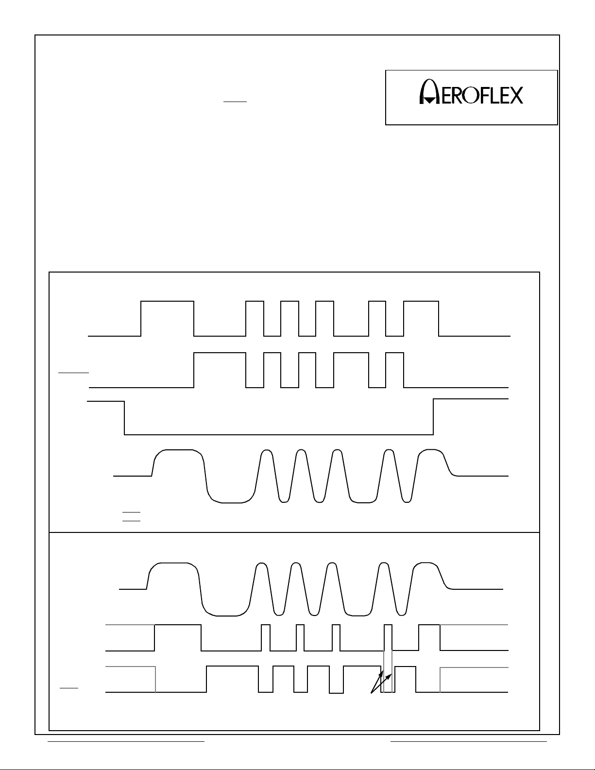
Transmitter
The Transmitter section accepts
bi-phase TTL data at the input and
when coupled to the data bus with a
primary grounded center tap
1:2.5
transformer, isolated on the
data bus side with two 52.5 Ohm fault
isolation resistors, and loaded by two
70 Ohm terminations plus additional
receivers, the data bus signal
produced is 7.5Volts nominal P-P at
A-A’ (See Figure 5). When both DATA
and DATA
the transmitter output becomes a
inputs are held low or high,
TX DATA IN
TX DATA IN
TX INHIBIT
+5 V
GROUND
STROBE
DRIVER
INPUT
AMP
SHAPING
REFERENCE
ACTIVE
FILTER
OUTPUT
STAGE
COMP.
COMP.
TX/RX
TX/RX
RX DATA OUT
RX DATA OUT
high impedance and is “removed”
Block Diagram
from the line. In addition, an
eroflex Circuit Technology – Data Bus Modules For The Future © SCD4419 REV B 10/21/99
Page 2
Aeroflex Circuit Technology
SCD4419 REV B 10/21/99 Plainview NY (516) 694-6700
CIRCUIT TECHNOLOGY
level devices, the receiver outputs are swapped as shown by the dashed lines.
overriding “INHIBIT" input provides
for the removal of the transmitter
output from the line. A logic “1”
applied to the “INHIBIT” takes priority
over the condition of the data inputs
and disables the transmitter. (See
Transmitter Logic Waveform, Figure
1).
The transceiver utilizes an active
filter to suppress harmonics above
1MHz. The Transmitter may be
safely operated at 100% duty cycle
for an indefinite period into a short
circuited 1553 bus.
Figure 1 - Transmitter Logic Waveforms
DATA IN
Receiver
The Receiver section accepts
bi-phase differential data at the input
and produces two TTL signals at the
output. The outputs are DATA and
, and represent positive and
DATA
negative excursions of the input
beyond a pre-determined threshold.
(See Receiver Logic Waveform.
Figure 2).
The pre-set internal thresholds will
detect data bus signals exceeding
1.150 Volts P-P and reject signals
less than 0.6 volts P-P when used
with a 1:2.5 turns ratio transformer.
(See Figure 5 for transformer data
and typical connection).
DATA IN
INHIBIT
LINE TO LINE
OUTPUT
NOTES:
1.DATA and DATA
2.DATA and DATA
inputs must be complementary waveforms or 50% duty cycle average, with no delays between them.
must be in the same state during off time (both high or low).
Figure 2 - Receiver Logic Waveforms
LINE TO LINE
INPUT
DATA OUT
OUT
DATA
NOTE: Waveforms shown are for normally low devices. For normally high receiver output
Note overlap
2
Page 3

Aeroflex Circuit Technology
SCD4419 REV B 10/21/99 Plainview NY (516) 694-6700
Absolute Maximum Ratings
Operating Case Temperature -55°C to +125°C
Storage Case Temperature -65°C to +150°C
Positive Power Supply Voltage +5.0 V to +7.0 V
Receiver Differential Input ±10 V
Receiver Input Voltage (Common Mode) ±5 V
Driver Peak Output Current 650 mA
Total Package Power Dissipation over the Full Operating Case
2 Watt
Temperature Rise
Maximum Junction To Case Temperature Rise for the Hottest
Device
10°C
Thermal Resistance, Junction to Bottom of Case 5°C/W
Electrical Characteristics – Driver Section
Input Characteristics, TX DATA in or TX DATA in
Parameter Condition Symbol Min Typ Max Unit
"0" Input Current VIN = 0.4 V I
"1" Input Current V
= 2.7 V I
IN
"0" Input Voltage V
"1" Input Voltage V
Inhibit Characteristics
"0" Input Current
"1" Input Current V
"0" Input Voltage
"1" Input Voltage
Delay from TX inhibit,(0→1) to inhibited output
Delay from TX inhibit, (1→0) to active output
Differential Output Noise, inhibit mode
Differential Output Impedance (inhibited)
V
=0.4V
IN
IN
Note 1
=2.7V
Output Characteristics
Differential output level
Rise And Fall Times(10% to 90% of p-p output)
Output Offset at point A-A’on Fig 5., 2.5 µS
after midpoint crossing of the parity bit of the
last word of a 660 µS message
Delay from 50% point of TX DATA or TX
input to zero crossing of differential
DATA
signal
Control Voltage Slope
0 – 5 Vdc measured at Pt A - A’
0 – 10 Vdc measured at Pt A - A’
Pt. A - A’
=35 Ω
R
L
L = 1 mA
I
max
ILD
IHD
IHD
IHD
I
ILI
I
IHI
V
ILI
V
IHI
t
DXOFF
t
DXON
V
NOI
Z
OI
V
t
V
OS
t
DTX
-0.2 -0.4
mA
1 40 µA
0.7
V
2.0 V
-0.2 -0.4
1.0 40
0.7
2
200 300
80 150
mA
µA
V
V
nS
nS
2 10 mVp-p
2K
O
r
6 7.5 8 V p-p
100 170 300 nS
±90
100 150
1.1
0.55
1.5
0.75
1.9
0.95
Ω
mV peak
nS
Vp-p/Vdc
Vp-p/Vdc
3
Page 4

Aeroflex Circuit Technology
SCD4419 REV B 10/21/99 Plainview NY (516) 694-6700
Electrical Characteristics – Receiver Section
Parameter Condition Symbol Min Typ Max Unit
Differential Voltage Range, Figure 4 Point P-P’ V
IDR
Common Mode Rejection Ratio CMRR
45 dB
20
Strobe Characteristics (Logic "0" inhibits output) if not used, a 1K pullup to 5 V is recommended
"0" Input Current VS=0.4 V
"1" Input Current
=2.7V I
V
S
"0" Input Voltage
"1" Input Voltage V
Strobe Delay (turn-on)
Strobe Delay (turn-off)
I
IL
IH
V
IL
IH
t
SD(ON)
t
SD(OFF)
2.0
-0.2
1 +40
40 100
60 100
-0.4
0.7
Threshold Characteristics (Sinewave input )
Input Threshold Voltage(referred to the bus)
100KHz-
1MHz
V
TH
0.60 0.8 1.15
Output Characteristics, RX DATA and RX DATA
"1" State IOH=-0.4 mA
V
OH
2.5 3.7 V
V peak
mA
µA
V
V
nS
nS
V
p-p
"0" State I
Delay, (average)from differential input zero
crossings to RX DATA and RX DATA
output
= 4 mA
OL
V
t
DRX
OL
0.3
0.5
250 400 nS
V
50% points
Power Data
Maximum Currents, Per Channel (+5V)
Duty Cycle Typ Max
Transmitter Standby
25% duty cycle
50% duty cycle
100% duty cycle
Power Supply Voltage
+V 4.75 to 5.5 Volts
Notes: 1. Power ON/OFF, measured from 75KHz to 1MHz at Point A-A. See Figure 5
2. V
3. Specifications apply over the case temperature range of -55°C to +125°C unless otherwise specfied.
4. All typical values are measured at +25°C
= 5 volts ±0.1 V, for all measurements unless otherwise specified.
cc
20 mA 30 mA
155 mA 185 mA
290 mA 335 mA
560 mA 650 mA
4
Page 5

Aeroflex Circuit Technology
SCD4419 REV B 10/21/99 Plainview NY (516) 694-6700
POWER DISSIPATION
MILLIWATTS
Figure 3 – Transmitter (TX) Output Amplitude
OUTPUT AMPLITUDE
vs Control Voltage
VP-P @ B–B'
7.5
6.75
5.25
4.5
3.75
2.25
1.5
.75
Slope = 0.75 VP-P/Vdc for 10V
Slope = 1.5 V
6
3
0
0 1 2 3 4 5 6 7 8 9 10
P-P/Vdc for 5V
Typical
CONTROL VOLTAGE
Vdc
7.5
4.5
1.5
Figure 4 – Transmitter (TX) Output Offset
LAST BIT
Magnified View
0 volts
6
2.5 µsec
3
*Offset measured at point A-A’ in Fig 5
OUTPUT OFFSET*
OUTPUT OFFSET
*
Figure 5 – Typical Transformer Connection
70
Ω 70Ω
ZO
TX DATA OUT
D.U.T
TX DATA
OUT
RX DATA
RX DATA IN
IN
1:2.5
P
P’
55Ω
B
B’
Center
55Ω
Tap
A
A’
1:1.77 for
stub
coupling
Figure 6 – Power Dissipation vs. Duty Cycle
1600
1400
1200
1000
800
600
400
200
0
0 10 20 30 40 50 60 70 80 90 100
Maximum
Typical
DUTY CYCLE – PERCENT
Transformer
Use Technitrol 1553-45 or Equivalent
Note: Vcc = 5 Volts, V
(pt A-A') at 7.5 Volts P-P
bus
5
Page 6

Aeroflex Circuit Technology
SCD4419 REV B 10/21/99 Plainview NY (516) 694-6700
Plainview New York 11803
Toll Free Inquiries: 1-(800)THE-1553
CIRCUIT TECHNOLOGY
PLUG-IN PACKAGE
1.27 MAX
1.10
24
1.27
MAX
1
0.24
MIN
0.018 DIA.
±0.002
Notes
1. Dimensions shown are in inches
2. Pins are equally spaced at 0.10.0±0.002 tolerance, non-cumulative, each row.
13
1.10
12
0.175
0.100
Pin Connections
1. TX DATA OUT
2. TX DATA OUT
3. TX GND (+5)
4. N.C.
5. N.C.
6. N.C.
7. RX DATA OUT
8. STROBE
9. RX GND (+5V)
10.RXDATA
11. N.C.
12. N.C.
13. N.C.
14. N.C.
15. RX DATA IN
16. RX DATA
17. GND
18. CASE GND
19. N.C.
MAX
20. +5V
21. TX INHIBIT
22. TX DATA IN
23. TX DATA
24. N.C.
OUT
1.27 MAX
IN
IN
FLAT PACKAGE
1.27 MAX
1
Dot indicates Pin 1
0.167 for Low Profile Flat Pack
0.200 for Std Flat Pack
0.400
MAX
0.080
±0.015
±0.002
2 sides
0.009
±0.002
0.017
0.10 Typ
Configurations and Ordering Information
Model No. DESC No. Receiver Data level Case Specs. Configuration
ACT4419 Pending Normally Low Plug In 1553 & 1760 Single
ACT4419FP Pending Normally Low Flat Pack 1553 & 1760 Single
Specifications subject to change without notice.
Aeroflex Circuit Technology
35 South Service Road
Telephone: (516) 694-6700
FAX: (516) 694-6715
6
 Loading...