

Page 1

Description
ACSL-6xx0 are truly isolated,
multi-channel and bi-directional,
high-speed optocouplers. Integration of multiple optocouplers in
monolithic form is achieved
through patented process technology. These devices provide full
duplex and bi-directional isolated data transfer and communication capability in compact
surface mount packages. Available in 15 Mbd speed option and
wide supply voltage range.
These high channel density make
them ideally suited to isolating
data conversion devices, parallel
buses and peripheral interfaces.
Agilent ACSL-6xx0
Multi-Channel and Bi-Directional,
15 MBd Digital Logic Gate Optocoupler
Data Sheet
Features
• Available in dual, triple and quad
channel configurations
• Bi-directional
Applications
• Full duplex communication
• Isolated line receiver
• Computer-peripheral interfaces
• Microprocessor system interfaces
• Digital isolation for A/D and D/A
conversion
• Switching power supply
• Instrument input/output isolation
• Ground loop elimination
• Pulse transformer replacement
• Wide supply voltage range
3.0V to 5.5V
• High-speed: 15 MBd typical,
10 MBd minimum
• 10 kV/µs minimum Common Mode
Rejection (CMR) at Vcm = 1000V
• LSTTL/TTL compatible
• Safety and regulatory approvals
(Pending)
– 2500Vrms for 1 min per UL1577
– CSA Component Acceptance
– IEC/EN/DIN EN 60747-5-2
• 16 Pin narrow-body SOIC package
for triple and quad channel
• -40 to 100°C temperature range
They are available in 8-pin and
16–pin narrow-body SOIC
package and are specified over
the temperature range of
-40°C to +100° C.
CAUTION:
It is advised that normal static precautions be taken in handling and
assembly of this component to prevent damage and/or degradation,
which may be induced by ESD.
Page 2

Device Selection Guide
Device Number Channel Configuration Package
ACSL-6210 Dual, Bi-Directional` 8-pin Small Outline
ACSL-6300* Triple, All-in-One 16-pin Small Outline
ACSL-6310* Triple, Bi-Directional, 2/1 16-pin Small Outline
ACSL-6400 Quad, All-in-One 16-pin Small Outline
ACSL-6410* Quad, Bi-Directional, 3/1 16-pin Small Outline
ACSL-6420* Quad, Bi-Directional, 2/2 16-pin Small Outline
* Advanced Information
Ordering Information
A C S L - 6 X X 0 - X Y Z E
Lead Free Option
Channel Configuration
(Refer to the Device
Selection Guide)
R = SO-8 Package, 100 units per tube
T = SO-16 Package, 50 units per tube
6 = IEC/EN/DIN EN 60747-5-2,
VIORM = 560V peak Option
5 = Tape and Reel Packaging Option,
1500 units per reel for SO-8 Package
and 1000 units per reel for SO-16 Package
Pin Description
Symbol Description Symbol Description
V
DD1
V
DD2
ANODE
CATHODE
x
Power Supply 1 GND
Power Supply 2 GND
LED Anode NC Not Connected
LED Cathode V
x
1
2
OX
Power Supply Ground 1
Power Supply Ground 2
Output Signal
Truth Table (Positive Logic)
LED OUTPUT
ON L
OFF H
2
Page 3
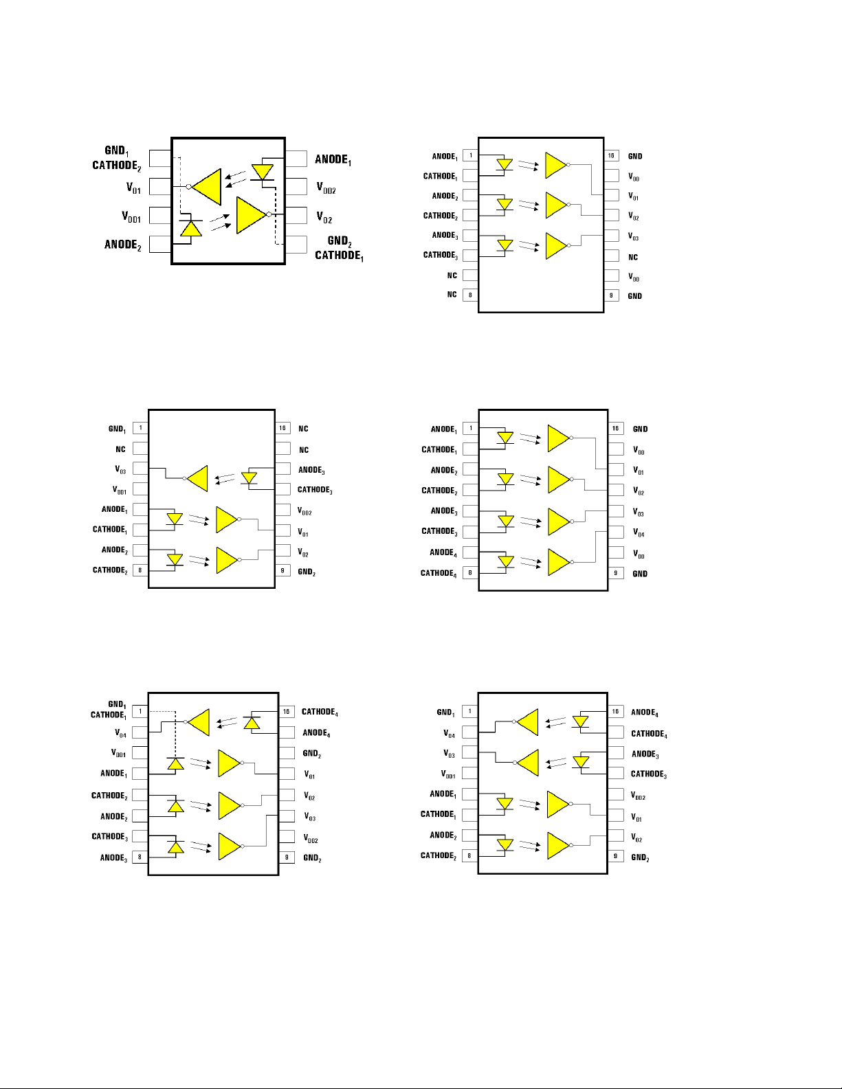
Functional Diagrams
ACSL-6210 - Dual-Ch, Bi-Dir ACSL-6300 - Triple-Ch, All-in-One*
ACSL-6310 - Triple-Ch, Bi-Dir (2/1)* ACSL-6400 - Quad-Ch, All-in-One
ACSL-6410 - Quad-Ch, Bi-Dir (3/1)* ACSL-6420 - Quad-Ch, Bi-Dir (2/2)*
* Advanced Information
3
Page 4

P
Package Outline Drawings
ACSL-6210 Small Outline SO-8 Package
0.189 (4.80)
0.197 (5.00)
0.228 (5.80)
0.244 (6.20)
87
1
0.013 (0.33)
0.020 (0.51)
2
65
4
3
0.150 (3.80)
0.157 (4.00)
0.010 (0.25)
0.020 (0.50)
x 45°
0.054 (1.37)
0.069 (1.75)
0.040 (1.016)
0.060 (1.524)
DIMENSIONS: INCHES (MILLIMETERS)
0.004 (0.10)
0.010 (0.25)
MIN
MAX
ACSL-6300*, ACSL-6310*, ACSL-6400, ACSL-6410* and
ACSL-6420* Small Outline SO-16 Package
0.386 (9.
802
)
0.394 (9.
999
)
18
0.016 (0.40)
0.050 (1.27)
0.008 (0.19)
0.010 (0.25)
0°
8°
0.228 (5.
791
)
0.244 (6.
197
)
0.013 (0.
0.020 (0.
0.050 (1.
270
)
0.060 (1.
524
)
0.040 (1.
016
)
0.060 (1.
524
)
DIMENSIONS: INCHES (MILLIMETERS)
4
330
508
MIN
MAX
0.152 (3.
861
)
0.157 (3.
988
)
)
)
0.004 (0.
0.010 (0.
0.054 (1.
0.068 (1.
102
)
249
)
372
727
)
0.008 (0.
191
0.010 (0.
249
)
)
)
0.010 (0.
245
)
x
508
0° –
0.016 (0.
0.050 (1.
)
45°ß
8° TY
406
270
)
)
0.020 (0.
Page 5

Solder Reflow Temperature Profile
300
PREHEATING RATE 3°C + 1°C/–0.5°C/SEC.
REFLOW HEATING RATE 2.5°C ± 0.5°C/SEC.
200
160°C
150°C
140°C
3°C + 1°C/–0.5°C
100
TEMPERATURE (°C)
ROOM
TEMPERATURE
0
0
50 150100 200 250
2.5°C ± 0.5°C/SEC.
PREHEATING TIME
150°C, 90 ± 30 SEC.
PEAK
TEMP.
245°C
TIME (SECONDS)
SEC.
30
SEC.
30
SOLDERING
TIME
200°C
50 SEC.
PEAK
TEMP.
240°C
PEAK
TEMP.
230°C
TIGHT
TYPICAL
LOOSE
Pb-free IR Profile
5
Page 6

Regulatory Information
Insulation and Safety Related Specifications
Parameter Symbol Value Units Conditions
Minimum External Air Gap (Clearance) L(I01) 4.9 mm Measured from input terminals to output terminals,
shortest distance through air
Minimum Externa l Tracking(Creepage) L(I02) 4.5 mm Measured from input terminals to output terminals,
shortest distance path through body
Minimum Internal Plastic Gap (Internal Clearance) 0.08 mm Insulation thickness between emitter and detector;
also known as distance through insulation
Tracking Resistance (Comparative Tracking Index) CTI 175 Volts DIN IEC 112/VDE0303 Part 1
Isolation Group IIIa Material Group (DIN VDE 0110, 1/89, Table 1)
IEC/EN/DIN EN 60747-5-2 Insulation Related Characteristics (Option X6X Only)
Description Symbol ACSL-6XX0-X6X Units
Installation Classification per DIN VDE 0110/1.89, Table 1
for rated mains voltage ≤ 150V rms I-IV
for rated mains voltage ≤ 300V rms I-III
Climatic Classification 55/100/21
Pollution Degree (DIN VDE 0110/1.89) 2
Maximum Working Insulation Voltage V
Input to Output Test Voltage, Method b * V
V
x 1.875 = VPR, 100% Production
IORM
Test with tm = 1 sec, Partial Discharge < 5 pC
Input to Output Test Voltage, Method a * V
V
IORM
x 1.5 = V
Type and Sample Test,
PR,
IORM
PR
PR
Tm = 60 sec, Partial Discharge < 5 pC
Highest Allowable Overvoltage * V
(Transient Overvoltage, t
= 10 sec)
ini
IOTM
Safety Limiting Values
(Maximum values allowed in the event of a failure)
Case Temperature T
Input Current I
Output Power P
Insulation Resistance at TS, VIO = 500V R
S
S,INPUT
S,OUTPUT
IO
*Refer to the front of the optocoupler section of the current catalog, under Product Safety Regulations section, IEC/EN/DIN EN 60747-5-2,
for a detailed description.
Note: Isolation characteristics are guaranteed only within the safety maximum ratings, which must be ensured by protective circuits in application.
560 V
1050 V
840 V
4000 V
peak
peak
peak
peak
175 °C
150 mA
600 mW
9
10
Ω
6
Page 7

Absolute Maximum Ratings
Parameter Symbol Min. Max. Units
Storage Temperature T
Operating Temperature T
Supply Voltage (1 Minute Maximum) V
Reverse Input Voltage (Per Channel) V
Output Voltage (Per Channel) V
Average Forward Input Current
[1]
(Per Channel) I
Output Current (Per Channel) I
Input Power Dissipation
Output Power Dissipation
[2]
(Per Channel) P
[2]
(Per Channel) P
s
A
, V
DD1
DD2
R
O
F
O
1
O
-55 125 °C
-40 100 °C
7V
5V
7V
15 mA
50 mA
27 mW
60 mW
Recommended Operating Conditions
Parameter Symbol Min. Max. Units
Operating Temperature T
Input Current, Low Level
Input Current, High Level
[3]
[4]
Supply Voltage V
A
I
FL
I
FH
, V
DD1
DD2
Fan Out (at TA= 1kΩ) N 5 TTL Loads
Output Pull-up Resistor R
L
-40 100 °C
0 250 µA
715mA
3.0 5.5 V
330 4k Ω
Notes:
1. Peaking circuits may produce transient input
currents up to 50 mA, 50 ns max. pulse width,
provided average current does not exceed its
max. values.
2. Derate total package power dissipation, P
T
linearly above +80°C free-air temperature at a
rate of 5.45 mW/°C for the SO8 package.
PT=number of channels multiply by (PI+PO).
For SO16 package data, contact factory for
assistance.
3. The off condition can be guaranteed by
ensuring that VFL ≤ 0.8V.
4. The initial switching threshold is 7 mA or
less. It is recommended that minimum 8 mA
be used for best performance and to permit
guardband for LED degradation.
7
Page 8

Electrical Specifications
Over recommended operating range (3.0V ≤ V
unless otherwise specified.
All typical specifications are at T
= +25°C , V
A
≤ 3.6V, 3.0V ≤ V
DD1
= V
DD2
= +3.3V.
DD1
≤ 3.6V, TA = -40°C to +100° C)
DD2
Parameter Symbol Min. Typ. Max. Units Test Conditions
Input Threshold Current I
High Level Output Current I
Low Level Output Voltage V
High Level Supply Current (per channel) I
Low Level Supply Current (per channel) I
Input Forward Voltage V
Input Reverse Breakdown Voltage BV
TH
OH
OL
DDH
DDL
F
R
Input Diode Temperature Coefficient ∆VF / ∆T
Input Capacitance C
IN
1.25 1.52 1.80 V IF= 10 mA, TA=25°C
5.0 V IR=10 µA
A
2.7 7.0 mA I
4.7 100.0 µAI
0.36 0.68 V I
=13 mA, VO= 0.6V
OL(Sinking)
= 250 µA, VO= 3.3V
F
= 13 mA, IF= 7mA
OL(Sinking)
3.2 5.0 mA IF=0 mA
4.6 7.5 mA IF= 10 mA
-1.8 mV/°CI
=10 mA
F
80 pF f = 1 MHz, VF= 0V
Switching Specifications
Over recommended operating range (3.0V ≤ V
unless otherwise specified.
All typical specifications are at T
= +25°C , V
A
≤ 3.6V, 3.0V ≤ V
DD1
= V
DD2
= +3.3V.
DD1
≤ 3.6V, IF = 8.0 mA, TA = -40°C to +100°C)
DD2
Parameter Symbol Min. Typ. Max. Units Test Conditions
Maximum Data Rate 10 15 MBd RL = 350Ω, CL = 15 pF
Pulse Width t
Propagation Delay Time to Logic High Output Level
Propagation Delay Time to Logic Low Output Level
Pulse Width Distortion |t
Propagation Delay Skew
– t
| |PWD| 8 35 ns RL = 350Ω, CL = 15 pF
PHL
PLH
[7]
[5]
[6]
Output Rise Time (10 – 90%) t
Output Fall Time (10 – 90%) t
Logic High Common Mode Transient Immunity
Logic Low Common Mode Transient Immunity
[8]
[8]
PW
t
PLH
t
PHL
t
PSK
R
F
|CMH| 10 kV/µsV
|CML| 10 kV/µsV
100 ns RL = 350Ω, CL = 15 pF
52 100 ns RL = 350Ω, CL = 15 pF
44 100 ns RL = 350Ω, CL = 15 pF
40 ns RL = 350Ω, CL = 15 pF
35 ns RL = 350Ω, CL = 15 pF
12 ns RL = 350Ω, CL = 15 pF
= 1000V, IF = 0 mA,
cm
VO = 2.0V, RL = 350Ω,
TA = 25°C
= 1000V, IF = 8 mA,
cm
VO = 0.8V, RL = 350Ω,
TA = 25°C
Notes:
5. t
is measured from the 4.0 mA level on the
PLH
falling edge of the input pulse to the 1.5V
level on the rising edge of the output pulse.
6. t
is measured from the 4.0 mA level on the
PHL
rising edge of the input pulse to the 1.5V level
on the falling edge of the output pulse.
7. t
is equal to the worst case difference in
PSK
t
and/or t
PHL
units at any given temperature and specified
that will be seen between
PLH
test conditions.
8
8. CMH is the maximum common mode voltage
slew rate that can be sustained while
maintaining VO > 2.0V. CML is the maximum
common mode voltage slew rate that can be
sustained while maintaining VO < 0.8V. The
common mode voltage slew rates apply to
both rising and falling common mode voltage
edges.
Page 9

Electrical Specifications
Over recommended operating range (4.5V ≤ V
unless otherwise specified.
All typical specifications are at T
= +25°C, V
A
≤ 5.5V, 4.5V ≤ V
DD1
= V
DD2
= +5.0V.
DD1
≤ 5.5V, TA = -40°C to +100° C)
DD2
Parameter Symbol Min. Typ. Max. Units Test Conditions
Input Threshold Current I
High Level Output Current I
Low Level Output Voltage V
High Level Supply Current (per channel) I
Low Level Supply Current (per channel) I
Input Forward Voltage V
Input Reverse Breakdown Voltage BV
TH
OH
OL
DDH
DDL
F
R
Input Diode Temperature Coefficient ∆VF / ∆T
Input Capacitance C
IN
1.25 1.52 1.8 V IF = 10 mA, TA = 25°C
5.0 V IR = 10 µA
A
2.7 7.0 mA I
3.8 100.0 µAI
0.36 0.6 V I
=13 mA, VO= 0.6V
OL(Sinking)
= 250 µA, VO= 5.5V
F
=13 mA, IF=7 mA
OL(Sinking)
4.3 7.5 mA IF = 0 mA
5.8 10.5 mA IF = 10 mA
-1.8 mV/°CIF = 10 mA
80 pF f = 1 MHz, VF = 0V
Switching Specifications
Over recommended operating range (4.5V ≤ V
unless otherwise specified.
All typical specifications are at T
=+25° C, V
A
≤ 5.5V, 4.5V ≤ V
DD1
= V
DD1
DD2
= +5.0V.
≤ 5.5V, IF = 8.0 mA, TA = -40°C to +100°C)
DD2
Parameter Symbol Min. Typ. Max. Units Test Conditions
Maximum Data Rate 10 15 MBd RL = 350Ω, CL =15 pF
Pulse Width t
Propagation Delay Time to Logic High Output Level
Propagation Delay Time to Logic Low Output Level
Pulse Width Distortion |t
Propagation Delay Skew
– t
| |PWD| 5 35 ns RL = 350Ω, CL =15 pF
PHL
PLH
[7]
[5]
[6]
Output Rise Time (10 – 90%) t
Output Fall Time (10 – 90%) t
Logic High Common Mode Transient Immunity
Logic Low Common Mode Transient Immunity
[8]
[8]
PW
t
PLH
t
PHL
t
PSK
R
F
|CMH| 10 kV/µsVcm= 1000V, IF=0 mA,
|CML| 10 kV/µsVcm= 1000V, IF= 8 mA,
100 ns RL = 350Ω, CL =15 pF
46 100 ns RL = 350Ω, CL =15 pF
43 100 ns RL = 350Ω, CL =15 pF
40 ns RL = 350Ω, CL =15 pF
30 ns RL = 350Ω, CL =15 pF
12 ns RL = 350Ω, CL =15 pF
VO = 2.0V, RL=350Ω,
TA = 25°C
VO = 0.8V, RL= 350Ω,
TA = 25°C
Notes:
5. t
is measured from the 4.0 mA level on the
PLH
falling edge of the input pulse to the 1.5V
level on the rising edge of the output pulse.
6. t
is measured from the 4.0 mA level on the
PHL
rising edge of the input pulse to the 1.5V level
on the falling edge of the output pulse.
7. t
is equal to the worst case difference in
PSK
t
PHL
and/or t
that will be seen between
PLH
units at any given temperature and specified
test conditions.
9
8. CMH is the maximum common mode voltage
slew rate that can be sustained while
maintaining VO > 2.0V. CML is the maximum
common mode voltage slew rate that can be
sustained while maintaining VO < 0.8V. The
common mode voltage slew rates apply to
both rising and falling common mode voltage
edges.
Page 10

Package Characteristics
All specifications are at TA=+25°C.
Parameter Symbol Min. Typ. Max. Units Test Conditions
Input-Output Momentary SO8 V
Withstand Voltage
Input-Output Insulation
[9]
[10] [11]
SO16 V
SO8 I
SO16 I
Input-Output Resistance
[10]
SO8 R
SO16 R
Input-Output Capacitance
[10]
SO8 C
SO16 C
Input-Input Insulation SO8 I
Leakage Current
Input-Input Resistance
[12]
[12]
SO16 I
SO8 R
SO16 R
Input-Input Capacitance
[12]
SO8 C
SO16 C
Electrostatic Discharge Sensitivity
This product has been tested for
Notes:
9. V
electrostatic sensitivity to the
limits stated in the specifications.
However, Agilent recommends
that all integrated circuits be
handled with appropriate care to
avoid damage. Damage caused by
inappropriate handling or storage
could range from performance
10. Measured between each input pair shorted
degradation to complete failure.
ISO
ISO
I-O
I-O
I-O
I-O
I-O
I-O
I-I
I-I
I-I
I-I
I-I
I-I
is a dielectric voltage rating that should
ISO
not be interpreted as an input-output
2500 V
2500 RH ≤ 50%, t = 1 min
9
10
9
10
11
10
11
10
0.7 pF f = 1 MHz
0.7 f = 1 MHz
0.005 µARH≤45%, t = 5 sec, V
0.005 RH ≤45%, t =5 sec, V
11
10
11
10
0.1 pF f = 1 MHz
0.12 f = 1 MHz
continuous voltage rating. For continuous
voltage rating, refer to the IEC/EN/DIN EN
60747-5-2 Insulation Characteristics Table (if
applicable), the equipment level safety
specification or Agilent Application Note
1074 entitled “Optocoupler Input-Output
Endurance Voltage.”
together and all output connections for that
channel shorted together.
RMS
RH ≤50%, t = 1 min
5 µA 45% RH, t =5 sec, V
5 45% RH, t= 5 sec, V
Ω V
= 500V DC
I-O
V
= 500V DC
I-O
Ω RH≤ 45%, t =5 sec, V
RH ≤45%, t =5 sec, V
11. In accordance to UL1577, each optocoupler
is proof tested by applying an insulation test
voltage ≥ 3000 Vrms for 1 sec (leakage
detection current limit, I
≤ 5 µA). This test
I-O
is performed before the 100% production test
for partial discharge (Method b) shown in the
IEC/EN/DIN EN 60747-5-2 Insulation
Characteristics Table, if applicable.
12. Measured between inputs with the LED
anode and cathode shorted together.
= 3kV DC
I-O
=3kV DC
I-O
= 500V
I-I
= 500V
I-I
= 500V
I-I
=500V
I-I
www.agilent.com/semiconductors
For product information and a complete list of
distributors, please go to our web site.
For technical assistance call:
Americas/Canada: +1 (800) 235-0312 or
(916) 788-6763
Europe: +49 (0) 6441 92460
China: 10800 650 0017
Hong Kong: (65) 6756 2394
India, Australia, New Zealand: (65) 6755 1939
Japan: (+81 3) 3335-8152(Domestic/International), or
0120-61-1280(Domestic Only)
Korea: (65) 6755 1989
Singapore, Malaysia, Vietnam, Thailand, Philippines,
Indonesia: (65) 6755 2044
Taiwan: (65) 6755 1843
Data subject to change.
Copyright © 2004 Agilent Technologies, Inc.
November 1, 2004
5989-1343EN
 Loading...