

Page 1
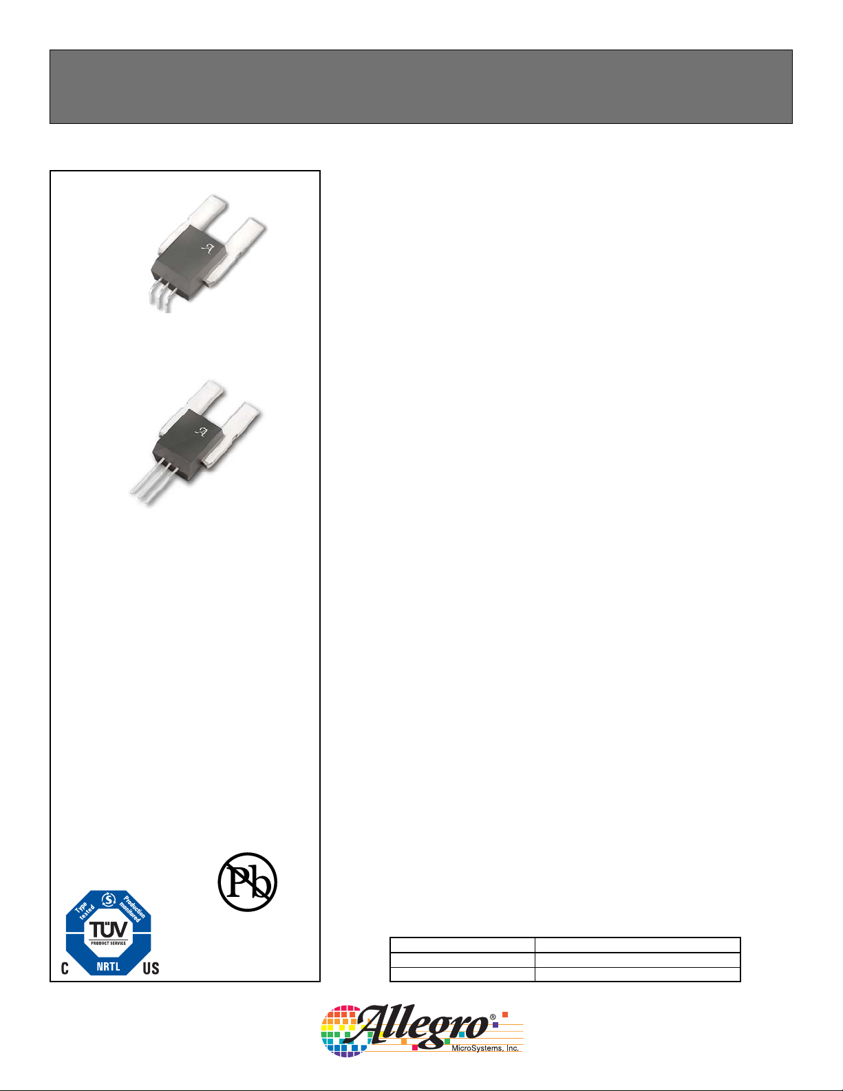
Current Sensor: ACS754SCB-200
5
4
1
2
3
Package CB-PSF
5
4
1
2
3
Package CB-PSS
Pin 1: VCC
Pin 2: GND
Pin 3: VOUT
AB SO LUTE MAX I MUM RAT INGS
Supply Voltage, VCC..........................................16 V
Reverse Supply Voltage, V
Output Voltage, V
Reverse Output Voltage, V
Output Current Source, I
Output Current Sink, I
Operating Temperature,
Ambient, T
Maximum Junction, T
Maximum Storage Temperature, T
OUT
, S range ....................... –20 to 85ºC
A
Terminal 4: IP+
Terminal 5: IP–
........................–16 V
RCC
........................................16 V
...................... –0.1 V
ROUT
OUT(Source)
OUT(Sink)
.......................10 mA
....................... 165°C
J(max)
S
................. 3 mA
....–65 to 170°C
The Allegro ACS75x family of current sensors provides economical and
precise solutions for current sensing in industrial, automotive, commercial, and
communications systems. The device package allows for easy implementation
by the customer. Typical applications include motor control, load detection and
management, power supplies, and overcurrent fault protection.
The device consists of a precision, low-offset linear Hall sensor circuit with a
copper conduction path located near the die. Applied current fl owing through
this copper conduction path generates a magnetic fi eld which is sensed by the
integrated Hall IC and converted into a proportional voltage. Device accuracy
is optimized through the close proximity of the magnetic signal to the Hall
transducer. A precise, proportional voltage is provided by the low-offset, chopperstabilized BiCMOS Hall IC, which is programmed for accuracy at the factory.
The output of the device has a positive slope (>V
/ 2) when an increasing
CC
current fl ows through the primary copper conduction path (from terminal 4 to
terminal 5), which is the path used for current sensing. The internal resistance of
this conductive path is typically 100 µΩ, providing low power loss. The thickness
of the copper conductor allows survival of the device at up to 5× overcurrent
conditions. The terminals of the conductive path are electrically isolated from the
sensor leads (pins 1 through 3). This allows the ACS75x family of sensors to be
used in applications requiring electrical isolation without the use of opto-isolators
or other costly isolation techniques.
The device is fully calibrated prior to shipment from the factory. The ACS75x
family is lead-free. All leads are coated with 100% matte tin, and there is no lead
inside the package. The heavy gauge leadframe is made of oxygen-free copper.
Features and Benefi ts
• Monolithic Hall IC for high reliability
• Single +5 V supply
• 3 kV
isolation voltage between terminals 4/5 and pins 1/2/3
RMS
• 35 kHz bandwidth
• End-of-line factory-trimmed for gain and offset
• Ultra-low power loss: 100 µΩ internal conductor resistance
• Ratiometric output from supply voltage
• Extremely stable output offset voltage
• Small package size, with easy mounting capability
• Output proportional to ac and dc currents
Applications
• Industrial systems
• Motor control
• Servo systems
• Power conversion
• Battery monitors
TÜV America
Certifi cate Number:
U8V 04 11 54214 001
ACS754200-DS, Rev. 3
Use the following complete part numbers when ordering:
Part Number Package
ACS754SCB-200-PSF Formed signal pins
ACS754SCB-200-PSS Straight signal pins
115 Northeast Cutoff, Box 15036
Worcester, Massachusetts 01615-0036 (508) 853-5000
Page 2
Current Sensor: ACS754SCB-200
Functional Block Diagram
+5 V
IP–
Terminal 5
Cancellation
Dynamic Offset
Gain
VCC
Pin 1
Voltage
Regulator
To all subcircuits
Amp Out
Temperature
Coefficient
Filter
Trim Control
Offset
VOUT
Pin 3
0.1 µF
ACS754200-DS, Rev. 3
IP+
Terminal 4
GND
Pin 2
115 Northeast Cutoff, Box 15036
Worcester, Massachusetts 01615-0036 (508) 853-5000
2
Page 3

Current Sensor: ACS754SCB-200
ELECTRICAL CHARACTERISTICS, over operating ambient temperature range unless otherwise stated
Characteristic Symbol Test Conditions Min. Typ. Max. Units
Primary Sensed Current I
Supply Voltage V
Supply Current I
Output Resistance R
Output Capacitance Load C
Output Resistive Load R
Primary Conductor Resistance R
Isolation Voltage V
P
CC
CC
OUT
LOAD
LOAD
PRIMARYIP
ISO
VCC = 5.0 V, output open 6.5 8 10 mA
I
= 1.2 mA – 1 2 Ω
OUT
VOUT to GND – – 10 nF
VOUT to GND 4.7 – – kΩ
= ±50A; TA = 25°C – 100 – µΩ
Pins 1-3 and 4-5; 60 Hz, 1 minute 3.0 – – kV
PERFORMANCE CHARACTERISTICS, -20°C to +85°C, VCC = 5 V unless otherwise specifi ed
Propagation time t
Response time t
PROP
RESPONSEIP
Rise time t
r
IP = ±100 A, TA = 25°C – 4 – µs
= ±100 A, TA = 25°C – 11 – µs
IP = ±100 A, T A= 25°C – 10 – µs
Frequency Bandwidth f –3 dB, T = 25°C – 35 – kHz
Sensitivity Sens
Noise V
Nonlinearity E
Symmetry E
Zero Current Output Voltage V
Electrical Offset Voltage
(Magnetic error not included)
Magnetic Offset Error
Total Output Error
(Including all offsets)
NOISE
LIN
SYM
OUT(Q)
V
OE
I
ERROM
E
TOT
Over full range of IP , TA = 25°C – 10.0 – mV/A
Over full range of I
P
Peak-to-peak, TA = 25°C,
no external fi lter
Over full range of I
Over full range of I
P
P
I = 0 A, TA= 25°C – VCC / 2 – V
I = 0 A, TA = 25°C –10 – 10 mV
I = 0 A –20 – 20 mV
I = 0 A, after excursion of 200 A – ±0.15 ±0.50 A
Over full range of IP , TA = 25°C – ±1.0 – %
Over full range of I
P
–200 – 200 A
4.5 5.0 5.5 V
9.5 – 10.5 mV/A
–35 –mV
– – ±0.8 %
98 100 102 %
– – ±5.0 %
ACS754200-DS, Rev. 3
115 Northeast Cutoff, Box 15036
Worcester, Massachusetts 01615-0036 (508) 853-5000
3
Page 4

Current Sensor: ACS754SCB-200
Defi nitions of Accuracy Characteristics
Sensitivity (Sens): The change in sensor output in response to a 1 A change through the primary conductor. The sensitivity is the
product of the magnetic circuit sensitivity (G / A) and the linear IC amplifi er gain (mV/G). The linear IC amplifi er gain is trimmed at the
factory to optimize the sensitivity (mV/A) for the full-scale current of the device.
Noise (V
The noise fl oor is derived from the thermal and shot noise observed in Hall elements. Dividing the noise (mV) by the sensitivity (mV/
A) provides the smallest current that the device is able to resolve.
Linearity (E
its full-scale amplitude. Linearity reveals the maximum deviation from the ideal transfer curve for this transducer. Nonlinearity in the
output can be attributed to the gain variation across temperature and saturation of the fl ux concentrator approaching the full-scale cur-
rent. The following equation is used to derive the linearity:
where
∆ gain = the gain variation as a function of temperature changes from 25ºC,
% sat = the percentage of saturation of the fl ux concentrator, which becomes signifi cant as the current
being sensed approaches full-scale ±IP , and
V
Symmetry (E
tive full-scale primary current. The following equation is used to derive symmetry:
Quiescent output voltage (V
nominally remains at VCC ⁄ 2. Thus, VCC = 5 V translates into V
of the Allegro linear IC quiescent voltage trim, magnetic hysteresis, and thermal drift.
): The product of the linear IC amplifi er gain (mV/G) and the noise fl oor for the Allegro Hall effect linear IC (≈1 G).
NOISE
): The degree to which the voltage output from the sensor varies in direct proportion to the primary current through
LIN
OUT(Q)
)
[
)
[{
OUT(Q)
can be attributed to the resolution
out_full-scale amperes
): The degree to which the absolute voltage output from the sensor varies in proportion to either a positive or nega-
SYM
100
= the output voltage (V) when the sensed current approximates full-scale ±IP .
OUT(Q)
∆ gain × % sat (
1–
[{
2(V
V
100
[
V
): The output of the sensor when the primary current is zero. For a unipolar supply voltage, it
V
out_full-scale amperes
out_half-scale amperes
out_+full-scale amperes
–V
OUT(Q)
out_–full-scale amperes
OUT(Q)
= 2.5 V. Variation in V
– V
– V
OUT(Q)
– V
OUT(Q)
Electrical offset voltage (VOE): The deviation of the device output from its ideal quiescent value of VCC ⁄ 2 due to nonmagnetic causes.
Magnetic offset error (I
netic offset error is highest when the magnetic circuit has been saturated, usually when the device has been subjected to a full-scale or
high-current overload condition. The magnetic offset is largely dependent on the material used as a fl ux concentrator. The larger mag-
netic offsets are observed at the lower operating temperatures.
Accuracy (E
total ouput error. The accuracy is illustrated graphically in the Output Voltage versus Current chart on the following page.
Accuracy is divided into four areas:
• 0 A at 25°C: Accuracy of sensing zero current fl ow at 25°C, without the effects of temperature.
• 0 A over temperature: Accuracy of sensing zero current fl ow including temperature effects.
• Full-scale current at 25°C: Accuracy of sensing the full-scale current at 25°C, without the effects of temperature.
• Full-scale current over ∆ temperature: Accuracy of sensing full-scale current fl ow including temperature effects.
ACS754200-DS, Rev. 3
): The accuracy represents the maximum deviation of the actual output from its ideal value. This is also known as the
TOT
): The magnetic offset is due to the residual magnetism (remnant fi eld) of the core material. The mag-
ERROM
115 Northeast Cutoff, Box 15036
Worcester, Massachusetts 01615-0036 (508) 853-5000
4
Page 5

Current Sensor: ACS754SCB-200
Output voltage vs. current, illustrating sensor accuracy at 0 A and at full-scale current
–IP(A)
–200 A
Accuracy
vrOe∆Temperature
Accuracy
25°C Only
Increasing V
Average
V
OUT
(V)
OUT
Accuracy
25°C Only
Full Scale
200 A
Accuracy
vrOe∆Temperature
+IP(A)
ACS754200-DS, Rev. 3
Accuracy
25°C Only
Accuracy
vrOe∆Temperature
0A
Decreasing V
OUT
(V)
115 Northeast Cutoff, Box 15036
Worcester, Massachusetts 01615-0036 (508) 853-5000
5
Page 6

Current Sensor: ACS754SCB-200
Typical Percentage Error versus Ambient Temperature
5
4
3
2
1
0
(% of 200 A)
-1
TOT
-2
E
-3
-4
-5
-200 25557080
+ 3 Sigma
Mean
– 3 Sigma
TA (°C)
ACS754200-DS, Rev. 3
115 Northeast Cutoff, Box 15036
Worcester, Massachusetts 01615-0036 (508) 853-5000
6
Page 7

Current Sensor: ACS754SCB-200
Defi nitions of Dynamic Response Characteristics
Propagation delay (t
): The time required for the sensor output to refl ect a change in the primary current
PROP
signal. Propagation delay is attributed to inductive loading within the linear IC package, as well as in the inductive loop formed by the primary conductor geometry. Propagation delay can be considered as a fi xed time offset
and may be compensated.
Primary Current
Transducer Output
Propagation Time, t
PROP
t
Response time (t
RESPONSE
I (%)
90
0
): The time interval between a) when the primary current signal reaches 90% of its
fi nal value, and b) when the sensor reaches 90% of its output corresponding to the applied current.
I (%)
90
Primary Current
Transducer Output
Rise time (t
0
Response Time, t
): The time interval between a) when the sensor reaches 10% of its full scale value, and b) when
r
RESPONSE
t
it reaches 90% of its full scale value. The rise time to a step response is used to derive the bandwidth of the
current sensor, in which ƒ(–3 dB) = 0.35 / tr. Both tr and t
RESPONSE
are detrimentally affected by eddy current
losses observed in the conductive IC ground plane and, to varying degrees, in the ferrous fl ux concentrator
within the current sensor package.
Primary Current
Transducer Output
Rise Time, t
r
t
115 Northeast Cutoff, Box 15036
Worcester, Massachusetts 01615-0036 (508) 853-5000
ACS754200-DS, Rev. 3
I (%)
90
10
0
7
Page 8

Current Sensor: ACS754SCB-200
Standards and Physical Specifi cations
Parameter Specifi cation
Flammability (package molding compound) UL recognized to UL 94V-0
UL60950-1:2003
Fire and Electric Shock
Creepage distance, current terminals to sensor pins 7.25 mm
Clearance distance, current terminals to sensor pins 7.25 mm
Package mass 4.63 g typical
EN60950-1:2001
CAN/CSA C22.2 No. 60950-1:2003
Step Response, IP = 0 to 200 A, no external fi lter
ACS754 Output (mV)
Excitation Signal
ACS754200-DS, Rev. 3
115 Northeast Cutoff, Box 15036
Worcester, Massachusetts 01615-0036 (508) 853-5000
8
Page 9

Current Sensor: ACS754SCB-200
Device Branding Key (Two alternative styles are used)
ACS Allegro Current Sensor
754 Device family number
S Operating ambient temperature range code
ACS754
SCB200
YYWWA
ACS754
SCB200
L...L
YYWW
CB Package type designator
200 Maximum measurable current
YY
WW
A
ACS Allegro Current Sensor
754 Device family number
S Operating ambient temperature range code
CB Package type designator
200 Maximum measurable current
L...L
YY
WW
Manufacturing date code: Calendar year (last two digits)
Manufacturing date code: Calendar week
Manufacturing date code: Shift code
Manufacturing lot code
Manufacturing date code: Calendar year (last two digits)
Manufacturing date code: Calendar week
ACS754200-DS, Rev. 3
115 Northeast Cutoff, Box 15036
Worcester, Massachusetts 01615-0036 (508) 853-5000
9
Page 10

Current Sensor: ACS754SCB-200
Package CB-PSF Package CB-PSS
The products described herein are manufactured under one or more of the following U.S. patents: 5,045,920; 5,264,783; 5,442,283; 5,389,889;
5,581,179; 5,517,112; 5,619,137; 5,621,319; 5,650,719; 5,686,894; 5,694,038; 5,729,130; 5,917,320; and other patents pending.
Allegro MicroSystems, Inc. reserves the right to make, from time to time, such de par tures from the detail spec i fi ca tions as may be required to
permit improvements in the per for mance, reliability, or manufacturability of its products. Before placing an order, the user is cautioned to verify that
the information being relied upon is current.
Allegro products are not authorized for use as critical components in life-support devices or sys tems without express written approval.
The in for ma tion in clud ed herein is believed to be ac cu rate and reliable. How ev er, Allegro MicroSystems, Inc. assumes no re spon si bil i ty for its
use; nor for any in fringe ment of patents or other rights of third parties which may result from its use.
Copyright © 2004, 2005, AllegroMicrosystems, Inc.
10
115 Northeast Cutoff, Box 15036
ACS754200-DS, Rev. 3
Worcester, Massachusetts 01615-0036 (508) 853-5000
 Loading...