

Page 1
®
ASD™
ACS402-5SB4
AC Switch Family
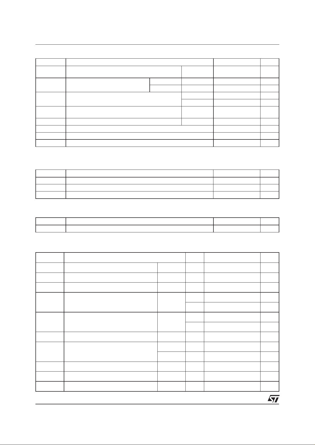
QUAD AC LINE SWITCH ARRAY
MAIN APPLICATIONS
AC Line switch for appliance control systems
n
Drive of low power high inductive or resistive
n
loads like:
- solenoid, relay, valve, dispenser
- micro-motor
- door lock
- low power lamp bulb
- pump
- fan
FEATURES
4 high voltage AC switch array
n
V
n
DRM/VRRM
Avalanche controlled device
n
I
n
T(RMS)
I
n
n
n
) = 0.4 A for the total array
T(RMS
Gate triggering current : IGT<10mA
Switch integrated driver
= 500V
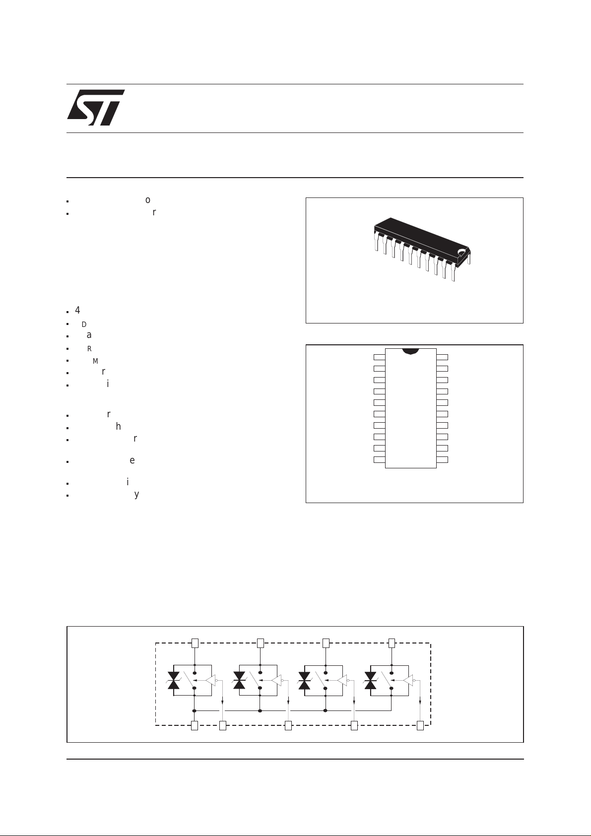
PIN OUT CONNECTION
= 0.2 A per switch
OUT1
OUT2
BENEFITS
n
Miniaturizes 4 switches in 1 package.
n
Reducestheswitchcomponentcountbyupto80%.
n
Needs no more external protection snubber &
OUT3
OUT4
varistor.
n
Enables the equipment to meet IEC1000-4-5
standard.
n
Interfaces directly with the microcontroller.
n
Eliminates any stressing gate kick back on the
note : pins 1, 3, 5, 7, 9, 12, 14, 16, 18, 20 not connected.
microcontroller.
DESCRIPTION
The ACS402belongstotheAClineswitchesarray
family built around the ASD™ concept. This high
performance planar technology device includes 4
bi-directional a.c. switches able to control an 0.2 A
resistive or inductive load.
Each ACS™ switch integrates a high voltage
clamping structure to absorb the inductive turn off
energy and a gate level shifter driver to separate
the digital controller from each main switch. It is
triggered with a negative gate current flowing out
of the gate pin.
Note:
For further technical information, please refer to the Application note AN1172
DIL20
1
G1
G2
G3
G4
COMCOM
FUNCTIONAL DIAGRAM
ACS402
D1
November 1999 - Ed: 3B
S1
Com
OUT1
ON
D2
G1 G2 G3 G4
OUT2
S2
ON
D3
OUT3
S3
ON
S4
D4
OUT4
ON
1/6
Page 2
ACS402-5SB4
ABSOLUTE RATINGS (limiting values)
Symbol Parameter Value Unit
V
DRM
V
RRM
I
T(RMS)
I
TSM
dI/dt Critical rate of rise of on-state current
V
PP
Tstg Storage temperature range - 40 to + 150 °C
Tj Operating junction temperature range 0 to + 110 °C
Tl Maximum lead temperature for soldering during 10s 260 °C
note 1 : according to test described by IEC 1000-4-5 standard & Figure 3.
SWITCH GATE CHARACTERISTICS (maximum values)
Symbol Parameter Value Unit
P
G (AV)
I
GM
V
GM
Repetitive peak off-state voltage Tj = 25 °C 500 V
RMS on-state current full cycle sine
wave 50 to 60 Hz
Non repetitive surge peak on-state current
Tj initial = 25°C, full cycle sine wave
= 20mA with tr = 100ns
I
G
Non repetitive line peak pulse voltage
per switch Tamb = 90 °C 0.2 A
total array Tamb = 75 °C 0.4 A
F =50 Hz 5 A
F =60 Hz 5.5 A
Repetitive
20 A/µs
F =120 Hz
note 1
2kV
Average gate power dissipation 0.1 W
Peak gate current (tp = 20µs) 1 A
Peak positive gate voltage (respect to the pin COM) 5 V
THERMAL RESISTANCE
Symbol Parameter Value Unit
Rth (j-a) Junction to ambient 90 °C/W
ELECTRICAL CHARACTERISTICS PER SWITCH
For either positive or negative polarity of pin OUT1, OUT2, OUT3, OUT4 voltage respect to pin COM voltage
Symbol Test conditions Values Unit
I
V
V
V
I
DRM
I
RRM
GT
I
I
GT
GD
H
L
TM
VD= 12V (DC) RL= 140Ω Tj=25°C MAX 10 mA
VD= 12V (DC) RL= 140Ω Tj=25°C MAX 1 V
V
OUT=VDRMRL
I
= 100mA gate open Tj=25°C TYP 25 mA
OUT
= 3.3kΩ Tj=110°C MIN 0.2 V
MAX 60 mA
IG= 20mA Tj=25°C TYP 30 mA
MAX 65 mA
I
= 0.3A tp= 380µs Tj=25°C MAX 1.1 V
OUT
V
OUT=VDRM
V
OUT=VRRM
Tj=25°C MAX 2 µA
Tj=110°C MAX 50 µA
dV/dt V
(dI/dt)c (dV
V
CL
2/6
= 400V gate open Tj=110°C MIN 500 V/µs
OUT
/dt)c = 10V/µs Tj=110°C MIN 0.1 A/ms
OUT
ICL= 1mA tp = 1ms Tj=25°C TYP 600 V
Page 3

ACS402-5SB4
AC LINE SWITCH BASIC APPLICATION
The ACS402 device is well adapted to washing machine, dishwasher, tumble drier, refrigerator, water
heater and cookware. It has been designed especially to switch ON and OFF low power loads such as solenoid, valve, relay, micro-motor, pump, fan, door lock and low wattage lamp bulb.
Pin COM: Common drive reference to connect to the power line neutral
Pin G: Switch Gate input to connect to the digital controller
Pin OUT: Switch Output to connect to the load
Each ACS™ switch is triggered with a negative gate current flowing out of the gate pin G. It can be driven
directly by the digital controller through a resistor as shown on the typical application diagram. Note that no
protection device (zener or capacitors) should be added between gates and common terminals.
In appliances systems, this ACS™ switch intends to drive low power load in full cycle ON / OFF mode. The
turn off commutation characteristics of these loads can be classified in 3 groups as shown in table 1.
Thanks to its thermal and turn off commutation performances, each switch of the ACS402 is able to drive
an inductive or resistive load up to 0.2 A with no additional turn off snubber.
Table 1: Load grouping versus their turn off commutation requirement (230V AC applications).
LOAD
IRMS
(A)
POWER
(dI/dt)c
FACTOR
(A/ms)
(dV/dt)c
(V/µs)
TURN-OFF
DELAY
Door lock Lamp < 0.3 1 0.15 0.15 < 10
< 0.6 1 0.4 0.15 < 20
Relay Valve
< 0.1 > 0.7 < 0.05 < 5 < 10
Dispenser
Micro-motor
Pump Fan < 0.2 > 0.2 < 0.1 < 10 < 10
< 0.6 > 0.2 < 0.3 < 10 < 20
TYPICAL APPLICATION DIAGRAM
VALVE / DISPENSER DOOR LOCK RELAY PUMP/FAN
L
MAINS
N
OUT1
S1
OUT2
S2
OUT3
S3
M
OUT4
ACS402
S4
(ms)
D1
COM
ON
G1 G2 G3 G4
PA0
Vcc
ON
D2
PA1 PA3PA2
Vss
ST72 MCU
ON
D3
D4
ON
3/6
Page 4

ACS402-5SB4
SWITCH-OFF OPERATION
At the end of the last conduction half-cycle, the load current reaches the holding current level IH, and the
ACS™ switch turns off. Because of the inductance L of the load, the current flows through the avalanche
diode D and decreases linearly to zero. During this time, the voltage across the switch is limited to the
clamping voltage V
Theenergy stored in the inductanceof the loaddepends on theholding current I
10H); it can reach about 20 mJ and is dissipated inthe clamping section that is especiallydesigned for that
purpose.
CL
.
andthe inductance (up to
H
Fig 1: Turn-off operation of the ACS402 switch
Fig 2: ACS402 switch static characteristic.
with an electro valve: waveform of the gatecurrent
, pin OUT current I
I
G
(10 mA/div)
I
H
V
OUT
(200V/div)
I
OUT
& voltage V
OUT
.
OUT
VCL= 650V
ime (400µs/div)
T
I
OUT
I
H
V
OUT
V
CL
AC LINE TRANSIENT VOLTAGE RUGGEDNESS
Each ACS402 switch is able to sustain safely the AC line transient voltages either by clamping the low energy spikes or by breaking over under high energy shocks, even with high turn-on current rises.
The test circuit of the figure 3 isrepresentative ofthe final ACS™ application andis alsoused to stress the
ACS™ switch according to the IEC1000-4-5 standard conditions. Thanks to the load, the ACS™ switch
sustainsthe voltage spikesup to 2kV above the peak line voltage. Itwill break oversafely even onresistive
load where the turn on current rise is high as shown on figure 4. Such non repetitive test can be done 10
times on each AC line voltage polarity.
Fig 3: Overvoltage ruggedness test circuit for
resistive and inductive loads according to IEC
1000-4-5 standard.
R = 150Ω,L=5µH, V
PP
= 2kV.
RL
AC LINE &
SURGE VOLTAGE
GENERATOR
4/6
VAC+V
PP
OUT
ACSxx
S
ON
D
GCOM
G
R
= 220
Ω
Fig 4: Current and voltage of the ACS™ during
IEC 1000-4-5 standard test with a 220Ω -10µH
load & V
= 2kV.
PP
Vout (200 V/div)
Iout (2 A/div)
dI/dt = 100 A/µs
Page 5

ACS402-5SB4
Fig 5: Relative variation of gate trigger current
versus junction temperature
IGT[Tj]/IGT[Tj=25°C]
2.00
1.75
1.50
1.25
1.00
0.75
0.50
0.25
0.00
0 25 50 75 100 125
Tj(°C)
Fig 7: On state characteristics @Tj max
=0.90 V & RT=0.3 Ω (maximum values)
V
TO
Pon V I R x I
=+.. .
22
TO T RMS T T RMS
IOUT (A)
5
2
1
0.8
0.6
0.5
0.4
0.3
0.2
0.1
0.07
0.05
0.5 0.75 1 1.25 1.5 1.75 2
() ()
Π
VTM (V)
2
Fig 6: Relative variation of holding & latching
currents versus junction temperature
IH[Tj]/IH[Tj=25°C] & IL [T j]/IL [T j= 2 5 ° C ]
2.0
1.8
1.6
1.4
1.2
1.0
0.8
0.6
0.4
0.2
0.0
0 25 50 75 100 125
Tj(°C)
Fig 8: Maximum total RMS current versus ambient
temperature on an inductive load (PF>0.1) and a
low repetitive rate (F<1Hz)
0.7
0.6
Total
Maximum
RMS current
0.5
0.4
(A)
0.3
0.2
0.1
0
0 20 40 60 80 100 120
AmbientTemperature (°C)
Fig 9: Relative variation of thermal impedance
junction to ambient versus pulse duration (epoxy
printed circuit board FR4, 35µm copper layout
thickness).
Zth(j-a)/Rth(j-a)
1E+0
1E-1
1 switch
1E-2
1E-3
1E-4 1E-3 1E-2 1E-1 1E+0 1E+1 1E+2 5E+2
4 switches
tp (s)
5/6
Page 6

ACS402-5SB4
ORDERING INFORMATION
ACS 4 02 - 5 S B 4
TM
C Switch
A
PACKAGE MECHANICAL DATA
DIL20 Plastic
a1
b
Z
20
B
e3
D
e
11
101
Number
of
Switch
I
L
I
TRMS
02 = 0.2A
F
E
V
DRM
5 = 500V
DIL
plastic
20 pins
Gate
Sensitivity
S = 10mA
DIMENSIONS
REF.
Millimeters Inches
Min. Typ. Max. Min. Typ. Max.
a1 0.38 0.015
B 1.40 1.65 0.055 0.065
b 0.45 0.018
b1
b1 0.25 0.010
D 26.3 1.035
E 10.90 0.430
e 2.54 0.100
e3 22.86 0.900
F 6.6 0.260
I 4.32 0.170
L 3.3 0.130
Z 1.84 0.072
Ordering type Marking Package Weight Base qty Delivery mode
ACS402-5SB4 ACS4025 DIL20 1.4g. 19 Tube
n
Epoxy meets UL94,V0
TM: ASD and ACS are trademarks of STMicroelectronics .
Informationfurnishedisbelievedtobeaccurateandreliable.However,STMicroelectronicsassumesnoresponsibilityfortheconsequencesof
useofsuch information nor for any infringement of patents or other rights of third parties which may result from its use. No license is granted by
implication or otherwise under any patent or patent rights of STMicroelectronics. Specifications mentioned in this publication are subject to
change without notice. This publication supersedes and replaces all information previously supplied.
STMicroelectronics products are not authorized for use as critical components in life support devices or systems without express written approval of STMicroelectronics.
The ST logo is a registered trademark of STMicroelectronics
© 1999 STMicroelectronics - Printed in Italy - All rights reserved.
Australia - Brazil - China - Finland - France - Germany - Hong Kong - India - Italy - Japan - Malaysia
Malta - Morocco - Singapore - Spain - Sweden - Switzerland - United Kingdom - U.S.A.
STMicroelectronics GROUP OF COMPANIES
http://www.st.com
6/6
 Loading...