

Page 1
®
ASD™
AC Switch Family
MAIN APPLICATIONS
AC on-off static switching in appliance control
n
systems
Drive of low power high inductive or resistive
n
loads like
- relay, valve, solenoid, dispenser
- pump, fan, micro-motor
- low power lamp bulb, door lock
FEATURES
Blocking voltage : V
n
Clamping voltage : VCL= 600 V
n
Nominal current : I
n
Gate triggering current : IGT<5mA
n
Switch integrated driver
n
n
SO-8 package:
DRM/VRRM
= 0.2 A
T(RMS)
- drivereferenceCOMconnectedto 2 coolingpins
- 3 mm creepage distance from pin OUT to other pins
BENEFITS
n
Needs no more external protection snubber or
varistor
n
Enables equipment to meet IEC 1000-4-5 &
IEC 335-1
n
Reduces component count by up to 80 %
n
Interfaces directly with a microcontroller
n
Eliminates any stressing gate kick back on
microcontroller
n
Allows straightforward connection of several
ACS on same cooling pad
= 500V
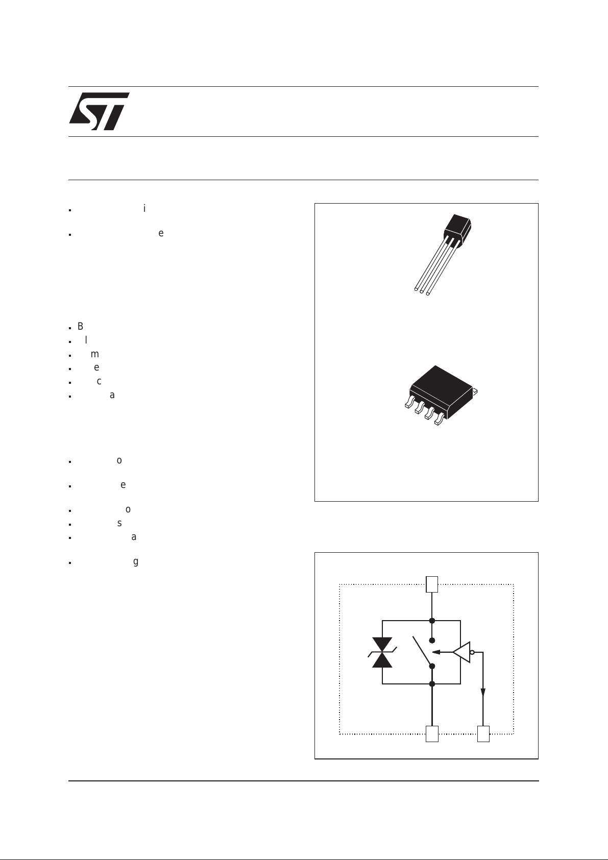
ACS102-5Tx
AC LINE SWITCH
PRELIMINARY DATASHEET
OUT
G
TO92
ACS102-5TA
NC
OUT
NC
ACS102-5T1
NC: Not Connected
FUNCTIONAL DIAGRAM
COM
NC
SO-8
NC
OUT
COM
COM
G
DESCRIPTION
The ACS102 belongs to the AC line switch family
built around the ASD concept. This high performance 5 mA switch circuit is able to control an up
to 0.3 A load.
The ACS switch embeds a high voltage clamping
structure to absorb the inductive turn off energy
anda gate levelshifter driver to separatethe digital
controller from the main switch. It is triggered with
anegative gate currentflowing out of thegate pin.
December 1999 - Ed: 4B
ACS102
D
S
COM
ON
G
1/8
Page 2
ACS102-5Tx
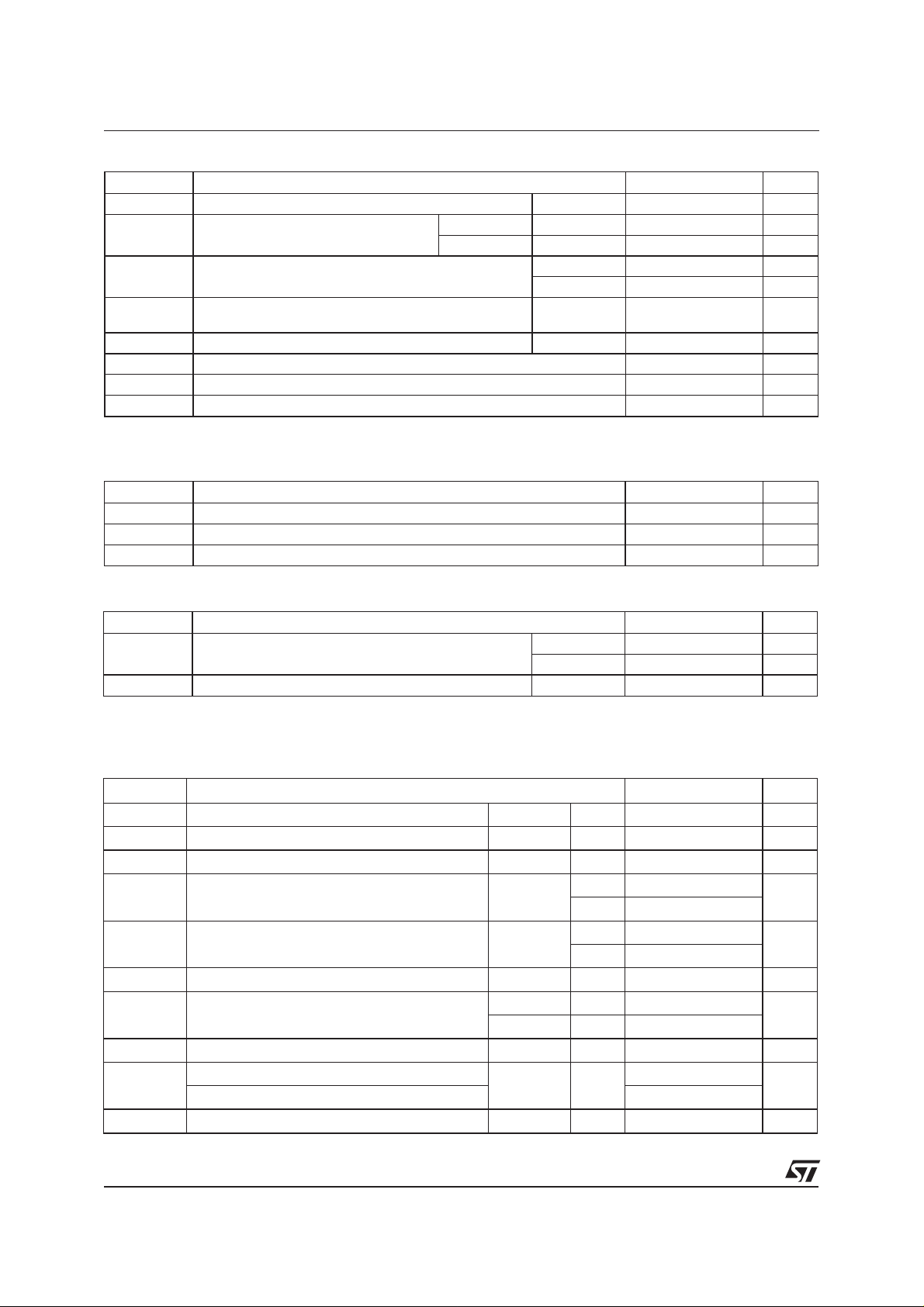
ABSOLUTE RATINGS (limiting values)
Symbol Parameter Value Unit
V
DRM/VRRM
I
T(RMS)
I
TSM
dI/dt Critical rate of rise of on-state current
V
PP
Tstg Storage temperature range - 40 to + 150 °C
Tj Operating junction temperature range 0 to + 110 °C
Tl Maximum lead temperature for soldering during 10s 260 °C
note 1 : according to test described by IEC 1000-4-5 standard & Figure 4.
SWITCH GATE CHARACTERISTICS (maximum values)
Symbol Parameter Value Unit
P
G (AV)
I
GM
V
GM
Repetitive peak off-state voltage Tj = 25 °C 500 V
RMS on-state current full cycle sine
wave 50 to 60 Hz
Non repetitive surge peak on-state current
Tj initial = 25°C, full cycle sine wave
TO92 Tamb = 75 °C 0.2 A
SO-8 Tamb = 75 °C 0.2 A
F =50 Hz 7.3 A
F =60 Hz 8 A
F =120 Hz 20 A/µs
= 10mA, tr = 100ns
I
G
Non repetitive line peak pulse voltage
note 1
2kV
Average gate power dissipation 0.1 W
Peak gate current (tp = 20µs) 1 A
Peak positive gate voltage (respect to the pin COM) 5 V
THERMAL RESISTANCES
Symbol Parameter Value Unit
Rth (j-a) Junction to ambient TO92 150 °C/W
SO-8 150 °C/W
Rth (j-l) Junction to leads for full AC line cycle conduction TO92 60 °C/W
ELECTRICAL CHARACTERISTICS
For either positive or negative polarity of pin OUT voltage respect to pin COM voltage
Symbol Test Conditions Values Unit
I
GT
V
GT
V
GD
I
H
I
L
V
TM
I
DRM
I
RRM
dV/dt V
(dI/dt)c Turn off = 10ms, (dV/dt)c = 5V/µs Tj=110°C MIN 0.1 A/ms
V
CL
tbd = to be defined
V
=12V (DC) RL=140Ω Tj=25°C MAX 5 mA
OUT
V
=12V (DC) RL=140Ω Tj=25°C MAX 0.9 V
OUT
V
OUT=VDRMRL
I
= 100mA gate open Tj=25°C TYP 20 mA
OUT
=3.3kΩ Tj=110°C MIN 0.2 V
MAX tbd
IG= 20mA Tj=25°C TYP 25 mA
MAX tbd
I
= 0.3A tp=380µs Tj=25°C MAX 1.2 V
OUT
V
OUT=VDRM
V
OUT=VRRM
=400V gate open Tj=110°C MIN 300 V/µs
OUT
Tj=25°C MAX 2 µA
Tj=110°C MAX 50
Turn off = 20ms, (dV/dt)c = 10V/µs 0.15
ICL= 1mA tp=1ms Tj=25°C TYP 600 V
2/8
Page 3
PARAMETER DESCRIPTION
Parameter Symbol Parameter Description
I
GT
Gate triggering current
ACS102-5Tx
V
GT
V
GD
I
H
I
L
V
TM
I
/ I
DRM
RRM
dV/dt Static pin OUT voltage rise
(dl/dt)
C
V
CL
Gate triggering voltage
Non triggering voltage
Holding current
Latching current
On state voltage
Forward or reverse leakage current
Turn off current rate of decay
Clamping voltage
AC LINE SWITCH BASIC APPLICATION
The ACS102 device is well adapted to washing machine, dish washer, tumble drier, refrigerator, water
heaters, and cookware. It has been designed especially to switch on & off low power loads such as solenoid, valve, relay, dispenser, micro-motor, pump, fan, door lock, and low wattage lamps bulbs.
PinCOM : Common drive reference to connect to the power line neutral
Pin G : Switch Gate input to connect to the digital controller through a resistor
Pin OUT : Switch Output to connect to the load
This ACS switch is triggered with a negative gate current flowing out of the gate pin G. It can be driven directly by the digital controller through a resistor as shown on the typical application diagram. No protection
device (zener or capacitor) are required between gate and COM terminals.
The SO-8 version allows to connect several ACS102 devices on the same cooling PCB pad which is the
COM pin.
In appliances systems, the ACS102 switch intends to drive low power load in full cycle ON / OFF mode.
The turn off commutation characteristics of these loads are described in table 1.
Thanks to its thermal and turn off commutation performances, the ACS102 switch is able to drive with no
turn off aid snubber a load up to 0.2 A (door lock, lamp, relay, valve & micro motor) when this load has to
switch off withinone half AC line cycle, and up to 0.3 A (pump, fan) when this load can switch off within one
full AC line cycle.
Table 1: Low power load turn off commutation requirement (230V AC applications).
IRMS
LOAD
(A)
Door lock, lamp < 0.2 1 < 0.1 < 0.15 < 10
Relay Valve
Dispenser
Micro-motor
Pump Fan < 0.3 > 0.2 < 0.15 <10 < 20
< 0.2 > 0.7 < 0.1 < 5 < 10
POWER
FACTOR
(dI/dt)c
(A/ms)
(dV/dt)c
(V/µs)
TURN-OFF
DELAY
(ms)
3/8
Page 4

ACS102-5Tx
TYPICAL APPLICATION DIAGRAM
COM
LOAD
L
R
OUT
S
ON
ACS102
G
L
MAINS
N
AC
D
ST 72 MCU
-Vcc
HIGH INDUCTIVE SWITCH-OFF OPERATION
At the end of the last conduction half-cycle, the load current reaches the holding current level I
, and the
H
ACS™ switch turns off. Because of the inductance L of the load, the current flows through the avalanche
diode D and decreases linearly to zero. During this time, the voltage across the switch is limited to the
clamping voltage V
The energy stored in the inductance of the load depends on the holding current I
CL
.
and the inductance (up
H
to10 H); it canreach about 20mJ and is dissipatedin the clampingdiode section. The ACSswitch sustains
the turn off energy , because its clamping section is designed for that purpose.
Fig 1: Turn-off operation of the ACS102 switch
with an electro valve: waveform of the gatecurrent
, pin OUT current I
I
G
(10 mA/div)
H
I
OUT
V
(200V/div)
4/8
OUT
I
& voltage V
OUT
.
OUT
VCL = 650V
ime (400µs/div)
T
Fig 2: ACS102 switch static characteristic.
I
OUT
I
H
V
CL
V
OUT
Page 5

ACS102-5Tx
AC LINE TRANSIENT VOLTAGE RUGGEDNESS
The ACS102 switch is able to sustain safely the AC line transient voltages either by clamping the low energyspikes or bybreaking over underhigh energy shocks,even withhigh turn-on currentrates of increase.
The test circuit of the figure 3 is representative of the final ACS application and is also used to stress the
ACS switch according to the IEC1000-4-5 standard conditions. Thanks to the load, the ACS switch sustains the voltage spikes up to 2 kV above the peak line voltage. It will breaks over safely even on resistive
loadwhere the turn on current rate of increase ishigh as shown on figure 4. Such non repetitivetest can be
done 10 times on each AC line voltage polarity.
Fig. 3: Overvoltage ruggedness testcircuit for
resistive and inductive loads according to
IEC 1000-4-5 standard.
R = 150Ω,L=5µH, V
PP
= 2kV.
RL
AC LINE &
SURGE VOLTAGE
GENERATOR
VAC+V
PP
OUT
ACSxx
S
ON
D
GCOM
RG= 220
Ω
Fig 5: Relative variation of gate trigger current
versus junction temperature
IGT[Tj]/IGT[Tj=25°C]
2.00
1.75
1.50
1.25
1.00
0.75
0.50
0.25
0.00
0 25 50 75 100 125
Tj(°C)
Fig. 4: Current and Voltage of the ACS during
IEC 1000-4-5 standard test withR=150Ω,L=
5µH & V
= 2kV.
PP
Vout (200V/div)
Iout (2.5 A/div)
dI/dt = 70 A/µs
Fig 6: Relative variation of holding & latching
currents versus junction temperature
IH[Tj]/IH[Tj=25°C] & IL [Tj]/IL[Tj=25°C]
2.0
1.8
1.6
1.4
1.2
1.0
0.8
0.6
0.4
0.2
0.0
0 25 50 75 100 125
Tj(°C)
5/8
Page 6

ACS102-5Tx
Fig 7: Typical on state characteristics @ Tj max
=0.85V&RT= 0.40 Ω (maximum values)
V
TO
Pon V I R x I
=+.. .
22
TO T RMS T T RMS
Iout_m (A)
2
1
0.8
0.6
0.5
0.4
0.3
0.2
0.1
0.07
0.05
0.75 1 1.25 1.5
() ()
Π
Von (V)
2
Fig. 9-1: Relative variation of the junction to
ambient thermal impedance versus conducting
pulse duration for the SO8. Standard foot print
with 35µm copper layout thickness.
Fig 8: Maximum RMS switch current versus
ambient temperature on inductive load (PF>0.1)
and a low repetitive rate (F < 0.1 Hz) for both TO92
and SO8.
IT(RMS) (A)
0.4
0.3
0.2
0.1
0
0 10 20 30 40 50 60 70 80 90 100 110 120
Full cycle turn off delay Half cycle turn-off delay
Tamb (°C)
Fig. 9-2: Relative variation of the junction to
ambient thermal impedance versus conducting
pulse duration for the TO92.
Zth (j-a) / Rth (j-a)
1
0.1
0.01
0.001 0.01 0.1 1 10 100
tp (s)
ORDERING INFORMATION
ACS 1 02 - 5 T X
TRMS
AC
Switch
Number
of
Switch
I
02 = 0.2 A
Zth (j-a) / Rth (j-a)
1
0.1
Gate
tp (s)
A = TO 92
1 = SO-8
0.01
0.001 0.01 0.1 1 10 100
DRM
V
5 = 500V
sensistivity
T = 5 mA
6/8
Page 7

PACKAGE OUTLINE MECHANICAL DATA
SO-8
L
A
a2
b
8
1
e
e3
D
M
5
4
S
F
c1
C
a
1
E
ACS102-5Tx
DIMENSIONS
REF.
a3
A 1.75 0.069
b
1
a1 0.1 0.25 0.004 0.010
a2 1.65 0.065
a3 0.65 0.85 0.025 0.033
b 0.35 0.48 0.014 0.019
b1 0.19 0.25 0.007 0.010
C 0.25 0.50 0.50 0.010 0.020
c1 45° (typ)
D 4.8 5.0 0.189 0.197
E 5.8 6.2 0.228 0.244
Millimetres Inches
Min. Typ. Max. Min. Typ. Max.
PACKAGE FOOT PRINT
SO-8
6.8
4.2
e 1.27 0.050
e3 3.81 0.150
F 3.8 4.0 0.15 0.157
L 0.4 1.27 0.016 0.050
M 0.6 0.024
S 8°(max)
0.6
1.27
7/8
Page 8

ACS102-5Tx
PACKAGE OUTLINE MECHANICAL DATA
TO92 Plastic
DIMENSIONS
REF.
a
A 1.35 0.053
BAC
B 4.70 0.185
C 2.54 0.100
D 4.40 0.173
F
D
E
E 12.70 0.500
F 3.70 0.146
a 0.45 0.017
Ordering type Marking Package Weight Base qty Delivery mode
ACS102-5TA ACS102 TO92 0.2g 2500 Bulk
ACS102-5TA-TR ACS102 TO92 0.2g 2000 Tape & reel
ACS102-5T1-TR ACS102 SO-8 0.11g 2500 Tape & reel
Millimeters Inches
Min. Typ. Max. Min. Typ. Max.
TM: ASD and ACS are trademarks of STMicroelectronics .
Informationfurnishedis believed to be accurate and reliable. However, STMicroelectronics assumesnoresponsibility for the consequences of
useof such information nor for any infringement ofpatents or other rights of third parties which mayresult from its use. No license is grantedby
implication or otherwise under any patent or patent rights of STMicroelectronics. Specifications mentioned in this publication are subject to
change without notice. This publication supersedes and replaces all information previously supplied.
STMicroelectronics products are not authorized for use as critical components in life support devices or systems without express written approval of STMicroelectronics.
The ST logo is a registered trademark of STMicroelectronics
© 1999 STMicroelectronics - Printed in Italy - All rights reserved.
Australia - Brazil - China - Finland - France - Germany - Hong Kong - India - Italy - Japan - Malaysia
Malta - Morocco - Singapore - Spain - Sweden - Switzerland - United Kingdom - U.S.A.
STMicroelectronics GROUP OF COMPANIES
http://www.st.com
8/8
 Loading...