

Page 1
ACPL-W60L/K63L
High Speed LVTTL Compa tible
3.3 V olt Optocouplers
Data Sheet
Description
The ACPL-W60L/K63L are optically coupled gates
that combine a GaAsP light emitting diode and an
integrated high gain photo detector. The output of the
detector IC is an open collector Schottky-clamped
transistor. The internal shield provides a guaranteed
common mode transient immunity specification of 15
kV/µs.
This unique design provides maximum AC and DC
circuit isolation while achieving LVTTL/LVCMOS
compatibility. The optocoupler AC and DC operational
parameters are guaranteed from –40˚C to +85˚C
allowing trouble-free system performance.
Applications
• Isolated line receiver
• Computer-peripheral interfaces
• Microprocessor system interfaces
• Digital isolation for A/D, D/A conversion
• Switching power supply
• Instrument input/output isolation
• Ground loop elimination
• Pulse transformer replacement
• Fieldbus
CATHODE
Features
• Package clearance/creepage at 8 mm
• Low power consumption
• 15 kV/µs minimum Common Mode Rejection (CMR) at
VCM = 50 V
• High speed: 15 MBd typical
• LVTTL/LVCMOS compatible
• Low input current capability: 5 mA
• Guaranteed AC and DC performance over temperature:
–40˚C to +85˚C
• Available in 6-pin stretched SO-6 and 8 pin stretched
SO-8
• Safety approvals: UL, CSA, IEC/EN/DIN EN 60747-5-2 –
in process
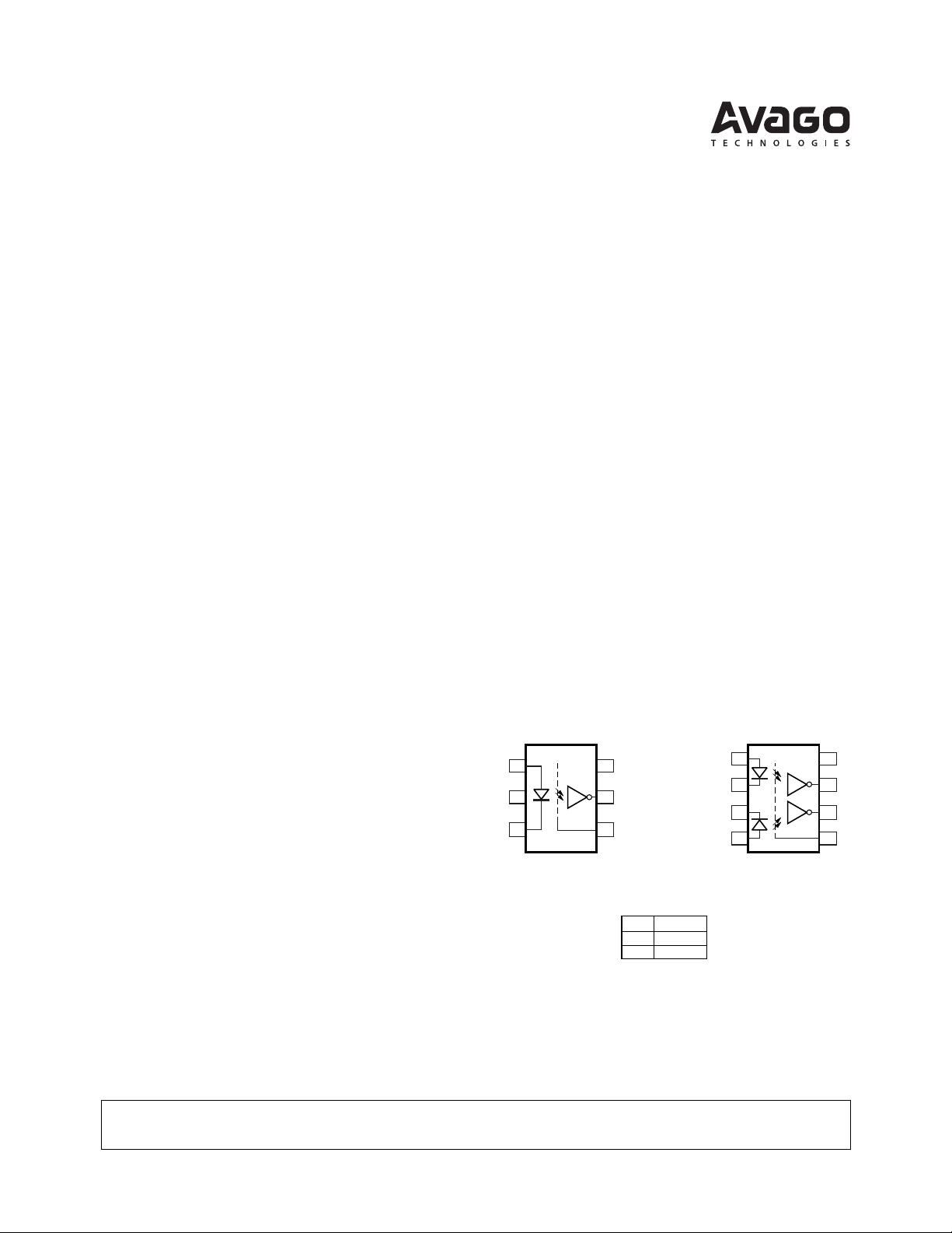
Functional Diagram
ANODE
ACPL-W60L
1
2
3
SHIELD
V
6
CC
5
V
O
GND
4
ANODE
CATHODE
CATHODE
ANODE
1
1
2
2
ACPL-K63L
1
2
3
4
SHIELD
*
V
8
CC
V
7
O1
V
6
O2
GND
5
TRUTH TABLE
(POSITIVE LOGIC)
LED
OUTPUT
ON
OFF
L
H
*Advanced Information
A 0.1 µF bypass capacitor must be
connected between pins 5 and 8.
CAUTION: It is advised that normal static precautions be taken in handling and assembly of this component to prevent
damage and/or degradation which may be induced by ESD.
Page 2
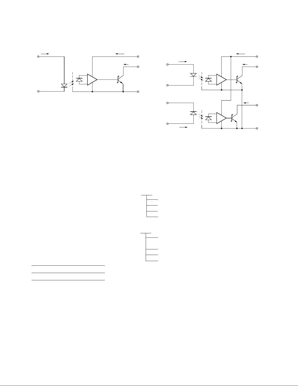
Schematic Diagrams
I
F
1+
V
F
–
3
USE OF A 0.1 µF BYPASS CAPACITOR CONNECTED
BETWEEN PINS 5 AND 8 IS RECOMMENDED (SEE NOTE 5).
These optocouplers are suitable
for high speed logic interfacing,
ACPL-W60L
SHIELD
Ordering Information
Specify Part Number followed by Option Number (if desired).
input/output buffering, as line
receivers in environments that
conventional line receivers
Example:
ACPL-W60L -XXXX
cannot tolerate and are
recommended for use in
extremely high ground or induced
noise environments.
Example:
These optocouplers are available
ACPL-K63L -XXXX*
in stretched SO-6 and SO-8
package. The part numbers are as
follows:
Package
ACPL-W60L Stretched SO-6
ACPL-K63L Stretched SO-8
Option data sheets available. Contact Avago sales representative or
authorized distributor for information.
I
CC
V
CC
6
I
O
V
O
5
GND
4
I
F1
1
+
V
F1
–
2
3
–
V
F2
+
I
4
F2
ACPL-K63L
SHIELD
SHIELD
I
CC
V
CC
8
I
O1
V
O1
7
I
O2
V
O2
6
GND
5
020 = UL5000 Vrms/minute Option
060 = IEC/EN/DIN EN 60747-5-2
500 = Tape and Reel Packaging Option
XXXE = Lead Free Option
020 = UL5000 Vrms/minute Option – pending
qualification
060 = IEC/EN/DIN EN 60747-5-2
500 = Tape and Reel Packaging Option
XXXE = Lead Free Option
2
Page 3

Package Outline Drawings
ACPL-W60L Stretched SO-6 Package
0.381 ± 0.127
(0.015 ± 0.005)
0.45 (0.018)
1
2
3
6.807
0.268
(
7°
45°
1.27 (0.050) BSG
+0.127
0
+0.005
)
-0.000
6
5
4
1.590 ± 0.127
(0.063 ± 0.005)
4.580
0.180
(
+0.254
0
+0.010
-0.000
LAND PATTERN RECOMMENDATION
12.65 (0.498)
0.76 (0.030)
)
1.91 (0.075)
7°
0.20 ± 0.10
(0.008 ± 0.004)
0.750 ± 0.250
(0.0295 ± 0.010)
11.50 ± 0.250
(0.453 ± 0.010)
ACPL-K63L Stretched SO-8 Package
0.381 ± 0.13
(0.015 ± 0.005)
1
2
3
4
1.270 (0.050) BSG
8
7
6
5
3.180 ± 0.127
(0.125 ± 0.005)
+0.25
5.850
0
+0.010
0.230
(
-0.000
DIMENSIONS IN MILLIMETERS (INCHES).
LEAD COPLANARITY = 0.1 mm (0.004 INCHES).
LAND PATTERN RECOMMENDATION
12.650 (0.5)
)
0.450 (0.018)
0.200 ± 0.100
(0.008 ± 0.004)
0.750 ± 0.250
(0.0295 ± 0.010)
3
1.590 ± 0.127
7°
45°
6.807 ± 0.127
(0.268 ± 0.005)
11.5 ± 0.250
(0.453 ± 0.010)
(0.063 ± 0.005)
3.180 ± 0.127
(0.125 ± 0.005)
7°
DIMENSIONS IN MILLIMETERS (INCHES).
LEAD COPLANARITY = 0.1 mm (0.004 INCHES).
1.905 (0.1)
Page 4
Recommended Solder Reflow Thermal Profile
300
PREHEATING RATE 3°C + 1°C/–0.5°C/SEC.
REFLOW HEATING RATE 2.5°C ± 0.5°C/SEC.
ROOM
TEMPERATURE
200
160°C
150°C
140°C
100
TEMPERATURE (°C)
0
0
50 150100 200 250
2.5°C ± 0.5°C/SEC.
3°C + 1°C/–0.5°C
PREHEATING TIME
150°C, 90 + 30 SEC.
TIME (SECONDS)
Note:
Use of non chlorine-activated fluxes is highly recommended.
Recommended PB-Free IR Profile
PEAK
TEMP.
245°C
30
SEC.
SEC.
30
SOLDERING
TIME
200°C
50 SEC.
PEAK
TEMP.
240°C
PEAK
TEMP.
230°C
TIGHT
TYPICAL
LOOSE
T
p
217 °C
T
L
150 - 200 °C
T
smax
T
smin
TEMPERATURE
25
NOTES:
THE TIME FROM 25 °C to PEAK TEMPERATURE = 8 MINUTES MAX.
T
= 200 °C, T
smax
t 25 °C to PEAK
260 +0/-5 °C
RAMP-UP
3 °C/SEC. MAX.
t
s
PREHEAT
60 to 180 SEC.
= 150 °C
smin
TIME
Note:
Use of non chlorine-activated fluxes is highly recommended.
Regulatory Information
The ACPL-W60L//K63L have
been approved by the following
organizations:
UL - Pending
Approval under UL 1577,
Component Recognition
Program, File E55361.
TIME WITHIN 5 °C of A CTUAL
PEAK TEMPERATURE
t
p
20-40 SEC.
RAMP-DOWN
6 °C/SEC. MAX.
t
L
60 to 150 SEC.
CSA - Pending
Approval under CSA Component
Acceptance Notice #5, File CA
88324.
IEC/EN/DIN EN 60747-5-2 - Pending
Approved under:
IEC 60747-5-2:1997 + A1:2002
EN 60747-5-2:2001 + A1:2002
DIN EN 60747-5-2 (VDE 0884
Teil 2):2003-01
(Option 060 only)
4
Page 5

Insulation and Safety Related Specifications
Stretched
SO-6 and SO-8
Parameter Symbol Value Units Conditions
Minimum External Air L (101) 8 mm Measured from input terminals to output
Gap (External Clearance) terminals, shortest distance through air.
Minimum External Tracking L (102) 8 mm Measured from input terminals to output
(External Creepage) terminals, shortest distance path along body.
Minimum Internal Plastic 0.08 mm Through insulation distance, conductor to
Gap (Internal Clearance) conductor, usually the direct distance
between the photoemitter and photodetector
inside the optocoupler cavity.
Tracking Resistance CTI 175 Volts DIN IEC 112/VDE 0303 Part 1
(Comparative Tracking
Index)
Isolation Group IIIa Material Group (DIN VDE 0110, 1/89, Table 1)
IEC/EN/DIN EN 60747-5-2 Insulation Related Characteristics
Description Symbol Stretched S0-6 & SO-8 Value Units
Installation classification per DIN VDE 0110/1.89, Table 1
for rated mains voltage ≤ 150 V rms I-IV
for rated mains voltage ≤ 300 V rms I-III
for rated mains voltage ≤ 600 V rms I-II
Climatic Classification 55/100/21
Pollution Degree (DIN VDE 0110/1.89) 2
Maximum Working Insulation Voltage V
IORM
630 V
peak
Input to Output Test Voltage, Method b*
V
x 1.875 = VPR, 100% Production Test V
IORM
PR
1181 V
peak
with tm = 1 sec, Partial Discharge < 5 pC
Input to Output Test Voltage, Method a*
V
x 1.5 = VPR, Type and Sample Test, V
IORM
PR
945 V
peak
tm = 60 sec, Partial Discharge < 5 pC
Highest Allowable Overvoltage* V
(Transient Overvoltage, t
= 10 sec)
ini
IOTM
6000 V
peak
Safety Limiting Values
Case Temperature T
Input Current I
Output Power P
Insulation Resistance at TS, VIO = 500 V R
S
S,INPUT
S,OUTPUT
S
175 ˚C
230 mA
600 mW
≥ 109Ω
*Refer to the front of the optocoupler section of the current catalog, under Product Safety Regulations section IEC/EN/DIN EN 60747-5-2, for a detailed
description.
Note: Isolation characteristics are guaranteed only within the safety maximum ratings which must be ensured by protective circuits in application.
5
Page 6

Absolute Maximum Ratings (No Derating Required up to 85˚C)
Parameter Symbol Package** Min. Max. Units Note
Storage Temperature T
Operating Temperature† T
Average Forward Input Current I
S
A
F
Single Stretched 20 mA 2
–55 125 ˚C
–40 85 ˚C
SO-6
Dual Stretched 15 1, 3
SO-8
Reverse Input Voltage V
Input Power Dissipation P
Supply Voltage (1 Minute Maximum) V
Output Collector Current I
Output Collector Voltage V
Output Power Dissipation P
R
I
CC
O
O
O
Single Stretched 85 mW
5V1
40 mW
7V
50 mA 1
7V1
SO-6
Dual Stretched 60 1, 4
SO-8
Solder Reflow Temperature Profile See Package Outline Drawings
section
**Ratings apply to all devices except otherwise noted in the Package column.
Recommended Operating Conditions
Parameter Symbol Min. Max. Units
Input Current, Low Level IFL*0 250 µA
[1]
[1]
IFH** 5 15 mA
CC
A
2.7 3.6 V
–40 85 ˚ C
N5TTL Loads
L
330 4 k Ω
Input Current, High Level
Power Supply Voltage V
Operating Temperature T
Fan Out (at RL = 1 kΩ)
Output Pull-up Resistor R
*The off condition can also be guaranteed by ensuring that VFL ≤ 0.8 volts.
**The initial switching threshold is 5 mA or less. It is recommended that 6.3 mA to 10 mA be used
for best performance and to permit at least a 20% LED degradation guardband.
6
Page 7

Electrical Specifications
Over Recommended Temperature (TA = –40˚C to +85˚C) unless otherwise specified. All Typicals at VCC = 3.3 V,
TA = 25˚C.
Parameter Sym. Device Min. Typ. Max. Units Test Conditions Fig. Note
High Level IOH*4.550µAVCC = 3.3 V, VO = 3.3 V, 1 1
Output Current IF = 250 µA
Input Threshold I
TH
3.0 5.0 mA VCC = 3.3 V, VO = 0.6 V, 2
Current IOL (Sinking) = 13 mA
Low Level VOL*0.350.6VV
= 3.3 V, 3
CC
Output Voltage IF = 5 mA,
IOL (Sinking) = 13 mA
High Level I
Supply Current
Low Level I
Supply Current
Input Forward V
CCH
CCL
F
Single 4.7 7.0 mA IF = 0 mA
Dual 6.9 10.0 VCC = 3.3 V
Single 7.0 10.0 mA IF = 10 mA
Dual 8.7 15.0 VCC = 3.3 V
1.41.5 1.75* V TA = 25˚C, IF = 10 mA 5 1
Voltage
Input Reverse BVR*5 VI
= 10 µA1
R
Breakdown
Voltage
Input Diode ∆VF/ –1.6 mV˚C IF = 10 mA 1
Temperature ∆T
A
Coefficient
Input C
IN
60 pF f = 1 MHz, VF = 0 V 1
Capacitance
7
Page 8

Switching Specifications
Over Recommended Temperature (TA = –40˚C to +85˚C), VCC = 3.3 V, IF = 7.5 mA unless otherwise specified. All Typicals
at TA = 25˚C, VCC = 3.3 V.
Parameter Sym. Min. Typ. Max. Units Test Conditions Fig. Note
Propagation Delay t
PLH
90 ns RL = 350 Ω 6, 7, 8 1, 6
Time to High Output CL = 15 pF
Level
Propagation Delay t
PHL
75 ns 1, 7
Time to Low Output
Level
Pulse Width |t
PHL
– t
|25ns 89
PLH
Distortion
Propagation Delay t
PSK
40 ns 8, 9
Skew
Output Rise Time t
r
45 ns 1
(10-90%)
Output Fall Time t
f
20 ns 1
(90-10%)
Parameter Sym. Device Min. Typ. Units Test Conditions Fig. Note
Logic High |CMH| ACPL-K63L 15,000 25,000 V/µs|VCM| = 10 V* VCC = 3.3 V, IF = 0 mA, 9 10, 12
Common ACPL-W60L 15,000 25,000 |VCM| = 1 KV V
O(MIN)
= 2 V,
Mode RL = 350 Ω, TA = 25˚C
Transient ACPL-K63L 15,000 25,000 |VCM| = 50 V*
Immunity ACPL-W60L 15,000 25,000 |VCM| = 1 KV
Logic Low |CML| ACPL-K63L 15,000 25,000 V/µs|VCM| = 10 V* VCC = 3.3 V, IF = 7.5 mA, 9 11, 12
Common ACPL-W60L 15,000 25,000 |VCM| = 1 KV V
O(MAX)
= 0.8 V,
Mode RL = 350 Ω, TA = 25˚C
Transient ACPL-K63L 15,000 25,000 |VCM| = 50 V*
Immunity ACPL-W60L 15,000 25,000 |VCM| = 1 KV
*Pending for higher VCM to 1 KV by 7 Aug 2006.
8
Page 9

Package Characteristics
All Typicals at TA = 25˚C.
Parameter Sym. Package Min. Typ. Max Units Test Conditions Fig. Not e
Input-Output I
Insulation V
Input-Output V
Momentary Dual Channel T
*Single 1 µA 45% RH, t = 5 s, 13, 14
I-O
= 3 kV DC, TA = 25˚C
I-O
Single, 3750 V rms RH ≤ 50%, t = 1 min, 13, 14
ISO
= 25˚C
A
Withstand
Voltage*
Input-Output R
Single, 10
I-O
12
Ω V
=500 V dc 1, 13, 15
I-O
Resistance Dual Channel
Input-Output C
Single, 0.5 pF f = 1 MHz, TA = 25˚C 1, 13, 15
I-O
Capacitance Dual Channel
Input-Input I
I-I
Insulation V
Dual Channel 0.005 µA RH ≤ 45%, t = 5 s, 16
= 500 V
I-I
Leakage
Current
Resistance R
Dual Channel 10
I-I
11
Ω 16
(Input-Input)
Capacitance C
Dual Channel 0.25 pG f = 1 MHz 16
I-I
(Input-Input)
*The Input-Output Momentary Withstand Voltage is a dielectric voltage rating that should not be interpreted as an input-output continuous voltage
rating. For the continuous voltage rating refer to the IEC/EN/DIN EN 60747-5-2 Insulation Characteristics Table (if applicable), your equipment
level safety specification or Avago Application Note 1074 entitled "Optocoupler Input-Output Endurance Voltage."
Notes:
1. Each channel.
2. Peaking circuits may produce transient input currents up to 50 mA, 50 ns maximum pulse width, provided average current does not
exceed 20 mA.
3. Peaking circuits may produce transient input currents up to 50 mA, 50 ns maximum pulse width, provided average current does not
exceed 15 mA.
4. Derate linearly above +80˚C free-air temperature at a rate of 2.7 mW/˚C.
5. Bypassing of the power supply line is required, with a 0.1 µF ceramic disc capacitor adjacent to each optocoupler as illustrated in
Figure 11. Total lead length between both ends of the capacitor and the isolator pins should not exceed 20 mm.
6. The t
7. The t
8. t
9. See test circuit for measurement details.
10. CMH is the maximum tolerable rate of rise on the common mode voltage to assure that the output will remain in a high logic state
11. CML is the maximum tolerable rate of fall of the common mode voltage to assure that the output will remain in a low logic state
12. For sinusoidal voltages, (|dV
13. Single channel device is considered a two-terminal part when pins 1, 2, 3 are shorted together, and pins 4, 5, 6 shorted together separately.
14. In accordance with UL 1577, each optocoupler is proof tested by applying an insulation test voltage ≥ 4500 V rms for one second (leakage
15. Measured between the LED anode and cathode shorted together and pins 5 through 8 shorted together. For dual channel products only.
16. Measured between pins 1 and 2 shorted together, and pins 3 and 4 shorted together. For dual channel products only.
propagation delay is measured from the 3.75 mA point on the falling edge of the input pulse to the 1.5 V point on the rising edge
PLH
of the output pulse.
propagation delay is measured from the 3.75 mA point on the rising edge of the input pulse to the 1.5 V point on the falling edge
PHL
of the output pulse.
is equal to the worst case difference in t
PSK
conditions.
(i.e., Vo > 2.0 V).
(i.e., Vo < 0.8 V).
Dual channel device is considered a two-terminal part when pins 1, 2, 3, 4 are shorted together, and pins 5, 6, 7, 8 are shorted together
separately.
detection current limit, I
IEC/EN/DIN EN 60747-5-2 Insulation Characteristics Table, if applicable.
| / dt)
CM
max
≤ 5 µA). This test is performed before the 100% production test for partial discharge (Method b) shown in the
I-O
and/or t
PHL
= πfCMVCM (p-p).
that will be seen between units at any given temperature and specified test
PLH
9
Page 10

15
V
= 3.3 V
CC
= 3.3 V
V
O
= 2.0 V*
V
E
= 250 µA
I
10
F
* FOR SINGLE
CHANNEL
PRODUCTS
ONLY
5
– HIGH LEVEL OUTPUT CURRENT – µA
0
-60
-40 0 40 80
OH
I
-20
20
60
TA – TEMPERATURE – °C
100
SINGLE STRETCHED SO-6
12
VCC = 3.3 V
V
= 0.6 V
O
10
8
RL = 350 KΩ
6
RL = 1 KΩ
4
2
– INPUT THRESHOLD CURRENT – mA
0
TH
I
-60 -20 20
T
– TEMPERATURE – °C
A
RL = 4 KΩ
60
SINGLE STRETCHED SO-6
0.8
0.7
VCC = 3.3 V
V
= 2.0 V*
E
I
= 5.0 mA
F
* FOR SINGLE
CHANNEL
PRODUCTS ONLY
0.6
0.5
0.4
0.3
IO = 13 mA
0.2
0.1
– LOW LEVEL OUTPUT VOLTAGE – V
0
100
80400-40
OL
-60 -20 20
V
– TEMPERATURE – °C
T
A
80400-40
100
60
Figure 1. Typical high level output current vs.
temperature.
70
VCC = 3.3 V
V
= 2.0 V*
E
V
= 0.6 V
OL
* FOR SINGLE
CHANNEL
PRODUCTS ONLY
60
50
IF = 5.0 mA
40
20
– LOW LEVEL OUTPUT CURRENT – mA
-60 -20 20
OL
I
T
A
– TEMPERATURE – °C
80400-40
60
Figure 4. Typical low level output current vs.
temperature.
SINGLE CHANNEL
I
INPUT
NODE
F
1
2
3
R
M
V
GND
CC
PULSE GEN.
Z = 50 Ω
O
t = t = 5 ns
f
r
MONITORING
6
5
4
Figure 2. Typical input threshold current vs.
temperature.
SINGLE STRETCHED SO-6
100
10
I
F
+
V
F
–
1.0
0.1
1.1
1.3
VF – FORWARD VOLTAGE – V
100
1000
0.01
– FORWARD CURRENT – mA
F
I
0.001
Figure 5. Typical input diode forward
characteristic.
3.3 V
0.1 µF
BYPASS
R
L
OUTPUT VO
L
MONITORING
NODE
*C
MONITORING
= 25 °C
T
A
PULSE GEN.
Z
= 50 Ω
O
t
= tr = 5 ns
f
INPUT
NODE
Figure 3. Typical low level output voltage vs.
temperature.
1.6
1.51.2 1.4
I
F
R
M
DUAL CHANNEL
1
2
3
4
V
GND
CC
8
7
6
5
0.1 µF
BYPASS
3.3 V
R
L
OUTPUT V
MONITORING
NODE
C
*
L
O
Figure 6. Test circuit for t
10
PHL
and t
PLH
IS APPROXIMATELY 15 pF WHICH INCLUDES
*C
L
PROBE AND STRAY WIRING CAPACITANCE.
INPUT
I
F
OUTPUT
V
t
PHL
O
t
PLH
IF = 7.50 mA
= 3.75 mA
I
F
1.5 V
.
Page 11

150
VCC = 3.3 V
I
= 7.5 mA
F
120
t
, RL = 350 Ω
90
PLH
60
t
, RL = 350 Ω
30
– PROPAGATION DELAY – ns
P
t
PHL
0
-60 -20 20
– TEMPERATURE – °C
T
A
50
40
VCC = 3.3 V
I
= 7.5 mA
F
30
20
RL = 350 Ω
10
0
PWD – PULSE WIDTH DISTORTION – ns
80400-40
100
60
-60
-20 20
– TEMPERATURE – °C
T
A
80400-40
100
60
Figure 7. Typical propagation delay vs.
temperature.
I
F
B
A
V
FF
SINGLE CHANNEL
1
2
3
+
PULSE
GENERATOR
Z
= 50 Ω
O
V
CM
–
V
CC
GND
Figure 8. Typical pulse width distortion vs.
temperature.
6
0.1 µF
BYPASS
5
4
V
CM
0 V
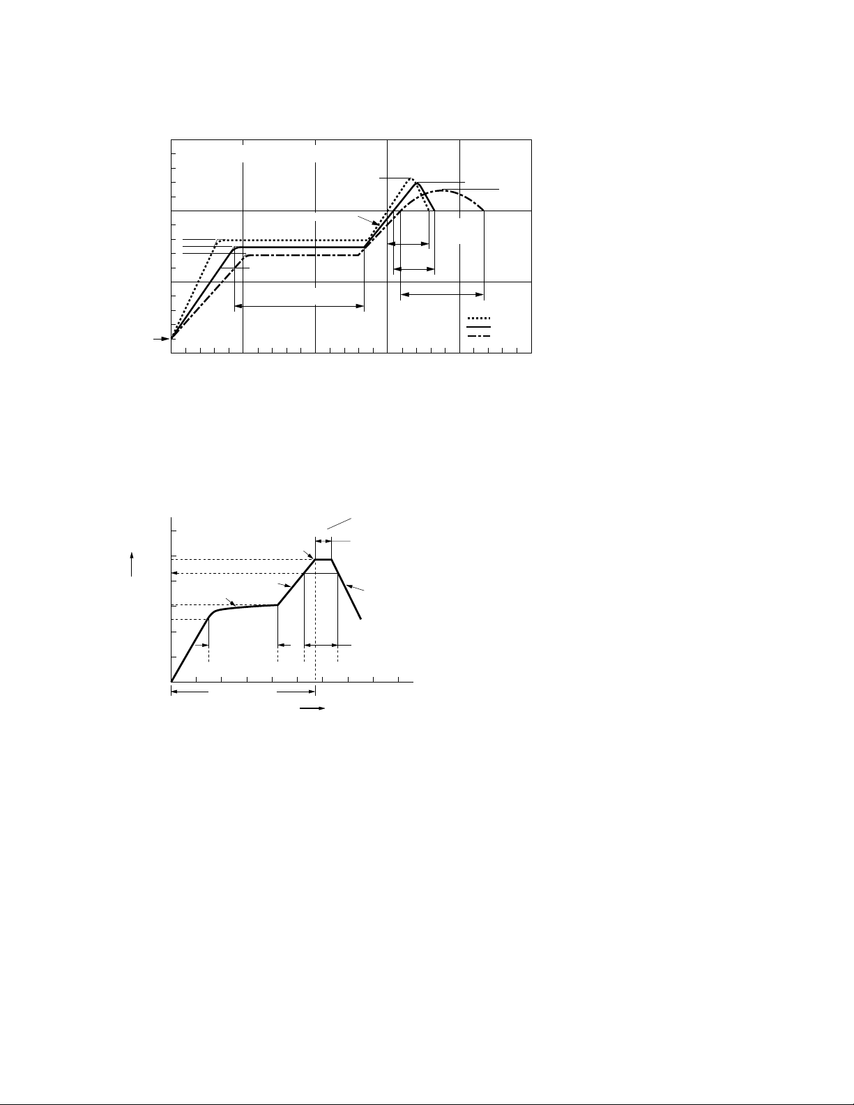
SWITCH AT A: I
5 V
V
O
SWITCH AT B: I
V
O
0.5 V
+3.3 V
R
L
OUTPUT V
MONITORING
NODE
F
F
V
= 0 mA
V
= 7.5 mA
VO (MAX.)
O
CM
(MIN.)
O
I
F
(PEAK)
B
A
V
FF
CM
CM
1
2
3
4
H
L
DUAL CHANNEL
V
GND
V
CM
–
+
PULSE
GENERATOR
Z
= 50 Ω
O
CC
R
L
+3.3 V
OUTPUT V
MONITORING
NODE
O
8
7
0.1 µF
6
BYPASS
5
Figure 9. Test circuit for common mode transient immunity and typical waveforms.
11
Page 12

For product information and a complete list of distributors, please go to our website: www.avagotech.com
Avago, Avago Technologies, and the A logo are trademarks of Avago Technologies Limited in the United States and other countries.
Data subject to change. Copyright © 2006 Avago Technologies Limited. All rights reserved. Obsoletes 5989-3825EN
AV01-0206EN June 14, 2006
 Loading...