

Page 1

ACPL-785J
Lead (Pb) Free
RoHS 6 fully
compliant
RoHS 6 fully compliant options available;
-xxxE denotes a lead-free product
16
15
14
13
12
11
10
9
1
2
3
4
5
6
7
8
FAULT
ABSVAL
V
OUT
V
REF
V
IN+
V
IN-
R
SENSE1
SHORT CIRCUIT FAULT
ISOLATION BOUNDARY
A/D
CONVERTER
MICRO
CONTROLLER
ACPL-785J
16
15
14
13
12
11
10
9
1
2
3
4
5
6
7
8
FAULT
ABSVAL
V
OUT
V
REF
V
IN+
V
IN-
R
SENSE2
ISOLATION BOUNDARY
ACPL-785J
16
15
14
13
12
11
10
9
1
2
3
4
5
6
7
8
FAULT
ABSVAL
V
OUT
V
REF
V
IN+
V
IN-
R
SENSE3
ISOLATION BOUNDARY
ACPL-785J
M
+5 V
OVERLOAD
FAULT
+
–
+
–
3 PHASE ABSOLUTE
VALUE OUTPUT
V
REF
V
TH
3 PHASE
MOTOR
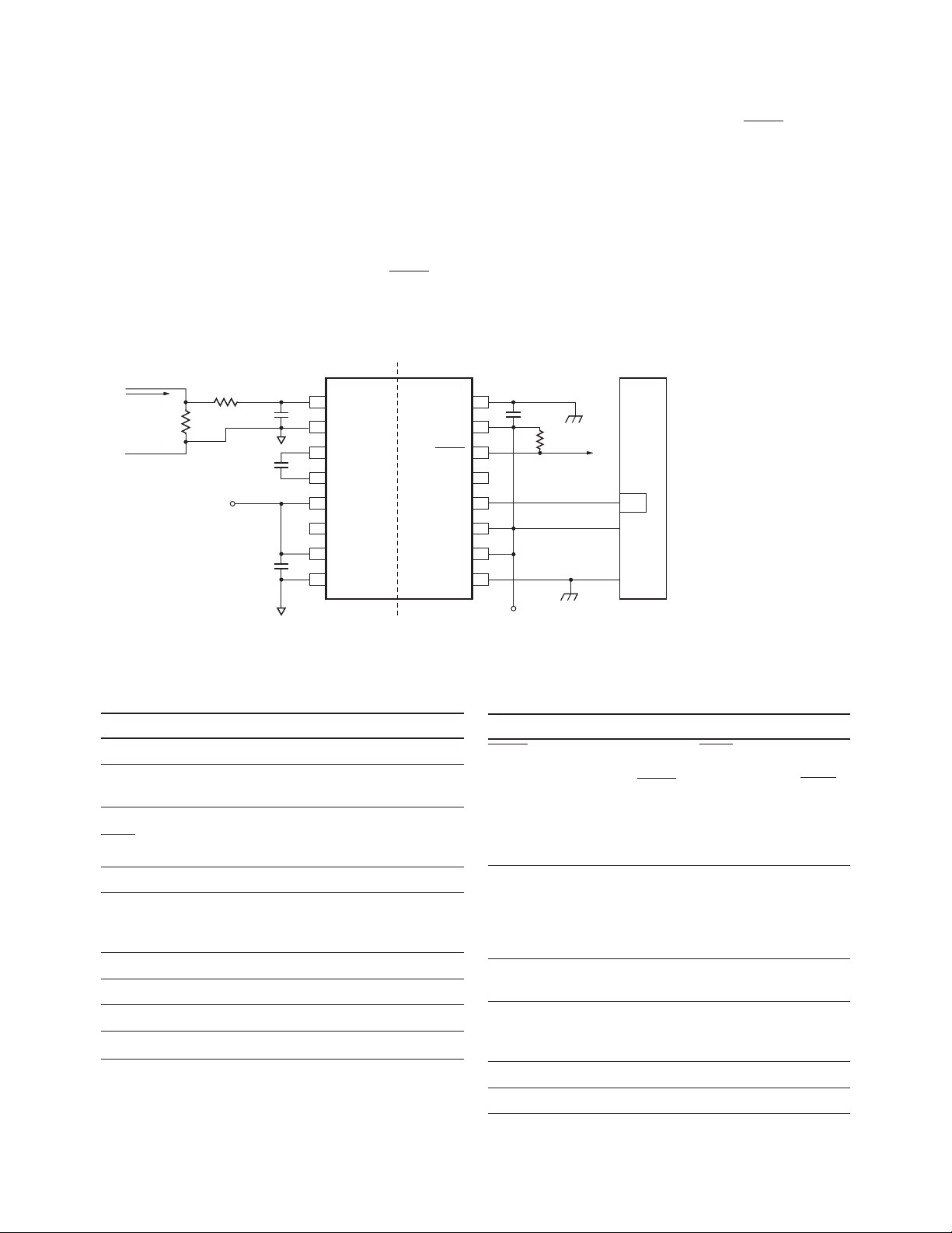
Isolation Amplifier with Short Circuit and Overload Detection
Data Sheet
Description
Avago’s Isolation Amplifier with Short Circuit and
Overload Detection makes motor phase current sensing
compact, affordable and easy-to-implement while satisfying worldwide safety and regulatory requirements.
Applications
• Motor phase and rail current sensing
• Power inverter current and voltage sensing
• Industrial process control
• Data acquisition systems
• General purpose current and voltage sensing
• Traditional current transducer replacements
Features
• Output Voltage Directly Compatible with A/D
Converters (0 V to V
• Fast (3 µs) Short Circuit Detection with Transient Fault
Rejection
• Absolute Value Signal Out put for Overload Detection
• 1 µV/°C Offset Change vs. Temperature
• SO-16 Package
• -40°C to +85°C Operating Temperature Range
• 25 kV/µs Isolation Transient Immunity
• Regulatory Approvals: UL, CSA, IEC/EN/DIN EN
60747-5-5 (891 Vpeak Working Voltage)
Low Cost Three Phase Current Sensing with Short Circuit and Overload Detection
REF
)
CAUTION: It is advised that normal static precautions be taken in handling and assembly of
this component to prevent damage and/or degradation which may be induced by ESD.
Page 2
Description
16
15
14
13
12
11
10
9
1
2
3
4
5
6
7
8
GND
2
V
DD2
FAULT
ABSVAL
V
OUT
V
REF
V
DD2
GND
2
V
IN+
V
IN-
C
H
C
L
V
DD1
V
LED+
V
DD1
GND
1
R
SHUNT
0.02
ISOLATED +5 V
4.7 k
39
.01 F
0.1 F
0.1 F
ISOLATION BOUNDARY
INPUT
CURRENT
+5 V
A/D
V
REF
GND
C
TO OTHER
PHASE
OUTPUTS
+
0.1 F
ACPL-785J
The ACPL-785J isolation amplifier is designed for current
sensing in electronic motor drives. In a typical implementation, motor currents flow through an external resistor
and the resulting analog voltage drop is sensed by the
ACPL-785J. A larger analog output voltage is created
on the other side of the ACPL-785J’s optical isolation
barrier. The output voltage is proportional to the motor
current and can be connected directly to a single-supply
A/D converter. A digital over-range output (FAULT) and
an analog rectified output (ABSVAL) are also provided.
The wire OR-able over-range output (FAULT) is useful
for quick detec tion of short circuit con ditions on any
of the motor phases. The wire-OR-able rectified output
(ABSVAL), simplifies measure-ment of motor load since
it performs polyphase rectification. Since the commonmode voltage swings several hundred volts in tens of
nanoseconds in modern electronic motor drives, the
ACPL-785J was designed to ignore very high commonmode transient slew rates (10 kV/µs).
Figure 1. Current sensing circuit.
Pin Descriptions
Symbol Description
V
Positive input voltage (±200 mV recommended).
IN+
V
Negative input voltage (normally connected to
IN-
GND1).
CH Internal Bias Node. Connections to or between CH
and CL other than the re quired 0.1 µF capacitor
C
L
shown, are not recommended.
V
Supply voltage input (4.5 V to 5.5 V).
DD1
V
LED anode. This pin must be left uncon nected for
LED+
guaranteed data sheet perfor mance. (For optical
coupling testing only.)
V
Supply voltage input (4.5 V to 5.5 V).
DD1
GND1 Ground input.
GND2 Ground input.
V
2
Supply voltage input (4.5 V to 5.5 V).
DD2
Symbol Description
FAULT Short circuit fault output. FAULT changes from a
high to low output voltage within 6 µs after
V
is an open drain output which allows outputs from
all the ACPL-785Js in a circuit to be connected
together (“wired-OR”) forming a single fault signal
for interfacing directly to the micro-controller.
ABSVAL Absolute value of V
when VIN=0 and increases toward V
approaches +256 mV or -256 mV. ABSVAL is
“wired-OR” able and is used for detecting
overloads.
V
Voltage output. Swings from 0 to V
OUT
The nominal gain is V
V
Reference voltage input (4.0 V to V
REF
voltage establishes the full scale output ranges
and gains of V
V
Supply voltage input (4.5 V to 5.5 V).
DD2
GND2 Ground input.
exceeds the FAULT Detection Threshold. FAULT
IN
output. ABSVAL is 0 V
OUT
/504 mV.
REF
and ABSVAL.
OUT
DD2
REF
.
REF
). This
as VIN
Page 3
Ordering Information
9
0.295 ± 0.010
(7.493 ± 0.254)
10111213141516
87654321
0.018
(0.457)
0.138 ± 0.005
(3.505 ± 0.127)
9°
0.406 ± 0.10
(10.312 ± 0.254)
0.408 ± 0.010
(10.160 ± 0.254)
0.025 MIN.
0.008 ± 0.003
(0.203 ± 0.076)
STANDOFF
0.345 ± 0.010
(8.986 ± 0.254)
0–8°
0.018
(0.457)
0.050
(1.270)
ALL LEADS
TO BE
COPLANAR
± 0.002
A 785J
YYWW
TYPE NUMBER
DATE CODE
0.458 (11.63)
0.085 (2.16)
0.025 (0.64)
LAND PATTERN RECOMMENDATION
ACPL-785J is UL Recognized with 3750 Vrms for 1 minute per UL1577.
Part number
ACPL-785J
Option (RoHS
Compliant) Package Surface Mount Tape & Reel
-000E
-060E X X 45 per tube
SO-16
X 45 per tube
IEC/EN/DIN EN
60747-5-5 Quantity
-500E X X 850 per reel
-560E X X X 850 per reel
To order, choose a part number from the part number column and combine with the desired option from the option
column to form an order entry.
Example:
ACPL-785J-560E to order product of 16-Lead Surface Mount package in Tape and Reel packaging with IEC/EN/DIN EN
60747-5-5 Safety Approval and RoHS compliant.
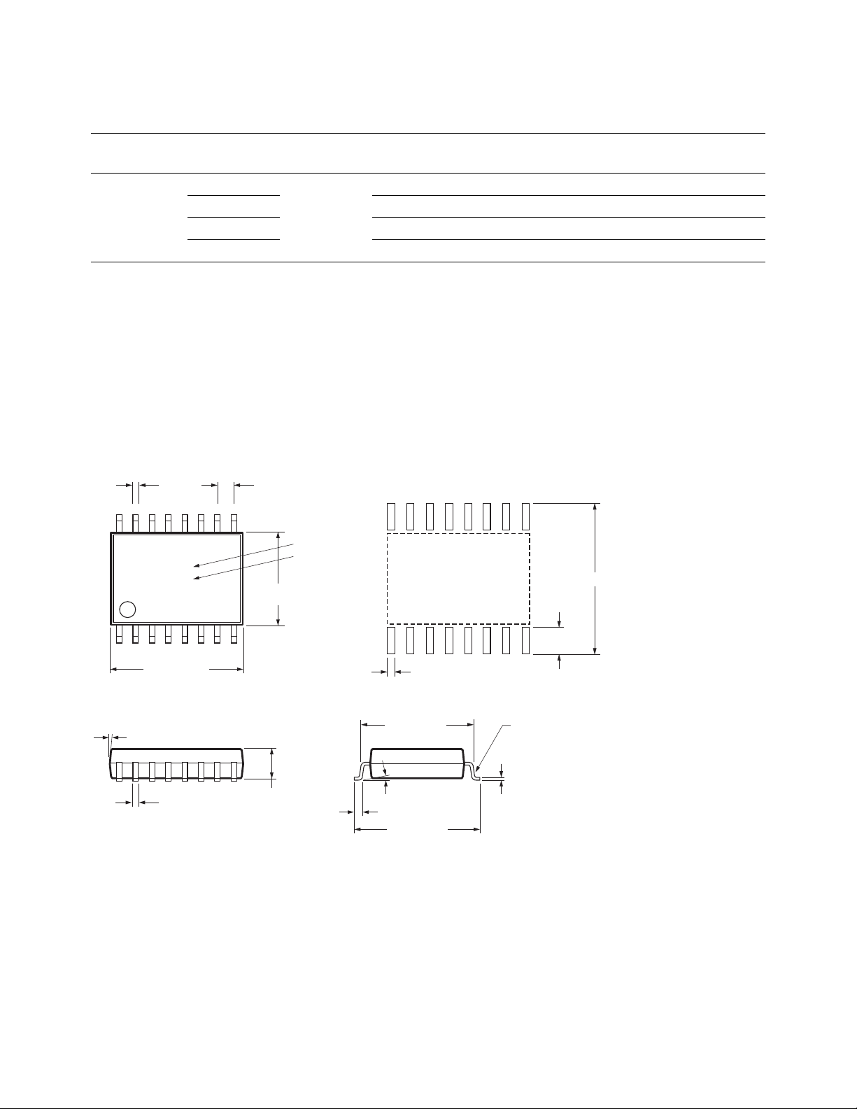
Package Outline Drawings
16-Lead Surface Mount
Dimensions in inches (millimeters)
3
Note: Initial and continued variation in the color of the white mold
compound is normal and does not affect device performance or
reliability.
Note: Floating lead protrusion is 0.25 mm (10 mils) max.
Page 4

Package Characteristics
Parameter Symbol Min. Typ. Max. Units Test Conditions Fig. Notes
Input-Output Momentary
Withstand Voltage
Resistance (Input-Output) R
Capacitance (Input-Output) C
Input IC Junction-to-Case
Thermal Resistance
Output IC Junction-to-Case
Thermal Resistance
V
ISO
I-O
I-O
θjci
θjco
3750 Vrms RH < 50%, t = 1 min.,
TA = 25°C
9
>10
Ω
V
I-O
= 500 V
DC
1.3 pF f = 1 MHz 3
120 °C/W TA = 85°C
100 °C/W TA = 85°C
1,2,3
3
Recommended Pb-Free IR Profile
Recommended reflow condition as per JEDEC Standard,
J-STD-020 (latest revision). Non-Halide Flux should be
used.
Regulatory Information
The ACPL-785J is pending for approvals by the following organizations:
IEC/EN/DIN EN 60747-5-5
Approved with Maximum Working Insulation Voltage
V
IORM
= 891 V
peak
.
UL
Approval under UL 1577, component recognition
program up to V
= 3750 Vrms/1min. File E55361.
ISO
CSA
Approval under CSA Component Acceptance Notice #5,
File CA 88324
4
Page 5

IEC/EN/DIN EN 60747-5-5 Insulation Characteristics*
P
s
– POWER – mW
0
0
TS – CASE TEMPERATURE – °C
20025
800
50 75 100
200
150 175125
400
600
Psi – OUTPUT
Psi – INPUT
Description Symbol Characteristic Unit
Installation classification per DIN VDE 0110/1.89, Table 1
for rated mains voltage ≤ 300 V
for rated mains voltage ≤ 300 V
for rated mains voltage ≤ 600 V
rms
rms
rms
Climatic Classification 55/85/21
Pollution Degree (DIN VDE 0110/1.89) 2
Maximum Working Insulation Voltage V
Input to Output Test Voltage, Method b**
V
x 1.875 = VPR, 100% Production Test with
IORM
tm = 1 sec, Partial discharge < 5 pC
Input to Output Test Voltage, Method a**
V
x 1.6 = VPR, Type and Sample Test, tm = 10 sec,
IORM
Partial discharge < 5 pC
Highest Allowable Overvoltage (Transient Overvoltage t
= 60 sec) V
ini
IORM
V
PR
V
PR
IOTM
Safety-limiting values — maximum values allowed in the
event of a failure, also see Figure 2.
Case Temperature
Input Power
Output Power
Insulation Resistance at T
* Isolation characteristics are guaranteed only within the safety maximum ratings which must be ensured by protective circuits within the
application. Surface Mount Classification is class A in accordance with CECC00802.
** Refer to the optocoupler section of the isolation and Control Components Designer’s Catalog, under Product Safety Regulations section IEC/EN/
DIN EN 6747-5-5, for a detailed description of Method a and Method b partial discharge test profiles.
= 500 V R
SI, VIO
T
S
P
S1, INPUT
P
S1, OUTPUT
S
I-IV
I-III
I-II
891 V
1670 V
1425 V
6000 V
175
400
600
9
>10
PEAK
PEAK
PEAK
PEAK
°C
mW
mW
Ω
Figure 2. Dependence of safety-limiting values on temperature.
5
Page 6

Insulation and Safety Related Specifications
Parameter Symbol Min. Max. Conditions
Minimum External Air Gap
(Clearance)
Minimum External Tracking
(Creepage)
Minimum Internal Plastic Gap 0.5 mm Through insulation distance conductor to conductor,
Tracking Resistance CTI >175 Volts DIN IEC 112/VDE 0303 Part 1
Isolation Group IIIa Material Group (DIN VDE 0110, 1/89, Table 1)
L(101) 8.3 mm Measured from input terminals to output terminals,
shortest distance through air.
L(102) 8.3 mm Measured from input terminals to output terminals,
shortest distance path along body.
usually the straight line distance thickness between the
emitter and detector.
Comparative Tracking Index)
Absolute Maximum Ratings
Parameter Symbol Min. Max. Units Note
Storage Temperature T
Operating Temperature T
Supply Voltages V
Steady-State Input Voltage V
2 Second Transient Input Voltage V
Output Voltage V
S
A
DD1
IN+
IN+
OUT
, V
, V
, V
DD2
IN-
IN-
Absolute Value Output Voltage ABSVAL -0.5 V
Reference Input Voltage V
Reference Input Current I
Output Current I
Absolute Value Current I
FAULT Output Current I
Input IC Power Dissipation P
Output IC Power Dissipation P
REF
REF
VOUT
ABSVAL
FAU LT
I
O
-55 125 °C
-40 100 °C
0.0 5.5 V 4
-2.0 V
-6.0 V
-0.5 V
0 V
+ 0.5 V
DD1
+ 0.5 V
DD1
+ 0.5 V
DD2
+ 0.5 V
DD2
+ 0.5 V V 5
DD2
20 mA
20 mA
20 mA
20 mA
200 mW
200 mW
Recommended Operating Conditions
Parameter Symbol Min. Max. Units Note
Ambient Operating Temperature T
Supply Voltages V
Input Voltage (accurate and linear) V
Input Voltage (functional) V
Reference Input Voltage V
FAULT Output Current I
6
A
DD1
IN+
IN+
REF
FAU LT
, V
, V
, V
DD2
IN-
IN-
-40 85 °C
4.5 5.5 V
-200 200 mV
-2 2 V
4.0 V
DD2
V
4 mA
Page 7

DC Electrical Specifications
Unless otherwise noted, all typicals and figures are at the nominal operating conditions of V
4.0 V, V
DD1
= V
= 5 V and TA = 25°C; all Minimum/Maximum specifications are within the Recommended Operating
DD2
Conditions.
Test
Parameter Symbol Min. Typ. Max. Units
Input Offset
Voltage
Magnitude of Input
Offset Change vs.
Temperature
V
Gain G V
OUT
Magnitude of V
Gain Change vs.
OUT
Temperature
V
200 mV
OUT
Nonlinearity
Maximum Input
Voltage Before
V
Clipping
OUT
FAULT Detection
Threshold
FAULT Low
Output Voltage
FAULT High
Output Current
ABSVAL Output
Error
Input Supply
Current
Output Supply
Current
Reference Voltage
Input Current
Input Current I
Input Resistance R
V
Output
OUT
Resistance
ABSVAL Output
Resistance
Input DC CommonMode Rejection
Ratio
V
OS
|∆VOS/∆TA|
|∆G/∆TA|
NL
200
|V
IN+|MAX
|V
| 230 256 280 mV 10 9
THF
V
OLF
I
OHF
e
ABS
-3 0 3 mV V
/504
REF
mV - 5%
1 10
V
/504 mVV
REF
/504
REF
mV + 5%
µV/°C
V/V |V
50 300 ppm/°C |V
0.06 0.4 % |V
256 mV
350 800 mV IOL = 4 mA
0.2 15
µA
0.6 2 % of
full scale
output
I
DD1
I
DD2
I
VREF
IN+
IN
R
OUT
R
ABS
CMRR
IN
10.7 20 mA
10.4 20 mA
0.26 1 mA
-350 nA V
800
0.2
0.3
kΩ
Ω
Ω
85 dB 11
Conditions Fig. Note
= 0 V,
IN+
TA = –40°C to +85°C
V
= 0 V,
IN+
TA = –40°C to +85°C
| < 200 mV,
IN+
TA = 25°C
| < 200 mV,
IN+
TA = 25°C
| < 200 mV,
IN+
TA = –40°C to +85°C
V
= V
FAU LT
DD2
= 0 V
IN+
V
= 0 V
IN+
= 0, V
IN+
= 0 V, V
IN-
3, 4,
6
5
7
6,7,
8,9
6,7,
8,9
6,7,
8,9
11 10
=
REF
8
7
Page 8

AC Electrical Specifications
Unless otherwise noted, all typicals and figures are at the nominal operating conditions of V
4.0 V, V
DD1
= V
= 5 V and TA = 25°C; all Minimum/Maximum specifications are within the Recommended Operating
DD2
= 0, V
IN+
= 0 V, V
IN-
Conditions.
Parameter Symbol Min. Typ. Max. Units Test Conditions Fig. Note
V
Bandwidth (-3dB) BW 20 30 kHz V
OUT
V
Noise N
OUT
VIN to V
(50 - 50%)
V
OUT
(10–90)
Signal Delay
OUT
Rise/Fall Time
ABSVAL Signal Delay t
ABSVAL Rise/Fall Time
(10–90%)
FAULT Detection Delay t
FAULT Release Delay t
Transient Fault Rejection t
Common Mode Transient
OUT
t
DSIG
t
RFSIG
DABS
t
RFABS
FHL
FLH
REJECT
10 20
1 2
CMTI 10 25
2.2 4 mVrms V
9 20
10 25
9 20
10 25
3 6
µs
µs
µs
µs
µs
µs
µs
kV/µs
Immunity
Common-Mode Rejection
CMRR >140 dB 18
Ratio at 60 Hz
= 200 mV
IN+
sine wave.
= 0 V 20 12
IN+
V
= 50 mV to
IN+
200 mV step.
V
= 50 mV to
IN+
200 mV step.
V
= 50 mV to
IN+
200 mV step.
V
= 50 mV to
IN+
200 mV step.
V
= 0 mV to
IN+
±500 mV step.
V
= ±500 mV to
IN+
0 mV step.
V
= 0 mV to
IN+
±500 mV pulse.
For V
OUT
ABSVAL outputs.
pk-pk
, FAULT, and
12,
20
14,
20
14,
20
14,
20
14,
20
15,
20
16,
20
17,
20
13
14
15
16
17
REF
=
8
Page 9

Notes:
1. In accordance with UL1577, each optocoupler is proof tested by applying an insulation test voltage ≥ 4500 Vrms for 1 second (leakage detection
current limit, I
60747-5-5 Insulation Characteristic Table, if applicable.
≤ 5 µA). This test is performed before the 100% production test for partial discharge (method b) shown in IEC/EN/DIN EN
I-O
2. The Input-Output Momentary Withstand Voltage is a dielectric voltage rating that should not be interpreted as an input-output
continuous voltage rating. For the continuous voltage rating refer to your equipment level safety specification or IEC/EN/DIN EN 60747-5-5
insulation characteristics table.
3. Device considered a two terminal device: pins 1-8 shorted together and pins 9-16 shorted together.
4. V
must be applied to both pins 5 and 7. V
DD1
5. If V
exceeds V
REF
6. Input Offset voltage is defined as the DC Input voltage required to obtain an output voltage (at pin 12) of V
(due to power-up sequence, for example), the current into pin 11 (I
DD2
7. This is the Absolute Value of Input Offset Change vs. Temperature.
8. This is the Absolute Value of V
9. |V
| must exceed this amount in order for the FAULT output to be activated.
IN+
10. ABSVAL is derived from V
VIN approaches +256 mV or -256 mV. ε
V
. ε
is expressed in terms of percent of full scale and is defined as:
OUT
ABS
|ABSVAL - 2 x | V
V
REF
Gain Change vs. Temperature.
OUT
(which has the gain and offset tolerances stated earlier). ABSVAL is 0 V when VIN = 0 V and increases toward V
OUT
- V
/ 2| |
OUT
REF
x 100.
must be applied to both pins 10 and 15.
DD2
is the difference between the actual ABSVAL output and what ABSVAL should be, given the value of
ABS
) should be limited to 20 mA or less.
REF
/2.
REF
as
REF
11. CMRRIN is defined as the ratio of the gain for differential inputs applied between pins 1 and 2 to the gain for common mode inputs applied to
both pins 1 and 2 with respect to pin 8.
12. The signal-to-noise ratio of the ACPL-785J can be improved with the addition of an external low pass filter to the output. See Frequently Asked
Question #4.2 in the Applications Information Section at the end of this data sheet.
13. As measured from 50% of VIN to 50% of V
14. This is the amount of time from when the FAULT Detection Threshold (230 mV ≤ V
low.
15. This is the amount of time for the FAULT Output to return to a high state once the FAULT Detection Threshold (230 mV ≤ V
longer exceeded.
16. Input pulses shorter than the fault rejection pulse width (t
in the Applications Information Section at the end of this data sheet for additional detail on how to avoid false tripping of the FAULT output due
OUT
.
≤ 280 mV) is exceeded to when the FAULT output goes
THF
≤ 280 mV) is no
THF
), will not activate the FAULT (pin 14) output. See Frequently Asked Question #2.3
REJECT
to cable capacitance charging transients.
17. CMTI is also known as Common Mode Rejection or Isolation Mode Rejection. It is tested by applying an exponentially rising falling voltage
step on pin 8 (GND1) with respect to pin 9 (GND2). The rise time of the test waveform is set to approximately 50 ns. The amplitude of the step
is adjusted until V
continue to function if more than 10 kV/µs common mode slopes are applied, as long as the break-down voltage limitations are observed. [The
(pin 12) exhibits more than 100 mV deviation from the average output voltage for more than 1µs. The ACPL-785J will
OUT
ACPL-785J still functions with common mode slopes above 10 kV/µs, but output noise may increase to as much as 600 mV peak to peak.]
18. CMRR is defined as the ratio of differential signal gain (signal applied differentially between pins 1 and 2) to the common mode gain (input pins
tied to pin 8 and the signal applied between the input and the output of the isolation amplifier) at 60 Hz, expressed in dB.
9
Page 10

INPUT OFFSET CHANGE - DVOS - uV
-40
-800.0
TEMPERATURE – DEG C
-20
800.0
0 20
-400.0
60 80
TYPICAL
MAX
40
0
400.0
600.0
200.0
-200.0
-600.0
V
OS
OFFSET CHANGE – V
4.5
-800
INPUT SUPPLY VOLTAGE – V
DD1
– V
800
4.75 5.0 5.25 5.5
0
600
400
200
-200
-400
-600
V
OS
OFFSET CHANGE – V
4.5
-800
OUTPUT SUPPLY VOLTAGE – V
DD2
– V
800
4.75 5.0 5.25 5.5
0
600
400
200
-200
-400
-600
V
OUT
– OUTPUT VOLTAGE – V
-300
0
INPUT VOLTAGE – VIN – mV
4.0
-200 0 100 300
2.0
3.5
3.0
2.5
1.5
1.0
0.5
-100 200
GAIN CHANGE-%
-40
-2.0
TEMPERATURE – °C
-20
2.0
0 20
-1.0
60 80
TYPICAL
WORST CASE
40
0
1.0
1.5
0.5
-0.5
-1.5
GAIN CHANGE-%
4.5
-2.0
INPUT SUPPLY VOLTAGE – V
DD1
– V
2.0
4.75 5.0 5.25 5.5
0
1.5
1.0
0.5
-0.5
-1.0
-1.5
Figure 3. Input offset voltage change vs. temperature. Figure 4. Input offset voltage change vs. V
.
DD1
Figure 5. Input offset voltage change vs. V
. Figure 6. V
DD2
vs. VIN.
OUT
Figure 7. Gain change vs. temperature. Figure 8. Gain change vs. V
10
.
DD1
Page 11

GAIN CHANGE-%
4.5
-2.0
OUTPUT SUPPLY VOLTAGE – V
DD2
– V
2.0
4.75 5.0 5.25 5.5
0
1.5
1.0
0.5
-0.5
-1.0
-1.5
FAULT OUTPUT VOLTAGE – FAULTBAR – V
-300
0
INPUT VOLTAGE – VIN – mV
5.0
-200 0 100 300
2.0
3.5
3.0
2.5
1.5
1.0
0.5
-100 200
4.0
4.5
BANDWIDTH – kHz
-40
25
TEMPERATURE – °C
-20
35
0 20 60 8040
30
34
33
32
31
29
28
27
26
ABSVAL – ABSOLUTE VALUE OUTPUT – V
-300
0
INPUT VOLTAGE – VIN – mV
4.0
-200 0 100 300
2.0
3.5
3.0
2.5
1.5
1.0
0.5
-100 200
FAULT DETECTION DELAY – s
-40
2.5
TEMPERATURE – °C
-20
3.5
0 20 60 80
40
3.0
2.75
3.25
5.00 s/DIV
0 V
2.5 V
5 V
0 V
2.5 V
5 V
0 V
2.5 V
5 V
-300 mV
0 mV
300 mV
FAULT (PIN 14) 2.5 V/D
VIN 300 mV/D
V
OUT
(PIN 12) 2.5 V/D
ABSVAL (PIN 13)
2.5 V/D
Figure 9. Gain change vs. V
. Figure 10. FAULT output voltage vs. VIN.
DD2
Figure 11. ABSVAL output voltage vs. VIN. Figure 12. Bandwidth vs. temperature.
Figure 13. FAULT detection delay vs. temperature. Figure 14. Step response, 0 to 200 mV input, at V
11
REF
= 5 V.
Page 12

0 V
2.5 V
5 V
0 V
2.5 V
5 V
0 V
2.5 V
5 V
-300 mV
0 mV
300 mV
5.00 s/DIV
V
IN
300 mV/D
V
OUT
(PIN 12)
2.5 V/D
FAULT (PIN 14) 2.5 V/D
ABSVAL (PIN 13)
2.5 V/D
0 V
2.5 V
5 V
0 V
2.5 V
5 V
0 V
2.5 V
5 V
-300 mV
0 mV
300 mV
5.00 s/DIV
VIN 300 mV/D
V
OUT
(PIN 12) 2.5 V/D
ABSVAL (PIN 13)
2.5 V/D
FAULT (PIN 14)
2.5 V/D
0 V
2.5 V
5.0 V
0 V
2.5 V
5.0 V
0 V
2.5 V
5.0 V
-2 V
0 mV
2 V
5.00 s/DIV
V
IN
2.0 V/D
V
OUT
(PIN 12) 2.5 V/D
ABSVAL (PIN 13)
2.5 V/D
FAULT (PIN 14)
2.5 V/D
0 V
2.5 V
5 V
0 V
2.5 V
5 V
0 V
2.5 V
5 V
-300 mV
0 mV
300 mV
5.00 s/DIV
VIN 300 mV/D
V
OUT
(PIN 12) 2.5 V/D
ABSVAL (PIN 13) 2.5 V/D
FAULT (PIN 14) 2.5 V/D
0 V
2.5 V
5 V
0 V
2.5 V
5 V
0 V
2.5 V
5 V
-300 mV
0 mV
300 mV
100 s/DIV
VIN 300 mV/D
V
OUT
(PIN 12) 2.5 V/D
ABSVAL (PIN 13) 2.5 V/D
FAULT (PIN 14) 2.5 V/D
Figure 15. FAULT detection, 0 to 300 mV input, at V
= 5 V. Figure 16. FAULT release, 300 to 0 mV input, at V
REF
REF
= 5 V.
Figure 17. FAULT rejecting a 1 µs, 0 to 2 V to 0 input. Rejection is
independent of amplitude.
Figure 19. Sine response 400 mV pk to pk 4 kHz input, at V
12
REF
= 5 V.
Figure 18. Detection of 6 µs fault 0 to 2 V to 0 input, at V
REF
= 5 V.
Page 13

Figure 20. AC test circuit.
14
13
12
11
10,15
9, 16
1
3
4
6
5, 7
2, 8
FAULT
ABSVAL
V
OUT
V
DD2
V
IN+
V
DD1
4.7 k
50
0.01 F
0.1 F
0.1 F
ACPL-785J
V
REF
10
0.1 F
0.1 F
5 V
1
V
REF
V
OUT
FAULT
ABSVAL
V
DD2
V
DD2
GND
2
GND
2
V
IN+
V
IN-
C
H
C
L
V
LED+
V
DD1
V
DD1
GND
1
2
3
4
6
5
7
8
11
12
13
14
15
10
9
16
MODULATOR
256 mV
REFERENCE
FAULT
DETECT
ENCODER
RECTIFIER
DECODER D/A LPF
ACPL-785J
Figure 21. Internal block diagram.
13
Page 14

ABSVAL – V
0
0
TIME – SECONDS
4.0
0.01 0.02 0.03 0.04
2.0
3.0
1.0
ABSVAL – V
0
0
TIME – SECONDS
4.0
0.01 0.02 0.03 0.04
2.0
3.0
1.0
ABSVAL – V
0
0
TIME – SECONDS
4.0
0.01 0.02 0.03 0.04
2.0
3.0
1.0
Applications Information
Production Description
Figure 21 shows the internal block diagram of the
ACPL-785J. The analog input (VIN) is con verted to a
digital signal using a sigma-delta (∑-∆) analog to
digital (A/D) converter. This A/D samples the input 6
million times per second and generates a high speed
1-bit output representing the input very accurately.
This 1 bit data stream is transmitted via a light emitting
diode (LED) over the optical barrier after encoding.
The detector converts the optical signal back to a bit
stream. This bit stream is decoded and drives a 1 bit
digital to analog (D/A) con verter. Finally a low pass filter
and output buffer drive the output signal (V
) which
OUT
linearly rep re sents the analog input. The output signal
full-scale range is determined by the external reference
voltage (V
). By sharing this reference voltage (which
REF
can be the supply voltage), the full-scale range of the
ACPL-785J can precisely match the full-scale range of
an external A/D converter.
In addition, the ACPL-785J compares the analog input
(VIN) to both the negative and positive full-scale values.
If the input exceeds the full-scale range, the short-circuit
fault output (FAULT) is activated quickly. This feature
operates indepen dently of the ∑-∆ A/D converter in
order to provide the high-speed response (typically 3 µs)
needed to protect power tran sistors. The FAULT output
is wire OR-able so that a short circuit on any one motor
phase can be detected using only one signal.
One other output is provided — the rectified output
(ABSVAL). This output is also wire OR-able. The motor
phase having the highest instantaneous rectified output
pulls the common output high. When three sinusoidal motor phases are combined, the rectified output
(ABSVAL) is essentially a DC signal represent ing the rms
motor current. This single DC signal and a threshold comparator can indicate motor overload conditions before
dam age to the motor or drive occur. Figure 22 shows the
ABSVAL output when 3 ACPL-785Js are used to monitor
a sinusoidal 60 Hz current. Figures 23 and 24 show the
ABSVAL output when only 2 or 1 of the 3 phases are
monitored, respectively.
The ACPL-785J’s other main function is to provide
galvanic isolation between the analog input and the
analog output. An internal voltage reference determines the full-scale analog input range of the modulator
(approximately ±256 mV); an input range of ±200 mV is
recommended to achieve optimal performance.
Figure 24. ABSVAL with 1 phase.
14
Figure 23. ABSVAL with 2 phases, wired-ORed together.Figure 22. ABSVAL with 3 phases, wired-ORed together.
Page 15

Figure 25. Recommended applications circuit.
16
15
14
13
12
11
10
9
5
1
2
8
7
3
4
6
GND
2
V
DD2
FAULT
ABSVAL
V
OUT
V
REF
V
DD2
GND
2
V
DD1
V
IN+
V
IN-
GND
1
V
DD1
C
H
C
L
V
LED+
R2
39
+
R4
C1
0.1 F
C2
0.01 F
FLOATING
POWER
SUPPLY
HV+
+
–
+
R1
R
SENSE
HV-
MOTOR
D1
5.1 V
GATE DRIVE
CIRCUIT
ACPL-785J
16
15
14
13
12
11
10
9
1
2
3
4
5
6
7
8
GND
2
V
DD2
FAULT
ABSVAL
V
OUT
V
REF
V
DD2
GND
2
V
IN+
V
IN-
C
H
C
L
V
DD1
V
LED1+
V
DD1
GND
1
R
SHUNT
0.02
ISOLATED +5 V
R3 4.7 k
R2
39
.01 F
C3
0.1 F
C1
0.1 F
ACPL-785J
INPUT
CURRENT
+5 V
A/D
V
REF
GND
C
TO OTHER
PHASE OUTPUTS
+
R1
C2
C6
0.1 F
C4C8 C7 C5
C5 = C7 = C8 = 470 pF
C4 = 0.1 F
Figure 26. Recommended supply and sense resistor connections.
15
Page 16

Analog Interfacing
Power Supplies and Bypassing
The recommended supply con nec tions are shown in
Figure 26. A floating power supply (which in many
applications could be the same supply that is used to
drive the high-side power transistor) is regulated to 5 V
using a simple zener diode (D1); the value of resistor R4
should be chosen to supply sufficient current from the
existing floating supply. The voltage from the current
sensing resistor (Rsense) is applied to the input of the
ACPL-785J through an RC anti-aliasing filter (R2 and C2).
Although the application cir cuit is relatively simple, a few
re c ommendations should be followed to ensure optimal
performance.
The power supply for the ACPL-785J is most often
obtained from the same supply used to power the
power transistor gate drive circuit. If a dedicated supply
is required, in many cases it is possible to add an additional winding on an existing trans former. Otherwise,
some sort of simple isolated supply can be used, such as
a line powered transformer or a high-frequency DC-DC
converter.
An inexpensive 78L05 three-terminal regulator can also
be used to reduce the floating supply voltage to 5 V. To
help attenuate high-frequency power supply noise or
ripple, a resistor or inductor can be used in series with
the input of the regulator to form a low-pass filter with
the regulator’s input bypass capacitor.
As shown in Figure 25, 0.1 µF bypass capacitors (C1,
C3, C4, and C6) should be located as close as possible
to the pins of the ACPL-785J. The bypass capacitors are
required because of the high-speed digital nature of the
signals inside the ACPL-785J. A 0.01 µF bypass capacitor
(C2) is also recommended at the input due to the
switched-capacitor nature of the input circuit. The input
bypass capacitor also forms part of the anti-aliasing filter,
which is recommended to prevent high-frequency noise
from aliasing down to lower frequencies and interfering with the input signal. The input filter also performs
an important reliability function — it reduces transient
spikes from ESD events flowing through the current
sensing resistor.
PC Board Layout
The design of the printed circuit board (PCB) should
follow good layout practices, such as keeping bypass
capacitors close to the supply pins, keeping output
signals away from input signals, the use of ground and
power planes, etc. In addition, the layout of the PCB
can also affect the isolation transient immunity (CMTI)
of the ACPL-785J, due primarily to stray capacitive
coupling between the input and the output circuits. To
obtain optimal CMTI performance, the layout of the PC
board should minimize any stray coupling by maintaining the maximum possible distance between the input
and output sides of the circuit and ensuring that any
ground or power plane on the PC board does not pass
directly below or extend much wider than the body of
the ACPL-785J.
TOP LAYER
Figure 27. Example printed circuit board layout.
16
BOTTOM LAYER
Page 17

Current Sensing Resistors
MOTOR OUTPUT POWER – HORSEPOWER
0
0
MOTOR PHASE CURRENT – A (rms)
40
5 20 25 35
20
35
30
25
15
10
5
10 15 30
440
380
220
120
The current sensing resistor should have low resistance (to minimize power dissipation), low inductance
(to minimize di/dt induced voltage spikes which could
adversely affect operation), and reasonable tolerance (to
main tain overall circuit accuracy). Choosing a particular
value for the resistor is usually a compro mise between
minimizing power dissipation and maximizing ac curacy.
Smaller sense resistance decreases power dissipation,
while larger sense resistance can improve circuit accuracy
by utilizing the full input range of the ACPL-785J.
The first step in selecting a sense resistor is determining
how much current the resistor will be sens ing. The graph
in Figure 28 shows the rms current in each phase of a
three-phase induction motor as a function of average
motor output power (in horse power, hp) and motor
drive supply voltage. The maximum value of the sense
resistor is determined by the current being measured
and the maximum recommended input voltage of the
isolation amplifier. The maxi mum sense resistance can
be calculated by taking the maxi mum recommended
input voltage and dividing by the peak current that the
sense resistor should see during normal operation. For
example, if a motor will have a maximum rms current
of 10 A and can experience up to 50% overloads during
normal operation, then the peak current is 21.1 A (=10 x
1.414 x 1.5). Assuming a maximum input voltage of 200
mV, the maximum value of sense resistance in this case
would be about 10 mΩ.
The maximum average power dissipation in the sense
resistor can also be easily calculated by multiplying the
sense resistance times the square of the maximum rms
current, which is about 1 W in the previous example.
If the power dissipation in the sense resistor is too high,
the resistance can be decreased below the maximum
value to decrease power dissipation. The minimum
value of the sense resistor is limited by precision and
accuracy requirements of the design. As the resistance
value is reduced, the output voltage across the resistor
is also reduced, which means that the offset and noise,
which are fixed, become a larger percentage of the signal
amplitude. The selected value of the sense resistor will
fall somewhere between the minimum and maximum
values, depending on the particular requirements of a
specific design.
When sensing currents large enough to cause significant
heating of the sense resistor, the temperature coefficient
(tempco) of the resistor can introduce nonlinearity due
to the signal dependent temperature rise of the resistor.
The effect increases as the resistor-to-ambient thermal
resistance increases. This effect can be minimized by
reducing the thermal resistance of the current sensing
resistor or by using a resistor with a lower tempco.
Lowering the thermal resistance can be accomplished
by reposi tion ing the current sensing resistor on the PC
board, by using larger PC board traces to carry away
more heat, or by using a heat sink.
For a two-terminal current sensing resistor, as the value
of resistance decreases, the resistance of the leads
become a significant per centage of the total resistance.
This has two primary effects on resistor accuracy. First,
the effective resistance of the sense resistor can become
dependent on factors such as how long the leads are, how
they are bent, how far they are inserted into the board,
and how far solder wicks up the leads during assembly
(these issues will be discussed in more detail shortly).
Second, the leads are typically made from a material,
such as copper, which has a much higher tempco than
the material from which the resis tive element itself is
made, result ing in a higher tempco overall.
Figure 28. Motor output horsepower vs. motor phase current and supply
voltage.
17
Both of these effects are eliminated when a four-terminal
current sensing resistor is used. A four-terminal resistor
has two additional terminals that are Kelvin-connected
directly across the resistive element itself; these two
terminals are used to monitor the voltage across the
resistive element while the other two terminals are used
to carry the load current. Because of the Kelvin connection, any voltage drops across the leads carrying the load
current should have no impact on the measured voltage.
Page 18

When laying out a PC board for the current sensing
resistors, a couple of points should be kept in mind.
The Kelvin connections to the resistor should be
brought together under the body of the resistor and
then run very close to each other to the input of the
ACPL-785J; this minimizes the loop area of the connection and reduces the possibility of stray magnetic
fields from interfering with the measured signal. If
the sense resistor is not located on the same PC board as
the ACPL-785J circuit, a tightly twisted pair of wires can
accomplish the same thing.
Also, multiple layers of the PC board can be used to
increase current carrying capacity. Numerous platedthrough vias should surround each non-Kelvin terminal of
the sense resistor to help distribute the current between
the layers of the PC board. The PC board should use 2 or
4 oz. copper for the layers, resulting in a current carrying
capacity in excess of 20 A. Making the current carrying
traces on the PC board fairly large can also improve the
sense resistor’s power dissipation capability by acting
as a heat sink. Liberal use of vias where the load current
enters and exits the PC board is also recommended.
Sense Resistor Connections
The recommended method for connecting the ACPL-785J
to the current sensing resistor is shown in Figure 26. V
(pin 1 of the ACPL-785J) is connected to the positive
terminal of the sense resistor, while V
(pin 2) is shorted
IN-
to GND1 (pin 8), with the power-supply return path functioning as the sense line to the negative terminal of the
current sense resistor. This allows a single pair of wires
or PC board traces to connect the ACPL-785J circuit to
the sense resistor. By referencing the input circuit to
the negative side of the sense resistor, any load current
induced noise transients on the resistor are seen as a
common-mode signal and will not interfere with the
current-sense signal. This is important because the large
load currents flowing through the motor drive, along
with the parasitic inductances inherent in the wiring of
the circuit, can generate both noise spikes and offsets
that are rela tively large compared to the small voltages
that are being measured across the current sensing
resistor.
If the same power supply is used both for the gate drive circuit
and for the current sensing circuit, it is very important
that the connection from GND1 of the ACPL-785J to the
sense resistor be the only return path for supply current
to the gate drive power supply in order to eliminate
potential ground loop problems. The only direct connection between the ACPL-785J circuit and the gate drive
circuit should be the positive power supply line. Please
refer to Avago Technologies’ Applications Note 1078 for
additional information on using Isolation Amplifiers.
IN+
18
Page 19

Frequently Asked Questions about the ACPL-785J
1. The Basics
1.1: Why should I use the ACPL-785J for
sensing current when Hall-effect
sensors are available which don’t
need an isolated supply voltage?
1.2: What is the purpose of the V
input?
1.3: What is the purpose of the rectified
(ABSVAL) output on pin 13?
2. Sense Resistor and Input Filter
2.1: Where do I get 10 mΩ resistors? I
have never seen one that low.
2.2: Should I connect both inputs
across the sense resistor instead of
grounding V
2.3: How can I avoid false tripping of the
fault output due to cable capacitance
charging transients?
directly to pin 8?
IN-
Historically, motor control current sense designs have required trade-offs between
signal accuracy, response time, and the use of discrete components to detect short
circuit and overload conditions. The ACPL-785J greatly simplifies current-sense designs
by providing an output voltage which can connect directly to an A/D converter as well
as integrated short circuit and overload detection (eliminating the need for external
circuitry). Available in an auto-insertable, SO-16 package, the ACPL-785J is smaller
than and has better linearity, offset vs. temperature and Common Mode Rejection
(CMR) performance than most Hall-effect sensors.
The V
REF
input establishes the full scale output range. V
REF
supply voltage (V
ACPL-785J is the output full scale range divided by 504 mV.
When 3 phases are wire-ORed together, the 3 phase AC currents are combined to
form a DC voltage with very little ripple on it. This can be simply filtered and used
to monitor the motor load. Moderate overload currents which don’t trip the FAULT
output can thus be detected easily.
Although less common than values above 10 Ω, there are quite a few manufacturers of resistors suitable for measuring currents up to 50 A when combined with the
ACPL-785J. Example product information may be found at Vishay’s web site (http://
www.vishay.com) and Isotek’s web site (http://www.isotekcorp.com).
This is not necessary, but it will work. If you do, be sure to use an RC filter on both pin
1 (V
) and pin 2 (V
IN+
In PWM motor drives there are brief spikes of current flowing in the wires leading to
the motor each time a phase voltage is switched between states. The amplitude and
duration of these current spikes is determined by the slew rate of the power transistors and the wiring impedances. To avoid false tripping of the FAULT output (pin 14)
the ACPL-785J includes a blanking filter. This filter ignores over-range input conditions
shorter than 1 µs. For very long motor wires, it may be necessary to increase the time
constant of the input RC antialiasing filter to keep the peak value of the ACPL-785J
inputs below ±230 mV. For example, a 39 Ω, 0.047 µF RC filter on pin 1 will ensure that
2 µs wide 500 mV pulses across the sense resistor do not trip the FAULT output.
) or a voltage between 4 V and V
DD2
) to limit the input voltage at both pads.
IN-
can be connected to the
REF
. The nominal gain of the
DD2
2.4: Do I really need an RC filter on the
input? What is it for? Are other values
of R and C okay?
2.5: How do I ensure that the ACPL-785J
is not destroyed as a result of short
circuit conditions which cause
voltage drops across the sense
resistor that exceed the ratings of
the ACPL-785J’s inputs?
19
This filter prevents damage from input spikes which may go beyond the absolute
maximum ratings of the ACPL-785J inputs during ESD and other transient events. The
filter also prevents aliasing of high frequency (above 3 MHz) noise at the sampled
input. Other RC values are certainly OK, but should be chosen to prevent the input
voltage (pin 1) from exceeding ±5 V for any conceivable current waveform in the sense
resistor. Remember to account for inductance of the sense resistor since it is possible
to momentarily have tens of volts across even a 1 mΩ resistor if di/dt is quite large.
Select the sense resistor so that it will have less than 5 V drop when short circuits
occur. The only other requirement is to shut down the drive before the sense resistor is
damaged or its solder joints melt. This ensures that the input of the ACPL-785J cannot
be damaged by sense resistors going open-circuit.
Page 20

3. Isolation and Insulation
3.1: How many volts will the ACPL-785J
withstand?
3.2: What happens if I don’t use the
470 pF output capacitors Avago
recommends?
4. Accuracy
4.1: What is the meaning of the offset
errors and gain errors in terms of the
output?
4.2: Can the signal to noise ratio be
improved?
The momentary (1 minute) withstand voltage is 3750 V rms per UL1577 and CSA
Component Acceptance Notice #5.
These capacitors are to reduce the narrow output spikes caused by high common
mode slew rates. If your application does not have rapid common mode voltage
changes, these capacitors are not needed.
For zero input, the output should ideally be 1/2 of V
output relationship is V
voltage needed to make the output equal to 1/2 of V
divided by 0.504 V. Offset errors change only the DC input
REF
slope of the input/output relationship. For example, if V
7.937 V/V. For zero input, the output should be 2.000 V. Input offset voltage of ±3 mV
. The nominal slope of the input/
REF
. Gain errors change only the
REF
is 4.0 V, the gain should be
REF
means the output voltage will be 2.000 V ±0.003*7.937 or 2.000 ±23.8 mV when the
input is zero. Gain tolerance of ±5% means that the slope will be 7.937 ±0.397. Over
the full range of ±3 mV input offset error and ±5% gain error, the output voltage will
be 2.000 ±25.0 mV when the input is zero.
Yes. Some noise energy exists beyond the 30 kHz bandwidth of the ACPL-785J.
An external RC low pass filter can be used to improve the signal to noise ratio. For
example, a 680 Ω, 4700 pF RC filter will cut the rms output noise roughly by a factor
of 2. This filter reduces the -3dB signal bandwidth only by about 10%. In applications
needing only a few kHz bandwidth even better noise performance can be obtained.
The noise spectral density is roughly 400 nV/√ Hz below 15 kHz (input referred). As an
example, a 2 kHz (680 Ω, 0.1 µF) RC low pass filter reduces output noise to a typical
value of 0.08 mVrms.
4.3: I need 1% tolerance on gain. Does
Avago sell a more precise version?
4.4: The output doesn’t go all the way
to V
when the input is above full
REF
scale. Why not?
4.5: Does the gain change if the internal
LED light output degrades with
time?
4.6: Why is gain defined as V
not V
/512 mV as expected, based
REF
/504 mV,
REF
on Figure 24?
At present Avago does not have a standard product with tighter gain tolerance. A 100 Ω
variable resistor divider can be used to adjust the input voltage at pin 1, if needed.
Op-amps are used to drive V
swing nearly from rail to rail when there is no load current. The internal V
100 mV below the external V
sistors are not identical in capability. The net result is that the output can typically
swing to within 20 mV of GND2 and to within 150 mV of V
V
, the output cannot reach V
DD2
on maximum output voltage. The output remains linear and accurate for all inputs
between -200 mV and +200 mV. For the maximum possible swing range, separate V
and V
4.5 V or 4.096 V references for V
voltages can be used. Since 5.0 V is normally recommended for V
DD2
down to typically 20 mV).
(pin 12) and ABSVAL (pin 13). These op-amps can
OUT
. In addition, the pullup and pulldown output tran-
DD2
. When V
exactly. This limitation has no effect on gain — only
REF
allow the outputs to swing all the way up to V
REF
DD2
is about
DD2
is tied to
REF
, use of
DD2
REF
REF
(and
No. The LED is used only to transmit a digital pattern. Gain is determined by a bandgap
voltage reference and the user-provided V
tion in the design of the product to ensure long life.
Ideally gain would be V
the average effective value of the internal 256 mV reference is 252 mV.
/512 mV, however, due to internal settling characteristics,
REF
. Avago has accounted for LED degrada-
REF
20
Page 21

5. Power Supplies and Start-Up
5.1: What are the output voltages before
the input side power supply is turned
on?
V
(pin 12) is close to zero volts, ABSVAL (pin 13) is close to V
OUT
in the high (inactive) state when power to the input side is off. In fact, a self test can
and FAULT (pin 14) is
REF
be performed using this information. In a motor drive, it is possible to turn off all the
power transistors and thus cause all the sense resistor voltages to be zero. In this case,
finding V
indicates that power to the input side is not on.
less than 1/4 of V
OUT
, ABSVAL more than 3/4 of V
REF
and FAULT in the high state
REF
5.2: How long does the ACPL-785J take to
begin working properly after powerup?
6. Miscellaneous
6.1: How does the ACPL-785J measure
negative signals with only a +5 V
supply?
6.2: What load capacitance can the ACPL785J drive?
6.3: Can I use the ACPL-785J with a
bipolar input A/D converter?
About 50 µs after a V
power-up and 100 µs after a V
DD2
power-up.
DD1
The inputs have a series resistor for protection against large negative inputs. Normal
signals are no more than 200 mV in amplitude. Such signals do not forward bias any
junctions sufficiently to interfere with accurate operation of the switched capacitor
input circuit.
Typically, noticeable ringing and overshoot begins for C
recommends keeping the load capacitance under 5000 pF (at pin 12). ABSVAL (pin
above 0.02 µF. Avago
LOAD
13) typically exhibits no instability at any load capacitance, but speed of response
gradually slows above 470 pF load.
Yes, with a compromise on offset accuracy. One way to do this is by connecting +2.5
V to pins 10, 11, and 15 and connecting -2.5 V to pins 9 and 16 with 0.1 µF bypass
capacitors from +2.5 V to -2.5 V and from -2.5 V to ground. Note that FAULT cannot
swing above 2.5 V in this case, so a level shifter may be needed. Alternately, a single 5
V supply could be power the ACPL-785J which could drive an op amp configured to
subtract 1/2 of V
REF
from V
OUT
.
For product information and a complete list of distributors, please go to our website: www.avagotech.com
Avago, Avago Technologies, and the A logo are trademarks of Avago Technologies in the United States and other countries.
Data subject to change. Copyright © 2005-2008 Avago Technologies. All rights reserved.
AV02-1545EN - January 5, 2009
Page 22

 Loading...