

Page 1
ACPL-332J
SHIELD
SHIELD
D
R
I
V
E
R
V
E
DESAT
V
CC2
V
OUT
V
CLAMP
V
EE
V
CC1
V
S
FAULT
ANODE
CATHODE
V
CLAMP
V
LED
6, 7
5, 8
2
3
1, 4
13
11
14
9, 12
10
16
15
DESAT
UVLO
LED1
LED2
SHIELD
SHIELD
D
R
I
V
E
R
V
E
DESAT
V
CC2
V
OUT
V
CLAMP
V
EE
V
CC1
V
S
FAULT
ANODE
CATHODE
V
CLAMP
V
LED
6, 7
5, 8
2
3
1, 4
13
11
14
9, 12
10
16
15
DESAT
UVLO
LED1
LED2
Lead (Pb) Free
RoHS 6 fully
compliant
RoHS 6 fully compliant options available;
-xxxE denotes a lead-free product
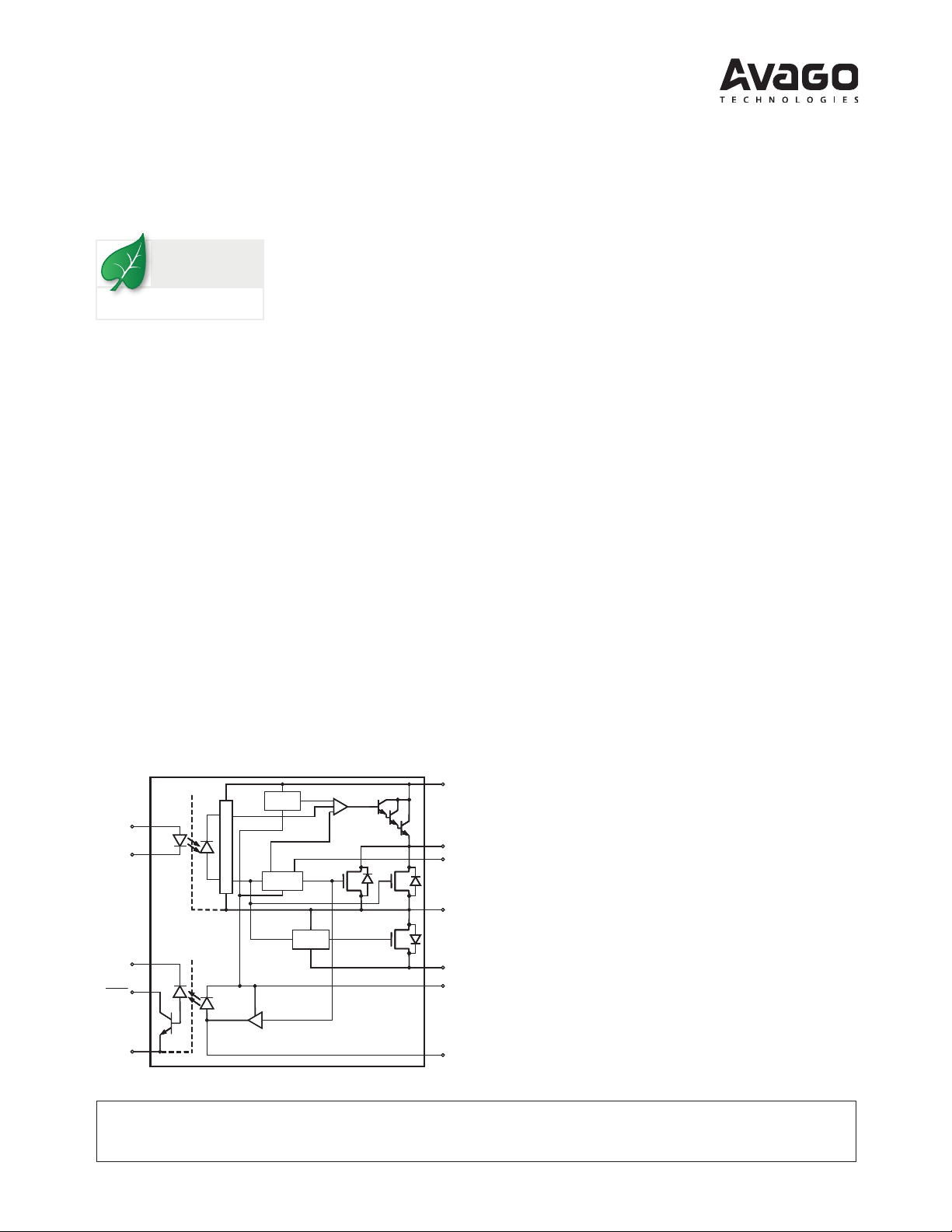
2.5 Amp Output Current IGBT Gate Driver Optocoupler
with Integrated (VCE) Desaturation Detection, UVLO
Fault Status Feedback and Active Miller Clamping
Data Sheet
Description
The ACPL-332J is an advanced 2.5 A output current,
easy-to-use, intelligent gate driver which makes IGBT
VCE fault protection compact, aordable, and easy-to
implement. Features such as integrated VCE detection,
under voltage lockout (UVLO), “soft” IGBT turn-o, isolated
open collector fault feedback and active Miller clamping
provide maximum design exibility and circuit protection.
The ACPL-332J contains a GaAsP LED. The LED is optically
coupled to an integrated circuit with a power output
stage. ACPL-332J is ideally suited for driving power IGBTs
and MOSFETs used in motor control inverter applications.
The voltage and current supplied by these optocouplers
make them ideally suited for directly driving IGBTs with
ratings up to 1200 V and 150 A. For IGBTs with higher
ratings, the ACPL-332J can be used to drive a discrete
power stage which drives the IGBT gate. The ACPL-332J
has an insulation voltage of V
Block Diagram
Features
• Under Voltage Lock-Out Protection (UVLO) with
Hysteresis
• Desaturation Detection
• Miller Clamping
• Open Collector Isolated fault feedback
• “Soft” IGBT Turn-o
• Fault Reset by next LED turn-on (low to high) after
fault mute period
• Available in SO-16 package
• Safety approvals: UL approved, 3750 V
CSA approved, IEC/EN/DIN-EN 60747-5-2 approved
V
= 891 V
IORM
PEAK
Specications
• 2.5 A maximum peak output current
= 891 V
IORM
CAUTION: It is advised that normal static precautions be taken in handling and assembly
of this component to prevent damage and/or degradation which may be induced by ESD.
PEAK
.
• 2.0 A minimum peak output current
• 250 ns maximum propagation delay over temperature
range
• 100 ns maximum pulse width distortion (PWD)
• 15 kV/µs minimum common mode rejection (CMR) at
VCM = 1500 V
• I
< 5 mA maximum supply current
CC(max)
• Wide VCC operating range: 15 V to 30 V over
temperature range
• 1.7 A Miller Clamp. Clamp pin short to VEE if not used
• Wide operating temperature range: –40°C to 100°C
Applications
• Isolated IGBT/Power MOSFET gate drive
• AC and brushless DC motor drives
• Industrial inverters and Uninterruptible Power Supply
(UPS)
for 1 minute,
RMS
Page 2
Pin Description
1
2
3
4
5
6
7
8
16
15
14
13
12
11
10
9
V
E
V
LED
DESAT
V
CC2
V
EE
V
OUT
V
CLAMP
V
EE
V
S
V
CC1
FAULT
V
S
CATHODE
ANODE
ANODE
CATHODE
1
2
3
4
5
6
7
8
16
15
14
13
12
11
10
9
V
E
V
LED
DESAT
V
CC2
V
EE
V
OUT
V
CLAMP
V
EE
V
S
V
CC1
FAULT
V
S
CATHODE
ANODE
ANODE
CATHODE
Pin Symbol Description
1 V
2 V
S
CC1
3 FAULT Fault output. FAULT changes from a high impedance state
4 V
S
5 CATHODE Cathode
6 ANODE Anode
7 ANODE Anode
8 CATHODE Cathode
9 V
10 V
11 V
12 V
13 V
EE
CLAMP
OUT
EE
CC2
14 DESAT Desaturation voltage input. When the voltage on DESAT
15 V
16 V
LED
E
Input Ground
Positive input supply voltage. (4.5 V to 5.5 V)
to a logic low output within 5 µs of the voltage on the
DESAT pin exceeding an internal reference voltage of 7 V.
FAULT output is an open collector which allows the FAULT
outputs from all ACPL-332J in a circuit to be connected
together in a “wired OR” forming a single fault bus for interfacing directly to the micro-controller.
Input Ground
Output supply voltage.
Miller clamp
Gate drive voltage output
Output supply voltage.
Positive output supply voltage
exceeds an internal reference voltage of 6.5 V while the
IGBT is on, FAULT output is changed from a high impedance
state to a logic low state within 5 µs.
LED anode. This pin must be left unconnected for guaranteed data sheet performance. (For optical coupling testing
only)
Common (IGBT emitter) output supply voltage.
Ordering Information
ACPL-332J is UL Recognized with 3750 Vrms for 1 minute per UL1577.
Option
Part number
ACPL-332J -000E SO-16 X X 45 per tube
-500E
Package
To order, choose a part number from the part number column and combine with the desired option from the option
column to form an order entry.
Example 1:
ACPL-332J-500E to order product of SO-16 Surface Mount package in Tape and Reel packaging with IEC/EN/DIN EN
60747-5-2 Safety Approval in RoHS compliant.
Example 2:
ACPL-332J-000E to order product of SO-16 Surface Mount package in tube packaging with IEC/EN/DIN EN 60747-5-
2 Safety Approval and RoHS compliant.
Option datasheets are available. Contact your Avago sales representative or authorized distributor for information.
Remarks: The notation ‘#XXX’ is used for existing products, while (new) products launched since 15th July 2001 and
RoHS compliant option will use ‘-XXXE‘.
Surface
Mount Tape& Reel
X X X
IEC/EN/DIN EN
60747-5-2 QuantityRoHS Compliant
850 per reel
2
Page 3
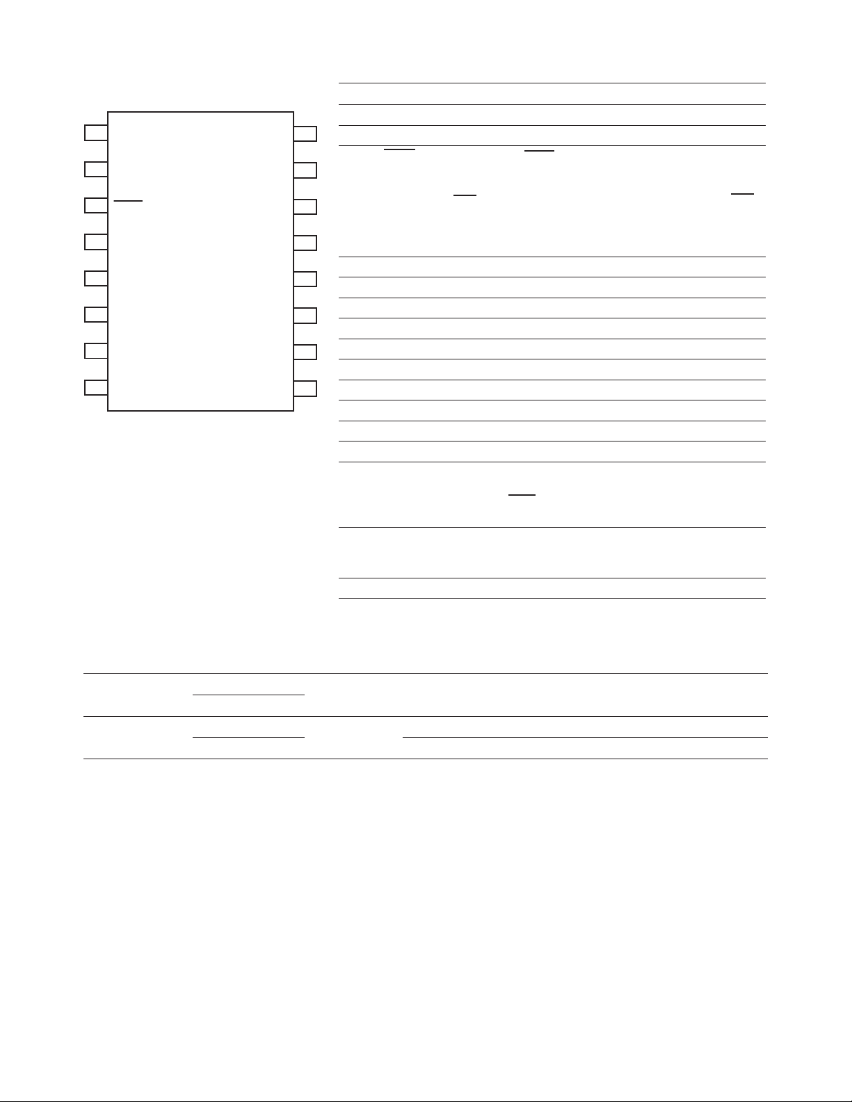
Package Outline Drawings
9
0.295 ± 0.010
(7.493 ± 0.254)
10111213141516
87654321
0.018
(0.457)
0.138 ± 0.005
(3.505 ± 0.127)
9°
0.406 ± 0.10
(10.312 ± 0.254)
0.408 ± 0.010
(10.363 ± 0.254)
0.025 MIN.
0.008 ± 0.003
(0.203 ± 0.076)
STANDOFF
0.345 ± 0.010
(8.763 ± 0.254)
0- 8 °
0.018
(0.457)
0.050
(1.270)
ALL LEADS
TO BE
COPLANAR
± 0.002
A 332J
YYWW
TYPE NUMBER
DATE CODE
0.458 (11.63)
0.085 (2.16)
0.025 (0.64)
LAND PATTERN RECOMMENDATION
ACPL-332J 16-Lead Surface Mount Package
Dimensions in inches (millimeters)
Notes: Initial and continued variation in the color of the ACPL-332J’s white mold compound is normal and does note aect device performance or
reliability.
Floating Lead Protrusion is 0.25 mm (10 mils) max.
3
Page 4
Solder Reow Thermal Prole
0
TIME (SECONDS)
TEMPERATURE ( °C)
200
100
50 150100 200 250
300
0
30
SEC.
50 SEC.
30
SEC.
160 °C
140 °C
150 °C
PEAK
TEMP.
245°C
PEAK
TEMP.
240 °C
PEAK
TEMP.
230 °C
SOLDERING
TIME
200 °C
PREHEATING TIME
150 °C, 90 + 30 SEC.
2.5 °C ± 0.5 °C/SEC.
3°C + 1 °C/ - 0.5 °C
TIGHT
TYPICAL
LOOSE
ROOM
TEMPERATURE
PREHEATING RATE 3 °C + 1 °C/ - 0.5 ° C/SEC.
REFLOW HEATING RATE 2.5°C ± 0.5°C/SEC.
217 °C
RAMP-DOWN
6 °C/SEC. MAX.
RAMP-UP
3 °C/SEC. MAX.
150 - 200 °C
260 +0/-5 °C
t 25 °C to PEAK
60 to 150 SEC.
20-40 SEC.
TIME WITHIN 5°C of ACTUAL
PEAK TEMPERATURE
t
p
t
s
PREHEAT
60 to 180 SEC.
t
L
T
L
T
smax
T
smin
25
T
p
TIME
TEMPERATURE
NO TES:
THE TIME FROM 25°C to PEAK TEMPERATURE = 8 MINUTES MAX.
T
smax
= 200 °C, T
smin
= 150 °C
Note: Non-halide ux should be used.
Recommended Pb-Free IR Prole
Note: Non-halide ux should be used.
4
Page 5

Regulatory Information
The ACPL-332J is approved by the following organizations:
IEC/EN/DIN EN 60747-5-2
Approval under:
IEC 60747-5-2 :1997 + A1:2002
EN 60747-5-2:2001 + A1:2002
DIN EN 60747-5-2 (VDE 0884 Teil 2):2003-01
UL
Approval under UL 1577, component recognition
program up to V
= 3750 V
ISO
. File E55361.
RMS
CSA
Approval under CSA Component Acceptance Notice #5,
File CA 88324.
Table 1. IEC/EN/DIN EN 60747-5-2 Insulation Characteristics*
Description Symbol Characteristic Unit
Installation classication per DIN VDE 0110/1.89, Table 1
for rated mains voltage ≤ 150 V
for rated mains voltage ≤ 300 V
for rated mains voltage ≤ 600 V
rms
rms
rms
Climatic Classication 55/100/21
Pollution Degree (DIN VDE 0110/1.89) 2
Maximum Working Insulation Voltage V
Input to Output Test Voltage, Method b**,
V
x 1.875=VPR, 100% Production Test with tm=1 sec, Partial discharge < 5 pC
IORM
Input to Output Test Voltage, Method a**,
V
x 1.5=VPR, Type and Sample Test, tm=60 sec, Partial discharge < 5 pC
IORM
Highest Allowable Overvoltage (Transient Overvoltage t
= 10 sec) V
ini
V
V
IORM
PR
PR
IOTM
Safety-limiting values – maximum values allowed in the event of a failure.
Case Temperature T
Input Current I
Output Power P
Insulation Resistance at TS, VIO = 500 V R
S
S, INPUT
S, OUTPUT
S
I – IV
I – IV
I – III
891 V
1670 V
1336 V
6000 V
175
400 mA
1200 mW
9
>10
peak
peak
peak
peak
°C
W
* Isolation characteristics are guaranteed only within the safety maximum ratings which must be ensured by protective circuits in application.
Surface mount classication is class A in accordance with CECCOO802.
** Refer to the optocoupler section of the Isolation and Control Components Designer’s Catalog, under Product Safety Regulations section IEC/EN/
DIN EN 60747-5-2, for a detailed description of Method a and Method b partial discharge test proles.
Dependence of Safety Limiting Values on Temperature. (take from DS AV01-0579EN Pg.7)
5
Page 6

Table 2. Insulation and Safety Related Specications
Parameter Symbol ACPL-332J Units Conditions
Minimum External Air Gap
(Clearance)
Minimum External Tracking
(Creepage)
Minimum Internal Plastic Gap
(Internal Clearance)
Tracking Resistance
(Comparative Tracking Index)
Isolation Group IIIa Material Group (DIN VDE 0110, 1/89, Table 1)
L(101) 8.3 Mm Measured from input terminals to output terminals,
shortest distance through air.
L(102) 8.3 Mm Measured from input terminals to output terminals,
shortest distance path along body.
0.5 Mm Through insulation distance conductor to conductor,
usually the straight line distance thickness between
the emitter and detector.
CTI >175 V DIN IEC 112/VDE 0303 Part 1
Table 3. Absolute Maximum Ratings
Parameter Symbol Min. Max. Units Note
Storage Temperature T
Operating Temperature T
Output IC Junction Temperature T
Average Input Current I
Peak Transient Input Current,
S
A
J
F(AVG)
I
F(TRAN)
(<1 µs pulse width, 300pps)
Reverse Input Voltage V
“High” Peak Output Current I
“Low” Peak Output Current I
Positive Input Supply Voltage V
FAULT Output Current I
FAULT Pin Voltage V
Total Output Supply Voltage (V
R
OH(PEAK)
OL(PEAK)
CC1
FAULT
FAULT
- VEE) -0.5 33 V
CC2
Negative Output Supply Voltage (VE - VEE) -0.5 15 V 6
Positive Output Supply Voltage (V
Gate Drive Output Voltage V
Peak Clamping Sinking Current I
Miller Clamping Pin Voltage V
DESAT Voltage V
Output IC Power Dissipation P
Input IC Power Dissipation P
- VE) -0.5 33 - (VE - VEE) V
CC2
O(PEAK)
Clamp
Clamp
DESAT
O
I
Solder Reow Temperature Prole See Package Outline Drawings section
-55 125 °C
-40 100 °C 2
125 °C 2
25 mA 1
1.0 A
5 V
2.5 A 3
2.5 A 3
-0.5 5.5 V
8.0 mA
-0.5 V
-0.5 V
CC1
CC2
V
V
1.7 A
-0.5 V
V
E
CC2
VE + 10 V
V
600 mW 2
150 mW 2
Table 4. Recommended Operating Conditions
Parameter Symbol Min. Max. Units Note
Operating Temperature T
Total Output Supply Voltage (V
A
- VEE) 15 30 V 7
CC2
Negative Output Supply Voltage (VE - VEE) 0 15 V 4
Positive Output Supply Voltage (V
Input Current (ON) I
Input Voltage (OFF) V
- VE) 15 30 - (VE - VEE) V
CC2
F(ON)
F(OFF)
6
- 40 100 °C 2
8 12 mA
- 3.6 0.8 V
Page 7
Table 5. Electrical Specications (DC)
Unless otherwise noted, all typical values at TA = 25°C, V
- VEE = 30 V, VE - VEE = 0 V;
CC2
all Minimum/Maximum specications are at Recommended Operating Conditions. Positive Supply Voltage used.
Parameter Symbol Min. Typ. Max. Units Test Conditions Fig. Note
FAULT Logic Low Output
Voltage
FAULT Logic High Output
Current
High Level
Output Current
Low Level
Output Current
Low Level Output Current
During Fault Condition
High Level Output Voltage V
Low Level Output Voltage V
Clamp Pin Threshold Voltage V
Clamp Low Level
Sinking Current
High Level Supply Current I
Low Level Supply Current I
Blanking Capacitor
Charging Current
Blanking Capacitor
Discharge Current
DESAT Threshold V
UVLO Threshold V
UVLO Hysteresis (V
Threshold Input Current
Low to High
Threshold Input Voltage
High to Low
Input Forward Voltage V
Temperature Coecient
of Input Forward Voltage
Input Reverse Breakdown
Voltage
Input Capacitance C
V
FAULTL
I
FAULTH
I
OH
I
OL
I
OLF
OH
OL
tClamp
I
CL
CC2H
CC2L
I
CHG
I
DSCHG
DESAT
UVLO+
V
UVLO-
UVLO+
- V
UVLO-
I
FLH
V
FHL
F
DVF/DT
BV
R
IN
0.1 V I
0.1 V I
0.003 µA V
0.003 µA V
-0.5 -1.5 A VO = V
-2.0 A VO = V
FAULT
FAULT
FAULT
FAULT
= 1.1 mA, V
= 1.1 mA, V
= 5.5 V, V
= 3.3 V, V
- 4 2, 4, 215
CC2
– 15 3
CC2
CC1
CC1
CC1
CC1
= 5.5V
= 3.3V
= 5.5V
= 3.3V
0.5 1.5 A VO = VEE + 2.5 3, 5, 225
2.0 A VO = VEE + 15 3
90 140 230 mA V
- VEE = 14 V 6
OUT
VCC-3.5 VCC-2.5 V IO = 100 mA 4, 6, 237, 8, 9
VCC-2.9 VCC-2.0 V IO = -650 µA 23
0.17 0.5 V IO = 100 mA 5, 7,
24
2.0 V
0.35 1.1 A VO = VEE + 2.5 8
2.5 5 mA IO = 0 mA 9, 10,
2.5 5 mA IO = 0 mA
-0.13 -0.24 -0.33 mA V
10 30 mA V
6 6.5 7.5 V V
= 2 V 11, 27 9, 10
DESAT
= 7.0 V 28
DESAT
-VE >V
CC2
UVLO-
25,
26
12 9
10.5 11.6 12.5 V VO > 5 V 7, 9,
9.2 10.3 11.1 V VO < 5 V 7, 9,
0.4 1.3 V
)
2.0 8 mA IO = 0 mA, VO > 5 V
0.8 V
1.2 1.6 1.95 V IF = 10 mA
A
5 V
-1.3 mV/°C
IR = 10 mA
70 pF f = 1 MHz, VF = 0 V
9
11
12
7
Page 8

Table 6. Switching Specications (AC)
Unless otherwise noted, all typical values at TA = 25°C, V
- VEE = 30 V, VE - VEE = 0 V;
CC2
all Minimum/Maximum specications are at Recommended Operating Conditions. Only Positive Supply Voltage used.
Parameter Symbol Min. Typ. Max. Units Test Conditions Fig. Note
Propagation Delay Time
to High Output Level
Propagation Delay Time
to Low Output Level
Pulse Width Distortion PWD -100 20 100 ns 14, 17
Propagation Delay
Dierence Between
Any Two Parts or Channels
Rise Time t
Fall Time t
DESAT Sense to
90%VO Delay
DESAT Sense to
10% VO Delay
DESAT Sense to Low Level
FAULT Signal Delay
DESAT Sense to DESAT
Low Propagation Delay
DESAT Input Mute t
RESET to High Level FAULT
Signal Delay
Output High Level Common
Mode Transient Immunity
Output Low Level Common
Mode Transient Immunity
t
PLH
100 180 250 ns
Rg = 10 W,
Cg = 10 nF,
f = 10 kHz,
t
(t
PHL
PHL
- t
100 180 250 ns 1, 13,
)
-350 350 ns 17, 16
PLH
Duty Cycle = 50%,
IF = 10 mA,
V
= 30 V
CC2
PDD
R
F
t
DESAT(90%)
t
DESAT(10%)
t
DESAT(FAULT)
50 ns
50 ns
0.15 0.5 µs
2 3 µs
0.25 0.5 µs
C
= 100pF, Rg = 10 W,
DESAT
Cg = 10 nF, V
C
DESAT
Cg = 10 nF, V
C
DESAT
CC2
= 100pF, Rg = 10 W,
CC2
= 100pF, RF = 2.1 kW,
= 30 V
= 30 V
Rg = 10 W, Cg = 10 nF,
V
= 30 V
CC2
t
DESAT(LOW)
0.25 µs
C
= 100pF, RF = 2.1 kW,
DESAT
Rg = 10 W, Cg = 10 nF,
V
= 30 V
CC2
DESAT(MUTE)
t
RESET(FAULT )
5 µs 37 20
0.3 1 2.0 µs
C
= 100pF, RF = 2.1 kW,
DESAT
Rg = 10 W, Cg = 10 nF,
V
0.8 1.5 2.5 µs
= 5.5V, V
CC1
C
= 100pF, RF = 2.1 kW,
DESAT
CC2
= 30 V
Rg = 10 W, Cg = 10 nF,
V
= 3.3V, V
CC1
CC2
= 30 V
|CMH| 15 25 kV/µs TA = 25°C, IF = 10 mA
VCM = 1500 V, V
CC2
= 30 V
|CML| 15 25 kV/µs TA = 25°C, VF = 0 V
VCM = 1500 V, V
CC2
= 30 V
1, 13,
13, 15
14, 15,
16, 29
14, 15,
16, 29
17, 30, 3719
18, 19,
20, 30,
37
30, 37 18
30, 37 19
31, 32,
21
33, 34
31, 32,
22
33, 34
8
Page 9

Table 7. Package Characteristics
Parameter Symbol Min. Typ. Max. Units Test Conditions Fig. Note
Input-Output Momentary
Withstand Voltage
Input-Output Resistance R
Input-Output Capacitance C
Output IC-to-Pins 9 &10
Thermal Resistance
Notes:
1. Derate linearly above 70°C free air temperature at a rate of 0.3 mA/°C.
2. In order to achieve the absolute maximum power dissipation specied, pins 4, 9, and 10 require ground plane connections and may require
airow. See the Thermal Model section in the application notes at the end of this data sheet for details on how to estimate junction temperature
and power dissipation. In most cases the absolute maximum output IC junction temperature is the limiting factor. The actual power dissipation
achievable will depend on the application environment (PCB Layout, air ow, part placement, etc.). See the Recommended PCB Layout section
in the application notes for layout considerations. Output IC power dissipation is derated linearly at 10 mW/°C above 90°C. Input IC power
dissipation does not require derating.
3. Maximum pulse width = 10 µs. This value is intended to allow for component tolerances for designs with IO peak minimum = 2.0 A. Derate
linearly from 3.0 A at +25°C to 2.5 A at +100°C. This compensates for increased I
4. This supply is optional. Required only when negative gate drive is implemented.
5. Maximum pulse width = 50 µs.
6. See the Slow IGBT Gate Discharge During Fault Condition section in the applications notes at the end of this data sheet for further details.
7. 15 V is the recommended minimum operating positive supply voltage (V
threshold of 12.5V. For High Level Output Voltage testing, VOH is measured with a dc load current. When driving capacitive loads, VOH will
approach VCC as IOH approaches zero units.
8. Maximum pulse width = 1.0 ms.
9. Once VO of the ACPL-332J is allowed to go high (V
IGBT protection. UVLO is needed to ensure DESAT is functional. Once V
DESAT detection and UVLO features of the ACPL-332J work in conjunction to ensure constant IGBT protection.
10. See the DESAT fault detection blanking time section in the applications notes at the end of this data sheet for further details.
11. This is the “increasing” (i.e. turn-on or “positive going” direction) of V
12. This is the “decreasing” (i.e. turn-o or “negative going” direction) of V
13. This load condition approximates the gate load of a 1200 V/150A IGBT.
14. Pulse Width Distortion (PWD) is dened as |t
15. As measured from IF to VO.
16. The dierence between t
17. As measured from ANODE, CATHODE of LED to V
18. This is the amount of time from when the DESAT threshold is exceeded, until the FAULT output goes low.
19. This is the amount of time the DESAT threshold must be exceeded before V
voltage dependent.
20. Auto Reset: This is the amount of time when V
Reset) topic in the application information section.
21. Common mode transient immunity in the high state is the maximum tolerable dVCM/dt of the common mode pulse, VCM, to assure that the
output will remain in the high state (i.e., VO > 15 V or FAULT > 2 V). A 100 pF and a 2.1 kΩ pull-up resistor is needed in fault detection mode.
22. Common mode transient immunity in the low state is the maximum tolerable dVCM/dt of the common mode pulse, VCM, to assure that the
output will remain in a low state (i.e., VO < 1.0 V or FAULT < 0.8 V).
23. To clamp the output voltage at VCC - 3 VBE, a pull-down resistor between the output and VEE is recommended to sink a static current of 650 µA
while the output is high. See the Output Pull-Down Resistor section in the application notes at the end of this data sheet if an output pull-down
resistor is not used.
PHL
and t
V
ISO
3750 V
rms
RH < 50%, t = 1 min.,
TA = 25°C
9
I-O
I-O
q
09-10
CC2
- t
PHL
PLH
between any two ACPL-332J parts under the same test conditions.
PLH
OUT
will be asserted low after DESAT threshold is exceeded. See the Description of Operation (Auto
OUT
> 10
1.3 pF freq=1 MHz
30 °C/W TA = 25°C
- VE > V
| for any given unit.
), the DESAT detection feature of the ACPL-332J will be the primary source of
UVLO
UVLO+
- V
CC2
CC2
W
OPEAK
- VE) to ensure adequate margin in excess of the maximum V
CC2
> 12.5 V, DESAT will remain functional until V
E
- V
E
begins to go low, and the FAULT output to go low. This is supply
OUT
V
I-O
due to changes in VOL over temperature.
= 500 V 7
< 9.2 V. Thus, the
UVLO-
6, 7
UVLO+
9
Page 10

1.0
1.5
2.0
2.5
3.0
-40 -20 0 20 40 60 80 100
TA- TEMPERATURE -oC
I
OH
- OUTPUT HIGH CURRENT - A
0
1
2
3
4
5
-40 -20 0 20 40 60 80 100
TA- TEMPERATURE -oC
I
OL
- OUTPUT LOW CURRENT
-----V
OUT=VEE
+15V
___V
OUT=VEE
+2.5V
-3
-2.5
-2
-1.5
-1
-0.5
0
-40 -20 0 20 40 60 80 100
TA- TEMPERATURE -oC
(V
OH
- V
CC
) - HIGH OUTPUT VOLTAGE DROP - V
------I
OUT
= -100mA
____I
OUT
= -650uA
0
0.05
0.1
0.15
0.2
0.25
-40 -20 0 20 40 60 80 100
TA- TEMPERATURE -oC
V
OL
- OUTPUT LOW VOLTAGE - V
Figure 1. VOUT propagation delay waveforms
I
F
V
OUT
t
PHL
t
PLH
t
f
t
r
10%
50%
90%
Figure 2. IOH vs. temperature Figure 3. IOL vs. temperature
Figure 4. VOH vs. temperature Figure 5. VOL vs. temperature
10
Page 11

0
1
2
3
4
-40 -20 0 20 40 60 80 100
TA-TEMPERATURE-oC
I
CL
- CLAMP LOW LEVEN SINKING CURRENT
15 20 25 30
2.25
2.35
2.45
2.55
2.65
V
CC2
- OUTPUR SUPPLY VOLTAGE - V
I
CC2
- OUTPUT SUPPLY CURRENT - mA
---------I
Cc 2H
_
________
I
CC2L
2.00
2.25
2.50
2.75
3.00
3.25
3.50
-40 -20 0 20 40 60 80 100
TA - TEMPERATURE - oC
I
CC2
- OUTPUT SUPPLY CURRENT - mA
----- ----I
CC2 H
_
________
I
CC2L
-0.35
-0.30
-0.25
-0.20
-40 -20 0 20 40 60 80 100
TA- TEMPERATURE -oC
I
CH
- BLANKING CAPACITOR
CHARGING CURRENT - mA
28.0
28.5
29.0
29.5
30.0
0 0.2 0.4 0.6 0.8 1
IOH - OUTPUT HIGH CURRENT - A
V
OH
- HIGH OUTPUT VOLTAGE DROP - V
_ _ _ _ 100oC
______ 25oC
--------- -40oC
Figure 6. VOH vs. I
0
1
2
3
4
5
6
7
8
0 0.5 1 1.5 2 2.5
IoL - OUTPUT LOW CURRENT - A
V
OL
- LOW OUTPUT VOLTAGE DROP - V
_ _ _ _ 100oC
______ 25oC
--------- -40oC
OH
Figure 7. VOL vs. I
OL
Figure 8. ICL vs. temperature
Figure 10. I
11
vs. V
CC2
CC2
Figure 9. I
Figure 11. I
vs. temperature
CC2
vs. temperature
CHG
Page 12

100
150
200
250
300
15 20 25 30
Vcc - SUPPLY VOLTAGE - V
T
P
- PROPAGATION DELAY - ns
----------t
PLH
_______t
PHL
100
150
200
250
300
0 10 20 30 40 50
LOAD RESISTANCE - ohm
T
P
- PROPAGATION DELAY - ms
----------t
PLH
_______t
PHL
0
100
200
300
0 10 20 30 40 50
LOAD CAPACITANCE - nF
----------t
PLH
_______t
PHL
T
P
- PROPAGATION DELAY - ms
Figure 12. DESAT threshold vs. temperature
6.0
6.5
7.0
7.5
-40 -20 0 20 40 60 80 100
TA- TEMPERATURE -oC
V
DESAT
- DESAT THRESHOLD - V
100
150
200
250
300
-40 -20 0 20 40 60 80 100
TA- TEMPERATURE -oC
T
P
- PROPAGATION DELAY - ns
----------t
PLH
_______t
PHL
Figure 13. Propagation delay vs. temperature
Figure 14. Propagation delay vs. supply voltage
Figure 16. Propagation delay vs. load capacitance
12
Figure 15. Propagation delay vs. load resistance
Page 13

1.0
1.5
2.0
2.5
3.0
-40 -20 0 20 40 60 80 100
TA- TEMPERATURE -oC
T
DESAT
- DESAT Sense to 10% Vo Delay - us
-------V
cc2
=15V
_____V
cc2
=30V
0.0
1.0
2.0
3.0
4.0
10 20 30 40 50
LOAD RESISTANCE - ohm
-------V
cc2
=15V
_____V
cc2
=30V
T
DESAT10%
- DESAT Sense to 10% Vo Delay - us
0.000
0.004
0.008
0.012
0 10 20 30 40 50
LOAD CAPACITANCE - nF
-------V
cc2
=15V
_____V
cc2
=30V
T
DESAT10%
- DESAT Sense to 10% Vo Delay - ms
100
150
200
250
300
-40 -20 0 20 40 60 80 100
TA- TEMPERATURE -oC
T
DESAT90%
- DESAT Sense to 90% Vo Delay - ns
Figure 17. DESAT sense to 90% VOUT delay vs. temperature
Figure 18. DESAT sense to 10% VOUT delay vs. temperature
Figure 19. DESAT sense to 10% VOUT delay vs. load resistance
13
Figure 20. DESAT sense to 10% VOUT delay vs. load capacitance
Page 14

Figure 21. IOH Pulsed test circuit
1
2
3
4
5
6
7
8
16
15
14
13
12
11
10
9
V
E
V
LED
DESAT
V
CC2
V
EE
V
OUT
V
CLAMP
V
EE
V
S
V
CC1
FAULT
V
S
CATHODE
ANODE
ANODE
CATHODE
+
_
10mA
+
_
0.1µF
0.1µF
15V Pulsed
I
OUT
30V
1
2
3
4
5
6
7
8
16
15
14
13
12
11
10
9
V
E
V
LED
DESAT
V
CC2
V
EE
V
OUT
V
CLAMP
V
EE
V
S
V
CC1
V
S
CATHODE
ANODE
ANODE
CATHODE
+
_
10mA
+
_
0.1µF0.1µF
0.1µF0.1µF
15V Pulsed
I
OUT
30V
1
2
3
4
5
6
7
8
16
15
14
13
12
11
10
9
V
E
V
LED
DESAT
V
CC2
V
EE
V
OUT
V
CLAMP
V
EE
V
S
V
CC1
FAULT
V
S
CATHODE
ANODE
ANODE
CATHODE
+
_
+
_
0.1µF
0.1µF
15V Pulsed
I
OUT
30V
+
_
0.1µF
0.1µF
1
2
3
4
5
6
7
8
16
15
14
13
12
11
10
9
V
E
V
LED
DESAT
V
CC2
V
EE
V
OUT
V
CLAMP
V
EE
V
S
V
CC1
FAULT
V
S
CATHODE
ANODE
ANODE
CATHODE
+
_
0.1µF
0.1µF
100mA
V
OUT
30V
10mA
1
2
3
4
5
6
7
8
16
15
14
13
12
11
10
9
V
E
V
LED
DESAT
V
CC2
V
EE
V
OUT
V
CLAMP
V
EE
V
S
V
CC1
V
S
CATHODE
ANODE
ANODE
CATHODE
+
_
0.1µF0.1µF
0.1µF0.1µF
100mA
V
OUT
30V
10mA10mA
Figure 22. IOL Pulsed test circuit
Figure 23. VOH Pulsed test circuit
14
Page 15

Figure 24. VOL Pulsed test circuit
1
2
3
4
5
6
7
8
16
15
14
13
12
11
10
9
V
E
V
LED
DESAT
V
CC2
V
EE
V
OUT
V
CLAMP
V
EE
V
S
V
CC1
FAULT
V
S
CATHODE
ANODE
ANODE
CATHODE
+
_
0.1µF
0.1µF
100mA
V
OUT
30V
1
2
3
4
5
6
7
8
16
15
14
13
12
11
10
9
V
E
V
LED
DESAT
V
CC2
V
EE
V
OUT
V
CLAMP
V
EE
V
S
V
CC1
FAULT
V
S
CATHODE
ANODE
ANODE
CATHODE
+
_
0.1µF0.1µF
0.1µF0.1µF
100mA
V
OUT
30V
1
2
3
4
5
6
7
8
16
15
14
13
12
11
10
9
V
E
V
LED
DESAT
V
CC2
V
EE
V
OUT
V
CLAMP
V
EE
V
S
V
CC1
FAULT
V
S
CATHODE
ANODE
ANODE
CATHODE
+
_
0.1µF
0.1µF
I
CC2
30V
10mA
1
2
3
4
5
6
7
8
16
15
14
13
12
11
10
9
V
E
V
LED
DESAT
V
CC2
V
EE
V
OUT
V
CLAMP
V
EE
V
S
V
CC1
FAULT
V
S
CATHODE
ANODE
ANODE
CATHODE
+
_
0.1µF0.1µF
0.1µF0.1µF
I
CC2
30V
10mA10mA
1
2
3
4
5
6
7
8
16
15
14
13
12
11
10
9
V
E
V
LED
DESAT
V
CC2
V
EE
V
OUT
V
CLAMP
V
EE
V
S
V
CC1
FAULT
V
S
CATHODE
ANODE
ANODE
CATHODE
+
_
0.1µF
0.1µF
30V
I
CC2
1
2
3
4
5
6
7
8
16
15
14
13
12
11
10
9
V
E
V
LED
DESAT
V
CC2
V
EE
V
OUT
V
CLAMP
V
EE
V
S
V
CC1
V
S
CATHODE
ANODE
ANODE
CATHODE
+
_
0.1µF0.1µF
0.1µF0.1µF
30V
I
CC2
Figure 25. I
Figure 26. I
15
CC2H
CC2L
test circuit
test circuit
Page 16

Figure 27. I
1
2
3
4
5
6
7
8
16
15
14
13
12
11
10
9
V
E
V
LED
DESAT
V
CC2
V
EE
V
OUT
V
CLAMP
V
EE
V
S
V
CC1
FAULT
V
S
CATHODE
ANODE
ANODE
CATHODE
+
_
0.1µF
0.1µF
I
CHG
30V
10mA
1
2
3
4
5
6
7
8
16
15
14
13
12
11
10
9
V
E
V
LED
DESAT
V
CC2
V
EE
V
OUT
V
CLAMP
V
EE
V
S
V
CC1
FAULT
V
S
CATHODE
ANODE
ANODE
CATHODE
+
_
0.1µF
0.1µF
I
CHG
30V
10mA10mA
1
2
3
4
5
6
7
8
16
15
14
13
12
11
10
9
V
E
V
LED
DESAT
V
CC2
V
EE
V
OUT
V
CLAMP
V
EE
V
S
V
CC1
FAULT
V
S
CATHODE
ANODE
ANODE
CATHODE
+
_
0.1µF
0.1µF
7V
30V
+
_
IDSCHG
1
2
3
4
5
6
7
8
16
15
14
13
12
11
10
9
V
E
V
LED
DESAT
V
CC2
V
EE
V
OUT
V
CLAMP
V
EE
V
S
V
CC1
FAULT
V
S
CATHODE
ANODE
ANODE
CATHODE
+
_
0.1µF
0.1µF
7V
30V
+
_
IDSCHG
10nF
1
2
3
4
5
6
7
8
16
15
14
13
12
11
10
9
V
E
V
LED
DESAT
V
CC2
V
EE
V
OUT
V
CLAMP
V
EE
V
S
V
CC1
FAULT
V
S
CATHODE
ANODE
ANODE
CATHODE
+
_
0.1µF
0.1µF
V
OUT
30V
10Ω
10mA, 10kHz,
50% Duty Cycle
10nF10nF
1
2
3
4
5
6
7
8
16
15
14
13
12
11
10
9
V
E
V
LED
DESAT
V
CC2
V
EE
V
OUT
V
CLAMP
V
EE
V
S
V
CC1
FAULT
V
S
CATHODE
ANODE
ANODE
CATHODE
+
_
0.1µF0.1µF
V
OUT
30V
10mA, 10kHz,
50% Duty Cycle
Pulsed test circuit
CHG
Figure 28. I
Figure 29. t
16
DSCHG
, t
PLH
test circuit
, tf, tr, test circuit
PHL
Page 17

V
CM
10
10nF
1
2
3
4
5
6
7
8
16
15
14
13
12
11
10
9
V
E
V
LED
DESAT
V
CC2
V
EE
V
OUT
V
CLAMP
V
EE
V
S
V
CC1
FAULT
V
S
CATHODE
ANODE
ANODE
CATHODE
0.1µF
SCOPE
30V
430Ω
2.1kΩ
0.1µF
15pF
5V
V
CM
10Ω
10nF10nF
1
2
3
4
5
6
7
8
16
15
14
13
12
11
10
9
V
E
V
LED
DESAT
V
CC2
V
EE
V
OUT
V
CLAMP
V
EE
V
S
V
CC1
FAULT
V
S
CATHODE
ANODE
ANODE
CATHODE
0.1µF0.1µF
SCOPE
30V
0.1µF0.1µF
15pF15pF
5V5V
V
CM
10Ω
10nF
1
2
3
4
5
6
7
8
16
15
14
13
12
11
10
9
V
E
V
LED
DESAT
V
CC2
V
EE
V
OUT
V
CLAMP
V
EE
V
S
V
CC1
FAULT
V
S
CATHODE
ANODE
ANODE
CATHODE
0.1µF
SCOPE
30V
430Ω
2.1kΩ
0.1µF
15pF
5V
V
CM
10nF10nF
1
2
3
4
5
6
7
8
16
15
14
13
12
11
10
9
V
E
V
LED
DESAT
V
CC2
V
EE
V
OUT
V
CLAMP
V
EE
V
S
V
CC1
FAULT
V
S
CATHODE
ANODE
ANODE
CATHODE
0.1µF0.1µF
SCOPE
30V
0.1µF0.1µF
15pF15pF
5V5V
Figure 30. t
10nF
+
_
1
2
3
4
5
6
7
8
16
15
14
13
12
11
10
9
V
E
V
LED
DESAT
V
CC2
V
EE
V
OUT
V
CLAMP
V
EE
V
S
V
CC1
FAULT
V
S
CATHODE
ANODE
ANODE
CATHODE
+
_
5V
0.1µF
0.1µF
V
OUT
30V
10Ω
V
IN
2.1kΩ
V
FAULT
10mA
10nF
+
_
1
2
3
4
5
6
7
8
16
15
14
13
12
11
10
9
V
E
V
LED
DESAT
V
CC2
V
EE
V
OUT
V
CLAMP
V
EE
V
S
V
CC1
V
S
CATHODE
ANODE
ANODE
CATHODE
+
_
5V
0.1µF0.1µF
0.1µF0.1µF
V
OUT
30V
V
IN
V
FAULT
10mA10mA
fault test circuit
DESAT
Figure 31. CMR Test circuit LED2 o
Figure 32. CMR Test Circuit LED2 on
17
Page 18

10
10nF
1
2
3
4
5
6
7
8
16
15
14
13
12
11
10
9
V
E
V
LED
DESAT
V
CC2
V
EE
V
OUT
V
CLAMP
V
EE
V
S
V
CC1
FAULT
V
S
CATHODE
ANODE
ANODE
CATHODE
0.1µF
SCOPE
30V
V
CM
430Ω
2.1kΩ
0.1µF
15pF
5V
1010Ω
10nF10nF
0.1µF0.1µF
SCOPE
30V
V
CM
10
10nF
1
2
3
4
5
6
7
8
16
15
14
13
12
11
10
9
V
E
V
LED
DESAT
V
CC2
V
EE
V
OUT
V
CLAMP
V
EE
V
S
V
CC1
FAULT
V
S
CATHODE
ANODE
ANODE
CATHODE
0.1µF
SCOPE
30V
430
2.1k
0.1µF
15pF
5V
SCOPE
2.1kΩ
0.1µF
15pF
5V
Ω
Ω
Figure 33. CMR Test circuit LED1 o
Figure 34. CMR Test Circuit LED1 on
18
Page 19

SHIELD
SHIELD
D
R
I
V
E
R
V
E
DESAT
V
CC2
V
OUT
V
CLAMP
V
EE
V
CC1
V
S
FAULT
ANODE
CATHODE
V
CLAMP
V
LED
6, 7
5, 8
2
3
1, 4
13
11
14
9, 12
10
16
15
DESAT
UVLO
LED1
LED2
SHIELD
SHIELD
D
R
I
V
E
R
V
E
DESAT
V
CC2
V
OUT
V
CLAMP
V
EE
V
CC1
V
S
FAULT
ANODE
CATHODE
V
CLAMP
V
LED
6, 7
5, 8
2
3
1, 4
13
11
14
9, 12
10
16
15
DESAT
UVLO
LED1
LED2
Application Information
Product Overview Description
The ACPL-332J is a highly integrated power control device
that incorporates all the necessary components for a
complete, isolated IGBT / MOSFET gate drive circuit with
fault protection and feedback into one SO-16 package.
Active Miller clamp function eliminates the need of
negative gate drive in most application and allows the
use of simple bootstrap supply for high side driver. An
optically isolated power output stage drives IGBTs with
power ratings of up to 150 A and 1200 V. A high speed
internal optical link minimizes the propagation delays
between the microcontroller and the IGBT while allowing
the two systems to operate at very large common mode
voltage dierences that are common in industrial motor
drives and other power switching applications. An output
IC provides local protection for the IGBT to prevent
damage during over current, and a second optical link
provides a fully isolated fault status feedback signal for
the microcontroller. A built in “watchdog” circuit, UVLO
monitors the power stage supply voltage to prevent IGBT
caused by insucient gate drive voltages. This integrated
IGBT gate driver is designed to increase the performance
and reliability of a motor drive without the cost, size, and
complexity of a discrete design.
Two light emitting diodes and two integrated circuits
housed in the same SO-16 package provide the input
control circuitry, the output power stage, and two optical
channels. The output Detector IC is designed manufactured on a high voltage BiCMOS/Power DMOS process.
The forward optical signal path, as indicated by LED1,
transmits the gate control signal. The return optical signal
path, as indicated by LED2, transmits the fault status
feedback signal.
Under normal operation, the LED1 directly controls the
IGBT gate through the isolated output detector IC, and
LED2 remains o. When an IGBT fault is detected, the
output detector IC immediately begins a “soft” shutdown
sequence, reducing the IGBT current to zero in a controlled manner to avoid potential IGBT damage from
inductive over voltages. Simultaneously, this fault status
is transmitted back to the input via LED2, where the fault
latch disables the gate control input and the active low
fault output alerts the microcontroller.
During power-up, the Under Voltage Lockout (UVLO)
feature prevents the application of insucient gate
voltage to the IGBT, by forcing the ACPL-332J’s output
low. Once the output is in the high state, the DESAT (VCE)
detection feature of the ACPL-332J provides IGBT protection. Thus, UVLO and DESAT work in conjunction to
provide constant IGBT protection.
19
Figure 35. Block Diagram of ACPL-332J
Recommended Application Circuit
The ACPL-332J has an LED input gate control, and an
open collector fault output suitable for wired ‘OR’ applications. The recommended application circuit shown
in Figure 36 illustrates a typical gate drive implementation using the ACPL-332J. The following describes about
driving IGBT. However, it is also applicable to MOSFET.
Depending upon the MOSFET or IGBT gate threshold requirements, designers may want to adjust the VCC supply
voltage (Recommended VCC = 17.5V for IGBT and 12.5V
for MOSFET).
The two supply bypass capacitors (0.1 µF) provide the
large transient currents necessary during a switching
transition. Because of the transient nature of the charging
currents, a low current (5mA) power supply suces. The
desaturation diode D
trr below 75ns (e.g. ERA34-10) and capacitor C
necessary external components for the fault detection
circuitry. The gate resistor RG serves to limit gate charge
current and controls the IGBT collector voltage rise
and fall times. The open collector fault output has a
passive pull-up resistor RF (2.1 kW) and a 330 pF ltering
capacitor, CF. A 47 kW pull down resistor R
V
provides a predictable high level output voltage
OUT
(VOH). In this application, the IGBT gate driver will shut
down when a fault is detected and fault reset by next
cycle of IGBT turn on. Application notes are mentioned at
the end of this datasheet.
600V/1200V fast recovery type,
DESAT
PULL-DOWN
BLANK
are
on
Page 20

Figure 36. Recommended application circuit (Single Supply) with desaturation detection and active Miller Clamp
+
_
+
_
1
2
3
4
5
6
7
8
16
15
14
13
12
11
10
9
V
E
V
LED
DESAT
V
CC2
V
EE
V
OUT
V
CLAMP
V
EE
V
S
V
CC1
FAULT
V
S
CATHODE
ANODE
ANODE
CATHODE
+
_
R
G
100 Ω
C
BLANK
D
DESAT
Q1
Q2
+
V
CE
-
R
F
R
R
PULL-DOWN
+ HVDC
- HVDC
3-PHASE
AC
+
V
CE
-
0.1µF 0.1µF
0.1µF
C
F
7
+
_
-
I
F
V
DESAT
V
OUT
FAULT
6.5V
50%
t
DESAT(LOW)
10%
t
DESAT(10%)
90%
t
DESAT(90%)
50%
t
DESAT(FAULT)
t
DESAT(MUTE))
50%
t
RESET(FAULT)
Reset done
during the
next LED
turn-on
I
F
V
DESAT
V
OUT
FAULTFAULT
6.5V
50%
t
DESAT(LOW)
10%
t
DESAT(10%)
90%
t
DESAT(90%)
50%
t
DESAT(FAULT)
t
DESAT(MUTE))
50%
t
RESET(FAULT)
Reset done
during the
next LED
turn-on
Description of Operation
Normal Operation
During normal operation, V
of the ACPL-332J is con-
OUT
trolled by input LED current IF (pins 5, 6, 7 and 8), with
the IGBT collector-to-emitter voltage being monitored
through DDESAT. The FAULT output is high. See Figure 37.
Fault Condition
The DESAT pin monitors the IGBT Vce voltage. When the
voltage on the DESAT pin exceeds 6.5 V while the IGBT is
on, V
the IGBT and prevent large di/dt induced voltages. Also
Figure 37. Fault Timing diagram
20
is slowly brought low in order to “softly” turn-o
OUT
activated is an internal feedback channel which brings
the FAULT output low for the purpose of notifying the
micro-controller of the fault condition.
Fault Reset
Once fault is detected, the output will be muted for 5 µs
(minimum). All input LED signals will be ignored during
the mute period to allow the driver to completely soft
shut-down the IGBT. The fault mechanism can be reset by
the next LED turn-on after the 5us (minimum) mute time.
See Figure 37.
Page 21

Output Control
Slow IGBT Gate Discharge during Fault Condition
The outputs (V
and FAULT) of the ACPL-332J are con-
OUT
trolled by the combination of IF, UVLO and a detected
IGBT Desat condition. Once UVLO is not active (V
> V
), VOUT is allowed to go high, and the DESAT (pin
UVLO
CC2
- VE
14) detection feature of the ACPL-332J will be the primary
source of IGBT protection. UVLO is needed to ensure
DESAT is functional. Once V
remain functional until V
UVLO-
> 10.5 V, DESAT will
UVLO+
< 11.1 V. Thus, the DESAT
detection and UVLO features of the ACPL-332J work in
conjunction to ensure constant IGBT protection.
Desaturation Detection and High Current Protection
The ACPL-332J satises these criteria by combining a high
speed, high output current driver, high voltage optical
isolation between the input and output, local IGBT desaturation detection and shut down, and an optically
isolated fault status feedback signal into a single 16-pin
surface mount package.
The fault detection method, which is adopted in the
ACPL-332J, is to monitor the saturation (collector)
voltage of the IGBT and to trigger a local fault shutdown
sequence if the collector voltage exceeds a predetermined threshold. A small gate discharge device slowly
reduces the high short circuit IGBT current to prevent
damaging voltage spikes. Before the dissipated energy
can reach destructive levels, the IGBT is shut o. During
the o state of the IGBT, the fault detect circuitry is simply
disabled to prevent false ‘fault’ signals.
The alternative protection scheme of measuring IGBT
current to prevent desaturation is eective if the short
circuit capability of the power device is known, but
this method will fail if the gate drive voltage decreases
enough to only partially turn on the IGBT. By directly
measuring the collector voltage, the ACPL-332J limits the
power dissipation in the IGBT even with insucient gate
drive voltage. Another more subtle advantage of the desaturation detection method is that power dissipation in
the IGBT is monitored, while the current sense method
relies on a preset current threshold to predict the safe
limit of operation. Therefore, an overly conservative over
current threshold is not needed to protect the IGBT.
When a desaturation fault is detected, a weak pull-down
device in the ACPL-332J output drive stage will turn on
to ‘softly’ turn o the IGBT. This device slowly discharges
the IGBT gate to prevent fast changes in drain current
that could cause damaging voltage spikes due to lead
and wire inductance. During the slow turn o, the large
output pull-down device remains o until the output
voltage falls below VEE + 2 Volts, at which time the large
pull down device clamps the IGBT gate to VEE.
DESAT Fault Detection Blanking Time
The DESAT fault detection circuitry must remain disabled
for a short time period following the turn-on of the IGBT
to allow the collector voltage to fall below the DESAT
threshold. This time period, called the DESAT blanking
time is controlled by the internal DESAT charge current,
the DESAT voltage threshold, and the external DESAT
capacitor.
The nominal blanking time is calculated in terms of
external capacitance (C
(V
C
), and DESAT charge current (I
DESAT
BLANK
x V
DESAT
/ I
CHG
the recommended 100pF capacitor is 100pF * 6.5 V / 240
µA = 2.7 µsec.
The capacitance value can be scaled slightly to adjust the
blanking time, though a value smaller than 100 pF is not
recommended. This nominal blanking time represents
the longest time it will take for the ACPL-332J to respond
to a DESAT fault condition. If the IGBT is turned on while
the collector and emitter are shorted to the supply rails
(switching into a short), the soft shut-down sequence
will begin after approximately 3 µsec. If the IGBT collector
and emitter are shorted to the supply rails after the IGBT
is already on, the response time will be much quicker due
to the parasitic parallel capacitance of the DESAT diode.
The recommended 100pF capacitor should provide
adequate blanking as well as fault response times for
most applications.
), FAULT threshold voltage
BLANK
CHG
) as t
BLANK
=
. The nominal blanking time with
I
F
X Active X X Low
X X Yes Low Low
OFF X X X Low
ON Not Active No High High
UVLO (V
– VE) Desat Condition Detected on Pin 14 Pin 3 (FAULT) Output V
CC2
21
OUT
Page 22

Under Voltage Lockout
1
2
3
4
5
6
7
8
16
15
14
13
12
11
10
9
V
E
V
LED
DESAT
V
CC2
V
EE
V
OUT
V
CLAMP
V
EE
V
S
V
CC1
FAULT
V
S
CATHODE
ANODE
ANODE
CATHODE
R
G
R
PULL-DOWN
V
CC
1
2
3
4
5
6
7
8
16
15
14
13
12
11
10
9
V
E
V
LED
DESAT
V
CC2
V
EE
V
OUT
V
CLAMP
V
EE
V
S
V
CC1
FAULT
V
S
CATHODE
ANODE
ANODE
CATHODE
R
G
R
PULL-DOWN
V
CC
1
2
3
4
5
6
7
8
16
15
14
13
12
11
10
9
V
E
V
LED
DESAT
V
CC2
V
EE
V
OUT
V
CLAMP
V
EE
V
S
V
CC1
FAULT
V
S
CATHODE
ANODE
ANODE
CATHODE
R
G
V
CC
100 Ω
100pF
D
DESAT
The ACPL-332J Under Voltage Lockout (UVLO) feature is
designed to prevent the application of insucient gate
voltage to the IGBT by forcing the ACPL-332J output
low during power-up. IGBTs typically require gate
voltages of 15 V to achieve their rated V
At gate voltages below 13 V typically, the V
CE(ON)
CE(ON)
voltage.
voltage
increases dramatically, especially at higher currents. At
very low gate voltages (below 10 V), the IGBT may operate
in the linear region and quickly overheat. The UVLO
function causes the output to be clamped whenever insucient operating supply (V
exceeds V
(the positive-going UVLO threshold), the
UVLO+
) is applied. Once V
CC2
CC2
UVLO clamp is released to allow the device output to turn
on in response to input signals. As V
0 V (at some level below V
UVLO+
tion circuitry becomes active. As V
(above V
), the UVLO clamp is released. Before the
UVLO+
is increased from
CC2
), rst the DESAT protec-
is further increased
CC2
time the UVLO clamp is released, the DESAT protection
is already active. Therefore, the UVLO and DESAT Fault
detection feature work together to provide seamless protection regardless of supply voltage (V
CC2
).
Active Miller Clamp
A Miller clamp allows the control of the Miller current
during a high dV/dt situation and can eliminate the use
of a negative supply voltage in most of the applications.
During turn-o, the gate voltage is monitored and the
clamp output is activated when gate voltage goes below
2V (relative to VEE). The clamp voltage is VOL+2.5V typ
for a Miller current up to 1100mA. The clamp is disabled
when the LED input is triggered again.
Figure 38. Output pull-down resistor.
DESAT Pin Protection Resistor
The freewheeling of yback diodes connected across
the IGBTs can have large instantaneous forward voltage
transients which greatly exceed the nominal forward
voltage of the diode. This may result in a large negative
voltage spike on the DESAT pin which will draw substantial current out of the driver if protection is not used. To
limit this current to levels that will not damage the driver
IC, a 100 ohm resistor should be inserted in series with
the DESAT diode. The added resistance will not alter the
DESAT threshold or the DESAT blanking time.
Other Recommended Components
The application circuit in Figure 36 includes an output
pull-down resistor, a DESAT pin protection resistor, a
FAULT pin capacitor, and a FAULT pin pullup resistor and
Active Miller Clamp connection.
Output Pull-Down Resistor
During the output high transition, the output voltage
rapidly rises to within 3 diode drops of V
current then drops to zero due to a capacitive load, the
output voltage will slowly rise from roughly V
to V
the output voltage to V
R
to sink a static current of several 650 µA while the output
is high. Pull-down resistor values are dependent on the
amount of positive supply and can be adjusted according
to the formula, R
within a period of several microseconds. To limit
CC2
PULL-DOWN
between the output and VEE is recommended
pull-down
-3(VBE), a pull-down resistor,
CC2
= [V
-3 * (VBE)] / 650 µA.
CC2
22
. If the output
CC2
CC2
-3(VBE)
Figure 39. DESAT pin protection.
Capacitor on FAULT Pin for High CMR
Rapid common mode transients can aect the fault pin
voltage while the fault output is in the high state. A 330
pF capacitor should be connected between the fault pin
and ground to achieve adequate CMOS noise margins at
the specied CMR value of 15 kV/µs. The added capacitance does not increase the fault output delay when a
desaturation condition is detected.
Page 23

Pull-up Resistor on FAULT Pin
1
2
3
4
5
6
7
8
16
15
14
13
12
11
10
9
V
E
V
LED
DESAT
V
CC2
V
EE
V
OUT
V
CLAMP
V
EE
V
S
V
CC1
FAULT
V
S
CATHODE
ANODE
ANODE
CATHODE
+
_
+
_
R
G
Q1
Q2
+
V
CE
-
R
PULL-DOWN
+ HVDC
- HVDC
3-PHASE
AC
+
V
CE
-
0.1µF 0.1µF
0.1µF
Optional R
1
Optional R
2
R
G
Optional R
1
Optional R
2
*
1
2
3
4
5
6
7
8
16
15
14
13
12
11
10
9
V
E
V
LED
DESAT
V
CC2
V
EE
V
OUT
V
CLAMP
V
EE
V
S
V
CC1
FAULT
V
S
CATHODE
ANODE
ANODE
CATHODE
+
_
+
_
R
G
Q1
Q2
+
V
CE
-
R
PULL-DOWN
+ HVDC
- HVDC
3-PHASE
AC
+
V
CE
-
0.1µF 0.1µF
0.1µF
Optional R
1
Optional R
2
R
3
9
R
G
Optional R
1
Optional R
2
R
3
*
The FAULT pin is an open collector output and therefore
requires a pull-up resistor to provide a high-level signal.
Also the FAULT output can be wire ‘OR’ed together with
other types of protection (e.g. over-temperature, overvoltage, over-current ) to alert the microcontroller.
Other Possible Application Circuit (Output Stage)
Figure 40. IGBT drive with negative gate drive, external booster and desaturation detection (V
should be connected to VEE when it is not used)
CLAMP
VCLAMP is used as secondary gate discharge path. * indicates component required for negative gate drive topology
Figure 41. Large IGBT drive with negative gate drive, external booster. V
23
control secondary discharge path for higher power application.
CLAMP
Page 24

Related Application Notes
AN5314 – Active Miller Clamp
AN5315 – “Soft” Turn-o Feature
AN1087 – Thermal Data for Optocouplers
AN1043 – Common-Mode Noise : Sources and Solutions
For product information and a complete list of distributors, please go to our web site: www.avagotech.com
Avago, Avago Technologies, and the A logo are trademarks of Avago Technologies Limited in the United States and other countries.
Data subject to change. Copyright © 2005-2008 Avago Technologies Limited. All rights reserved.
AV02-0120EN - April 18, 2008
 Loading...