

Datasheet ACM2402F-RLYW-T, ACM2402F-RLYH-T, ACM2402F-RLYD-T, ACM2402F-RLGW-T, ACM2402F-RLGS-T Datasheet (AZDIS)
...Page 1

AZ DISPLAYS, INCAZ DISPLAYS, INC .
SPECIFICATIONS FOR
LIQUID CRYSTAL DISPLAY
PART NUMBER: ACM 2402F SERIES
DATE: OCT. 13, 2000
Page 2

ACM2402F SERIES LCD MODULE
AZ DISPLAYS, INC. 11/20/00 2
1.0 MECHANICAL SPECS
1. Overall Module Size 190.0mm(W) x 42.0mm(H) x max 14.5mm(D) for LED backlight
version
190.0mm(W) x 42.0mm(H) x max 9.5mm(D) for reflective version
2. Dot Size 1.00mm(W) x 1.00mm(H)
3. Dot Pitch 1.10mm(W) x 1.10mm(H)
4. Duty 1/16
5. Controller IC KS0066, or equivalent
6. LC Fluid Options STN (gray, yellow, blue)
7. Polarizer Options Reflective, Transflective, Transmissive
8. Backlight Options
LED
9. Temperature Range Options Standard (0ºC ~ 50ºC), Wide (-20ºC ~ 70ºC)
2.0 ABSOLUTE MAXIMUM RATINGS
Item Symbol Min Typ Max Unit
Operating temperature (Standard) Top 0 - 50 ºC
Storage temperature (Standard) Tst -20 - 70 ºC
Operating temperature (Wide temperature) Top -20 - 70 ºC
Storage temperature (Wide temperature) Tst -30 - 80 ºC
Input voltage Vin Vss Vdd V
Supply voltage for logic Vdd- Vss 2.7 - 5.5 V
Supply voltage for LCD drive Vdd- Vo 3.0 4.6 6.5 V
Page 3

ACM2402F SERIES LCD MODULE
AZ DISPLAYS, INC. 11/20/00 3
3.0 ELECTRICAL CHARACTERISTICS
Item Symbol Condition Min Typ Max Unit
Input voltage (high) Vih H level 2.2 - Vdd V
Input voltage (low) Vil L level 0 - 0.6 V
0ºC - 4.8 5.4
25ºC 4.2 4.6 -
Recommended LC Driving
Voltage (Standard Temp)
Vdd - Vo
50ºC 3.9 4.3 -
V
-20ºC - 6.4 7.2
0ºC - 4.8 -
50ºC - 4.3 -
Recommended LC Driving
Voltage (Wide Temp)
Vdd -Vo
70ºC 3.6 4.1 -
V
Power Supply Current Idd
Vdd=5.0V,
fosc=270kHz
- 0.5 1.0 mA
LED Power Supply Voltage Vfled R=6.8Ω - 4.6 5.0 V
LED Power Supply Current Ifled R=6.8Ω - 150 300 mA
4.0 OPTICAL CHARACTERISTICS (Ta=25ºC, Vdd= 5.0V±0.25V, TN LC fluid)
Item Symbol Condition Min Typ Max Unit
Viewing angle (horizontal) θ Cr ≥ 4.0 -25 - - deg
Viewing angle (vertical) φ Cr ≥ 4.0 -30 - 30 deg
Contrast Ratio Cr φ=0°, θ=0° - 2 -
Response time (rise) Tr φ=0°, θ=0° - 120 150 ms
Response time (fall) Tf φ=0°, θ=0° - 120 150 ms
Page 4

ACM2402F SERIES LCD MODULE
AZ DISPLAYS, INC. 11/20/00 4
4.1 OPTICAL CHARACTERISTICS (Ta=25ºC, Vdd= 5.0V±0.25V, STN LC fluid)
Item Symbol Condition Min Typ Max Unit
Viewing angle (horizontal) θ Cr ≥ 2.0 -60 - 35 deg
Viewing angle (vertical) φ Cr ≥ 2.0 -40 - 40 deg
Contrast Ratio Cr φ=0°, θ=0° - 6 -
Response time (rise) Tr φ=0°, θ=0° - 150 250 ms
Response time (fall) Tf φ=0°, θ=0° - 150 250 ms
5.0 BLOCK DIAGRAM
LCD 24 X 2
U2
U1
SEG1- 40
SEG41- 120
SEG 1 SEG 120
COM 16
8
LED BACKLIGHT
1. Vss
2. Vdd
3. Vo
4. RS
5. R/W
6. E
7. DB0
14. DB7
~
40 80
16
COM 1
COM16
15/+ BL+
16/- BL-
Page 5
ACM2402F SERIES LCD MODULE
AZ DISPLAYS, INC. 11/20/00 5
6.0 PIN ASSIGNMENT 7.0 POWER SUPPLY
Pin No. Symbol Function
1 Vss Ground
2 Vdd +5V
3 Vo LCD contrast adjust
4 RS Register select
5 R/W Read / write
6 E Enable
7 DB0 Data bit 0
8 DB1 Data bit 1
9 DB2 Data bit 2
10 DB3 Data bit 3
11 DB4 Data bit 4
12 DB5 Data bit 5
13 DB6 Data bit 6
14 DB7 Data bit 7
15/+ BL+ Power Supply for BL+
16/-
BL- Power Supply for BL-
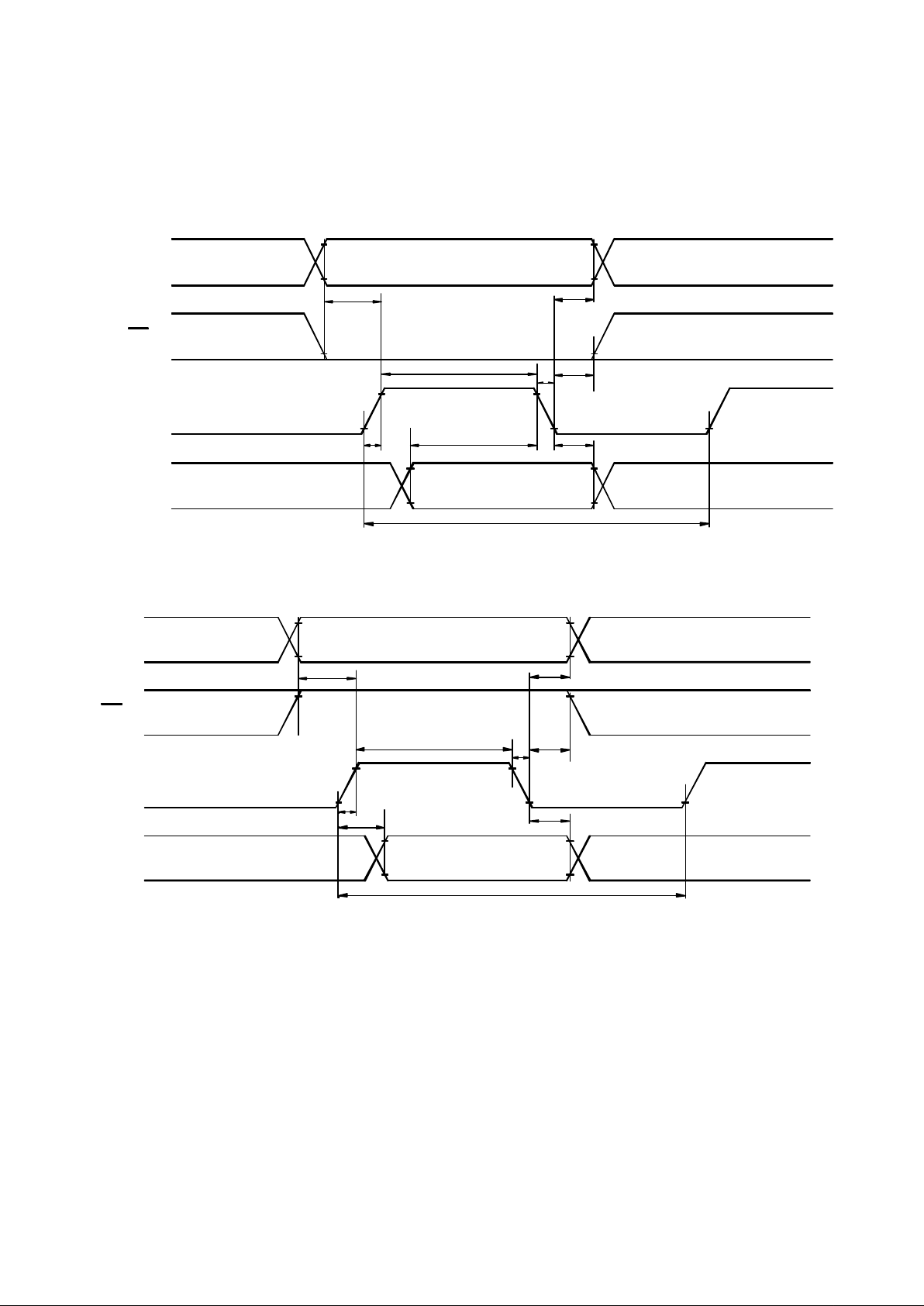
8.0 TIMING CHARACTERISTICS
Item Symbol Test Condition Min. Typ. Max. Unit
Enable cycle time t
C
Fig. a, Fig. b
500 - - ns
Enable pulse width t
W
Fig. a, Fig. b
220 - - ns
Enable rise/fall time t
R
, t
F
Fig. a, Fig. b
- - 25 ns
RS, R/W set up time t
SU
Fig. a, Fig. b
40 - - ns
RS, R/W hold time t
H
Fig. a, Fig. b
10 - - ns
Data delay time
t
D Fig. b
- - 120 ns
Data set up time t
DSU
Fig. a
60 - - ns
Data hold time t
DH
Fig. a, Fig. b
20 - - ns
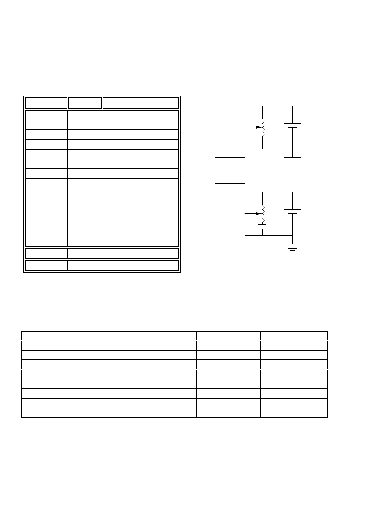
Vss
Vo
Vdd
Vr
+5V
STANDARD TEMP RANGE
Vss
Vo
Vdd
Vr
+5V
WIDE TEMP RANGE
-5V
Vr = 10K Ω ~ 20KΩ
Page 6
ACM2402F SERIES LCD MODULE
AZ DISPLAYS, INC. 11/20/00 6
VIH1
VIL1
VIL1
IH1
IL1
V
V
V
IH1
VIL1
V IL1
V
IH1
IL1V
V
IH1
IL1V
Valid Data
tSU
tH
t
W tH
t
F
tR
tDSU t
DH
tC
RS
R/W
E
DB0~DB7
V IL1
V IH1
VIL1
Fig. a Interface timing (data write)
V
IH1
V
IL1
V
IH1
IH1
IL1
V
V V
IH1
V
IL1
V
IH1
V
IH1
IL1
V
V
IH1
IL1
V
Valid Data
t
SU
t
H
t W
t
H
tF
t
R
t
DSU
t
DH
t
C
RS
R/W
E
DB0~DB7
V
IL1
t D
V
IH1
IL1
V
Fig. b Interface timing (data read)
Page 7
ACM2402F SERIES LCD MODULE
AZ DISPLAYS, INC. 11/20/00 7
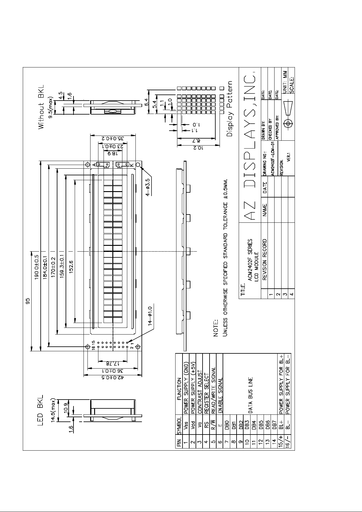
9.0 MECHANICAL DIAGRAM
Page 8
ACM2402F SERIES LCD MODULE
AZ DISPLAYS, INC. 11/20/00 8
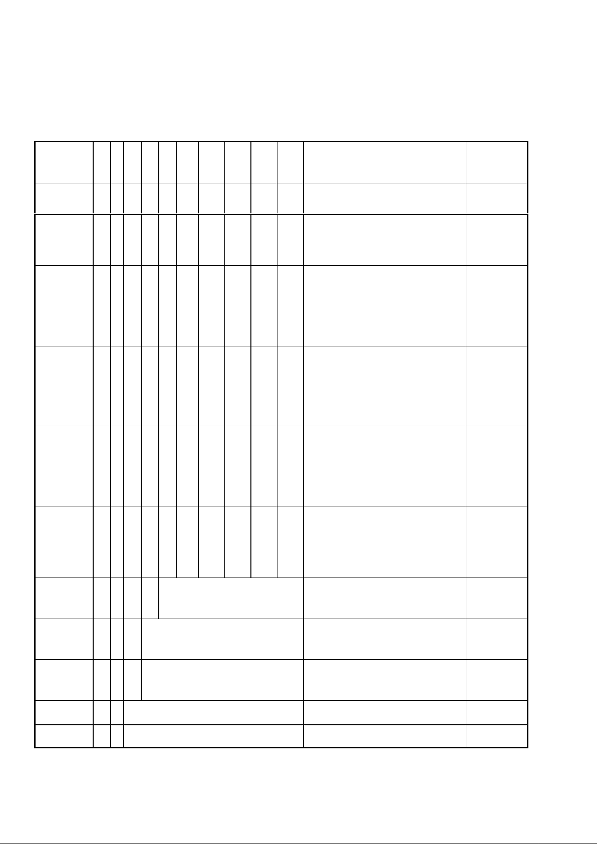
11.0 DISPLAY INSTRUCTION TABLE
COMMAND RSR/WDB7DB6DB5DB4DB3DB2DB1DB
0
DESCRIPTION Executing
time
fosc=250khz
Clear
Display
0 0 0 0 0 0 0 0 0 1 Clears Display & Returns to Address
0.
1.64ms
0 0 0 0 0 0 0 0 1 x Returns Cursor to Address 0. Also
returns the display being shifted to the
original position. DDRAM contents
remain unchanged.
1.64ms
0 0 0 0 0 0 0 1 I/D S I/D: Set Cursor Moving Direction
I/D=1: Increment
I/D=0: Decrement
S: Specify Shift of Display
S=1: The display is shifted
S=0: The display is not shifted
40µs
Display
ON/OFF
Control
0 0 0 0 0 0 1 D C B Display D=1: Display on
D=0: Display off
Cursor C=1: Cursor on
C=0: Cursor off
Brink B=1: Brink on
B=0: Brink off
40µs
Cursor /
Display
Shift
0
0
0 0 0 1 S/C R/L x x Moves cursor or shifts the display w/o
changing DD RAM contents
S/C=0: Cursor Shift (RAM unchanged)
S/C=1: Display Shift (RAM
unchanged)
R/L=1: Shift to the Right
R/L=0: Shift to the Left
40µs
Function
Set
0 0 0 0 1 DL N F x x Sets data bus length (DL), # of display
lines (N), and character fonts (F).
DL=1: 8 bits F=0: 5x7 dots
DL=0: 4 bits F=1: 5x10 dots
N=0: 1 line display
N=1: 2 lines display
40µs
Set CG
RAM
Address
0
0
0 1 Character Generator (CG) RAM
Address
Sets CG RAM address. CG RAM data
is sent and received after this
instruction.
40µs
Set DD
RAM
Address
0 0 1 Display Data (DD) RAM Address /
Cursor Address
Sets DD RAM address. DD Ram data
is sent and received after this
instruction.
40µs
Busy Flag /
Address
Read
0 1 BFAddress counter used for both DD &
CG RAM address
Reads Busy Flag (BF) and address
counter contents.
40µs
Write Data 1 0 Write Data Writes data into DDRAM or CGRAM. 46µs
Read Data
1
1
Read Data Reads data from DDRAM or CGRAM. 46µs
 Loading...