

Page 1

A28F400BX-T/B
4-MBIT (256K x16, 512K x8) BOOT BLOCK FLASH
MEMORY FAMILY
Automotive
Y
x8/x16 Input/Output Architecture
Ð A28F400BX-T, A28F400BX-B
Ð For High Performance and High
Integration 16-bit and 32-bit CPUs
Y
Optimized High Density Blocked
Architecture
Ð One 16 KB Protected Boot Block
Ð Two 8 KB Parameter Blocks
Ð One 96 KB Main Block
Ð Three 128 KB Main Blocks
Ð Top or Bottom Boot Locations
Y
Extended Cycling Capability
Ð 1,000 Block Erase Cycles
Y
Automated Word/Byte Write and Block
Erase
Ð Command User Interface
Ð Status Register
Ð Erase Suspend Capability
Y
SRAM-Compatible Write Interface
Y
Automatic Power Savings Feature
Ð 1 mA Typical I
Active Current in
CC
Static Operation
Y
Very High-Performance Read
Ð 90 ns Maximum Access Time
Ð 45 ns Maximum Output Enable Time
Y
Low Power Consumption
Ð 25 mA Typical Active Read Current
Y
Deep Power-Down/Reset Input
Ð Acts as Reset for Boot Operations
Y
Automotive Temperature Operation
b
Ð
40§Ctoa125§C
Y
Write Protection for Boot Block
Y
Hardware Data Protection Feature
Ð Erase/Write Lockout During Power
Transitions
Y
Industry Standard Surface Mount
Packaging
Ð JEDEC ROM Compatible
44-Lead PSOP
Y
12V Word/Byte Write and Block Erase
e
ÐV
Y
ETOXTMIII Flash Technology
12Vg5% Standard
PP
Ð 5V Read
*Other brands and names are the property of their respective owners.
Information in this document is provided in connection with Intel products. Intel assumes no liability whatsoever, including infringement of any patent or
copyright, for sale and use of Intel products except as provided in Intel’s Terms and Conditions of Sale for such products. Intel retains the right to make
changes to these specifications at any time, without notice. Microcomputer Products may have minor variations to this specification known as errata.
November 1995COPYRIGHT©INTEL CORPORATION, 1995 Order Number: 290501-003
Page 2

A28F400BX-T/B
Intel’s 4-Mbit Flash Memory Family is an extension of the Boot Block Architecture which includes blockselective erasure, automated write and erase operations and standard microprocessor interface. The 4-Mbit
Flash Memory Family enhances the Boot Block Architecture by adding more density and blocks, x8/x16 input/
output control, very high speed, low power, an industry standard ROM compatible pinout and surface mount
packaging. The 4-Mbit flash family is an easy upgrade from Intel’s 2-Mbit Boot Block Flash Memory Family.
The Intel A28F400BX-T/B are 16-bit wide flash memory offerings optimized to meet the rigorous environmental requirements of Automotive Applications. These high density flash memories provide user selectable bus
operation for either 8-bit or 16-bit applications. The A28F400BX-T and A28F400BX-B are 4,194,304-bit nonvolatile memories organized as either 524,288 bytes or 262,144 words of information. They are offered in 44Lead plastic SOP packages. The x8/x16 pinout conforms to the industry standard ROM/EPROM pinout. Read
and Write characteristics are guaranteed over the ambient temperature range of
These devices use an integrated Command User Interface (CUI) and Write State Machine (WSM) for simplified
word/byte write and block erasure. The A28F400BX-T provide block locations compatible with Intel’s
MCS-186 family, 80286, i386
TM
, i486TM, i860TMand 80960CA microprocessors. The A28F400BX-B provides
compatibility with Intel’s 80960KX and 80960SX families as well as other embedded microprocessors.
The boot block includes a data protection feature to protect the boot code in critical applications. With a
maximum access time of 90 ns, these 4-Mbit flash devices are very high performance memories which
interface at zero-wait-state to a wide range of microprocessors and microcontrollers.
Manufactured on Intel’s 0.8 micron ETOX
TM
III process, the 4-Mbit flash memory family provides world class
quality, reliability and cost-effectiveness at the 4-Mbit density level.
b
40§Ctoa125§C.
2
Page 3

A28F400BX-T/B
1.0 PRODUCT FAMILY OVERVIEW
Throughout this datasheet the A28F400BX refers to
both the A28F400BX-T and A28F400BX-B devices.
Section 1 provides an overview of the 4-Mbit flash
memory family including applications, pinouts and
pin descriptions. Section 2 describes in detail the
specific memory organization for the A28F400BX.
Section 3 provides a description of the family’s principles of operations. Finally the family’s operating
specifications are described.
1.1 Main Features
The A28F400BX boot block flash memory family is a
very high performance 4-Mbit (4,194,304 bit) memory family organized as either 256-KWords (262,144
words) of 16 bits each or 512-Kbytes (524,288
bytes) of 8 bits each.
Seven Separately Erasable Blocks including a
Hardware-Lockable boot block (16,384 Bytes),
Two parameter blocks (8,192 Bytes each) and
Four main blocks (1 block of 98,304 Bytes and 3
blocks of 131,072 Bytes) are included on the 4-Mbit
family. An erase operation erases one of the main
blocks in typically 3 seconds and the boot or parameter blocks in typically 1.5 seconds independent of
the remaining blocks. Each block can be independently erased and programmed 1,000 times.
The Boot Block is located at either the top
(A28F400BX-T) or the bottom (A28F400BX-B) of the
address map in order to accommodate different microprocessor protocols for boot code location. The
hardware lockable boot block provides the most
secure code storage. The boot block is intended to
store the kernel code required for booting-up a system. When the RP
the boot block is unlocked and program and erase
operations can be performed. When the RP
at or below 6.5V the boot block is locked and program and erase operations to the boot block are
ignored.
The A28F400BX products are available in the ROM/
EPROM compatible pinout and housed in the
44-Lead PSOP (Plastic Small Outline) package as
shown in Figure 3.
The Command User Interface (CUI) serves as the
interface between the microprocessor or microcontroller and the internal operation of the A28F400BX
flash memory.
Program and Erase Automation allows program
and erase operations to be executed using a twowrite command sequence to the CUI. The internal
Write State Machine (WSM) automatically executes
Ý
pin is between 11.4V and 12.6V
Ý
pin is
the algorithms and timings necessary for program
and erase operations, including verifications, thereby unburdening the microprocessor or microcontroller. Writing of memory data is performed in word or
byte increments typically within 9 ms which is a
100% improvement over previous flash memory
products.
The Status Register (SR) indicates the status of the
WSM and whether the WSM successfully completed
the desired program or erase operation.
Maximum Access Time of 90 ns (TACC) is achieved
over the automotive temperature range, 10% V
supply range (4.5V to 5.5V) and 100 pF output load.
maximum Program current is 40 mA for x16
I
PP
operation and 30 mA for x8 operation. I
current is 30 mA maximum. V
gramming voltage is 11.4V to 12.6V (V
g
5%) under all operating conditions. Typical
Active Current of 25 mA is achieved.
I
CC
erase and pro-
PP
PP
PP
Erase
e
CC
12V
The 4-Mbit boot block flash memory family is also
designed with an Automatic Power Savings (APS)
feature to minimize system battery current drain and
allows for very low power designs. Once the device
is accessed to read array data, APS mode will immediately put the memory in static mode of operation
where I
next read is initiated.
When the CE
BYTE
Standby mode is enabled where I
80 mA.
active current is typically 1 mA until the
CC
Ý
Ý
and RPÝpins are at VCCand the
pin is at either VCCor GND the CMOS
is typically
CC
A Deep Power-Down Mode is enabled when the
Ý
RP
pin is at ground minimizing power consumption
and providing write protection during power-up conditions. I
is 50 mA typical. An initial maximum access time or
Reset Time of 300 ns is required from RP
current during deep power-down mode
CC
Ý
switching until outputs are valid. Equivalently, the device
has a maximum wake-up time of 210 ns until writes
to the Command User Interface are recognized.
When RP
Ý
is at ground the WSM is reset, the
Status Register is cleared and the entire device is
protected from being written to. This feature prevents data corruption and protects the code stored
in the device during system reset. The system Reset
Ý
pin can be tied to RP
to reset the memory to normal read mode upon activation of the Reset pin.
With on-chip program/erase automation in the
4-Mbit family and the RP
Ý
functionality for data protection, when the CPU is reset and even if a program
or erase command is issued, the device will not recognize any operation until RP
Ý
returns to its normal
state.
3
Page 4

A28F400BX-T/B
For the A28F400BX, Byte-wide or Word-wide Input/Output Control is possible by controlling the
Ý
BYTE
the device is in the byte-wide mode (x8) and data is
read and written through DQ[0:7]. During the bytewide mode, DQ[8:14]are tri-stated and DQ15/A-1
becomes the lowest order address pin. When the
BYTE
word-wide mode (x16) and data is read and written
through DQ[0:15].
pin. When the BYTEÝpin is at a logic low
Ý
pin is at a logic high the device is in the
1.2 Applications
The 4-Mbit boot block flash memory family combines high density, high performance, cost-effective
flash memories with blocking and hardware protec-
tion capabilities. Its flexibility and versatility will reduce costs throughout the product life cycle. Flash
memory is ideal for Just-In-Time production flow, reducing system inventory and costs, and eliminating
component handling during the production phase.
During the product life cycle, when code updates or
feature enhancements become necessary, flash
memory will reduce the update costs by allowing either a user-performed code change via floppy disk
or a remote code change via a serial link. The 4-Mbit
boot block flash memory family provides full function, blocked flash memories suitable for a wide
range of automotive applications.
4
Page 5
A28F400BX-T/B
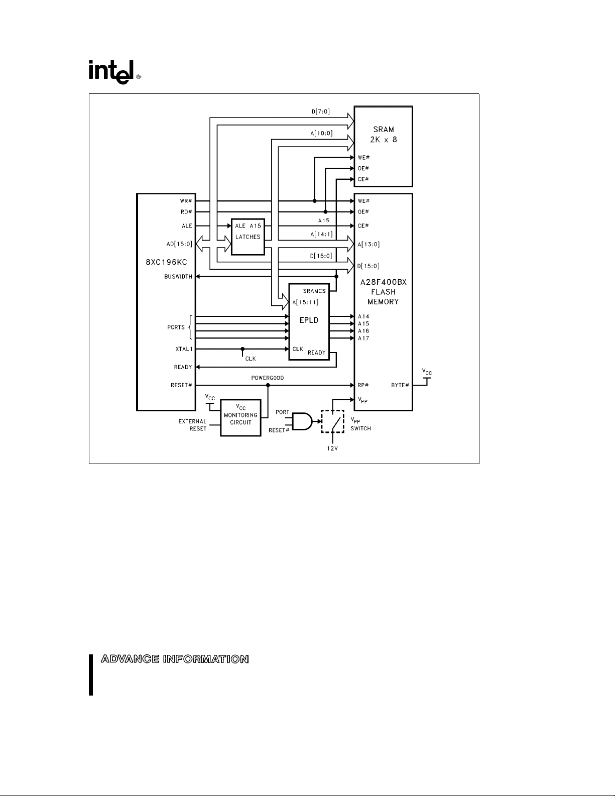
Figure 1. A28F400BX Interface to 8XC196KC
290501– 1
5
Page 6
A28F400BX-T/B
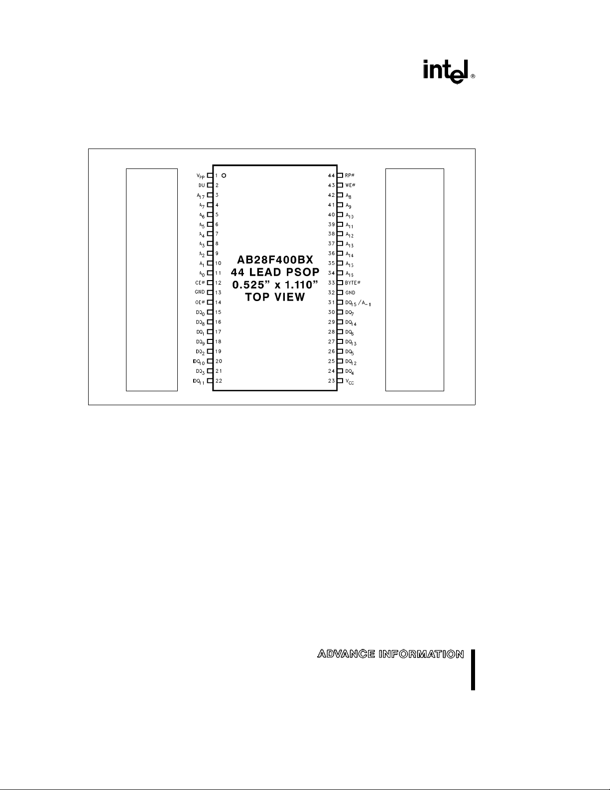
1.3 Pinouts
The A28F400BX 44-Lead PSOP pinout follows the
industry standard ROM/EPROM pinout as shown in
Figure 2.
27C400
NC
NC
A
17
A
7
A
6
A
5
A
4
A
3
A
2
A
1
A
0
Ý
CE
GND
Ý
OE
DQ
0
DQ
8
DQ
1
DQ
9
DQ
2
DQ
10
DQ
3
DQ
11
290501– 3
Figure 2. PSOP Lead Configuration
27C400
NC
NC
A
8
A
9
A
10
A
11
A
12
A
13
A
14
A
15
A
16
BYTEÝ/V
GND
DQ
/A
15
DQ
7
DQ
14
DQ
6
DQ
13
DQ
5
DQ
12
DQ
4
V
CC
PP
b
1
6
Page 7
A28F400BX-T/B
1.4 A28F400BX Pin Descriptions
Symbol Type Name and Function
A0–A
17
A
9
DQ0–DQ7I/O DATA INPUTS/OUTPUTS: Inputs array data on the second CEÝand WEÝcycle during a
DQ8–DQ15I/O DATA INPUTS/OUTPUTS: Inputs array data on the second CEÝand WEÝcycle during a
Ý
CE
Ý
RP
Ý
OE
Ý
WE
Ý
BYTE
V
PP
V
CC
GND GROUND: For all internal circuitry.
NC NO CONNECT: Pin may be driven or left floating.
DU DON’T USE PIN: Pin should not be connected to anything.
I ADDRESS INPUTS for memory addresses. Addresses are internally latched during a write
cycle.
I ADDRESS INPUT: When A9is at 12V the signature mode is accessed. During this mode A
decodes between the manufacturer and device ID’s. When BYTEÝis at a logic low only the
lower byte of the signatures are read. DQ
Ý
is low.
BYTE
program command. Inputs commands to the command user interface when CE
/A
is a don’t care in the signature mode when
b
15
1
Ý
and WE
are active. Data is internally latched during the write and program cycles. Outputs array,
intelligent identifier and Status Register data. The data pins float to tri-state when the chip is
deselected or the outputs are disabled.
program command. Data is internally latched during the write and program cycles. Outputs
array data. The data pins float to tri-state when the chip is deselected or the outputs are
disabled as in the byte-wide mode (BYTE
becomes the lowest order address for data output on DQ0-DQ7.
e
Ý
‘‘0’’). In the byte-wide mode DQ15/A
b
1
I CHIP ENABLE: Activates the device’s control logic, input buffers, decoders and sense
amplifiers. CE
consumption to standby levels. If CE
standby current will increase due to current flow through the CE
Ý
is active low; CEÝhigh deselects the memory device and reduces power
Ý
and RPÝare high, but not at a CMOS high level, the
Ý
and RPÝinput stages.
I RESET/POWER-DOWN: Provides three-state control. Puts the device in deep power-down
mode. Locks the boot block from program/erase.
Ý
When RP
is at logic high level and equals 6.5V maximum the boot block is locked and
cannot be programmed or erased.
e
Ý
When RP
11.4V minimum the boot block is unlocked and can be programmed or
erased.
Ý
When RP
is at a logic low level the boot block is locked, the deep power-down mode is
enabled and the WSM is reset preventing any blocks from being programmed or erased,
Ý
therefore providing data protection during power transitions. When RP
transitions from
logic low to logic high the flash memory enters the read array mode.
I OUTPUT ENABLE: Gates the device’s outputs through the data buffers during a read cycle.
Ý
OE
is active low.
I WRITE ENABLE: Controls writes to the Command Register and array blocks. WEÝis active
Ý
low. Addresses and data are latched on the rising edge of the WE
pulse.
I BYTEÝENABLE: Controls whether the device operates in the byte-wide mode (x8) or the
Ý
word-wide mode (x16). BYTE
CMOS current in the standby mode. BYTE
is read and programmed on DQ
that decodes between the upper and lower byte. DQ
wide mode. BYTE
programmed on DQ
Ý
0
e
–DQ15.
pin must be controlled at CMOS levels to meet 130 mA
–DQ7and DQ15/A
0
‘‘1’’ enables the word-wide mode where data is read and
e
Ý
‘‘0’’ enables the byte-wide mode, where data
becomes the lowest order address
b
1
–DQ14are tri-stated during the byte-
8
PROGRAM/ERASE POWER SUPPLY: For erasing memory array blocks or programming
data in each block.
Note: V
k
V
PP
memory contents cannot be altered.
PPLMAX
DEVICE POWER SUPPLY (5Vg10%)
0
Ý
7
Page 8
A28F400BX-T/B
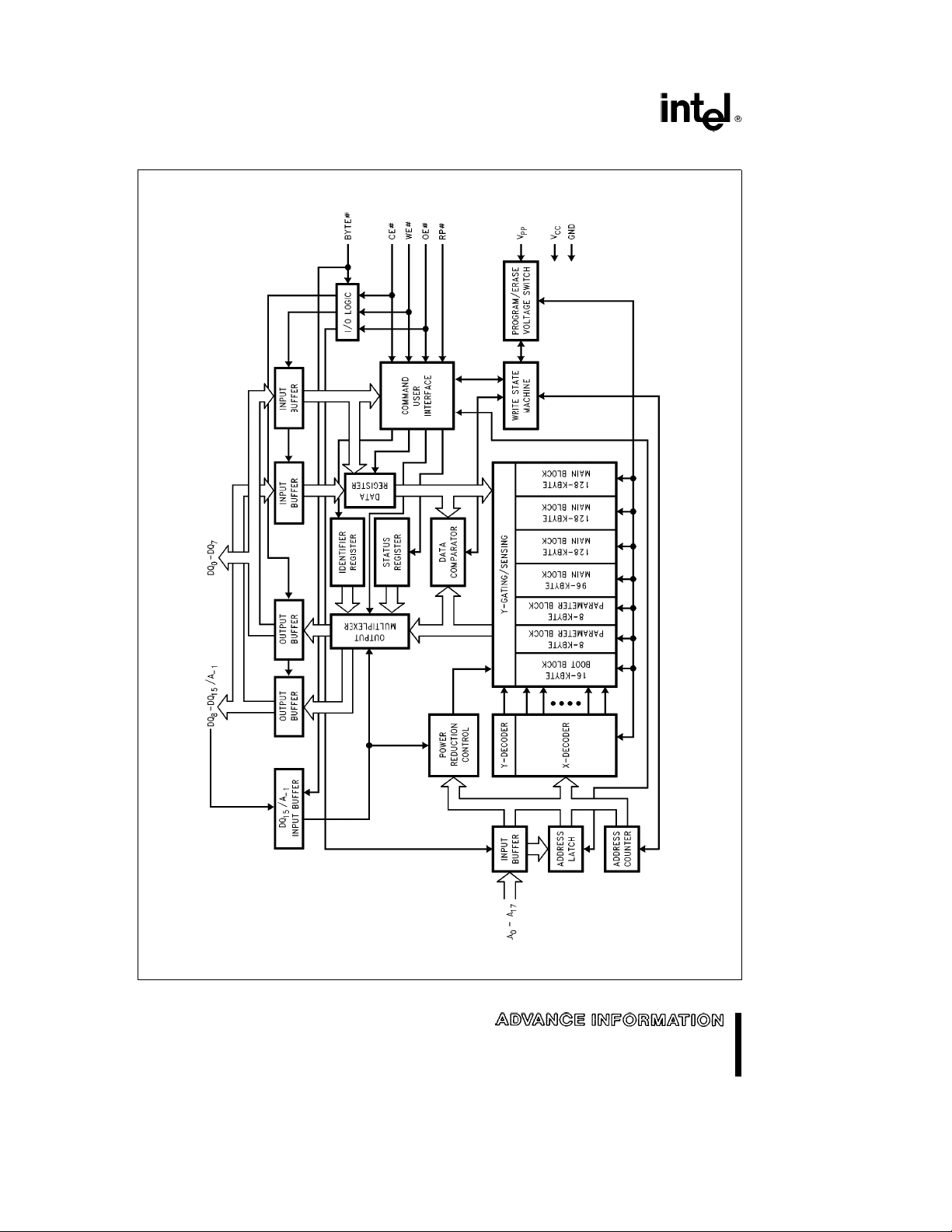
2.0 A28F400BX WORD/BYTE-WIDE PRODUCTS DESCRIPTION
290501– 4
Figure 3. A28F400BX Word/Byte Block Diagram
8
Page 9
A28F400BX-T/B
2.1 A28F400BX Memory Organization
2.1.1 BLOCKING
The A28F400BX uses a blocked array architecture
to provide independent erasure of memory blocks. A
block is erased independently of other blocks in the
array when an address is given within the block address range and the Erase Setup and Erase Confirm
commands are written to the CUI. The A28F400BX
is a random read/write memory, only erasure is performed by block.
2.1.1.1 Boot Block Operation and Data
Protection
The 16-Kbyte boot block provides a lock feature for
secure code storage. The intent of the boot block is
to provide a secure storage area for the kernel code
that is required to boot a system in the event of power failure or other disruption during code update.
This lock feature ensures absolute data integrity by
preventing the boot block from being written or
erased when RP
be erased and written when RP
the duration of the erase or program operation. This
allows customers to change the boot code when
necessary while providing security when needed.
See the Block Memory Map section for address locations of the boot block for the A28F400BX-T and
A28F400BX-B.
2.1.1.2 Parameter Block Operation
The A28F400BX has 2 parameter blocks (8 Kbytes
each). The parameter blocks are intended to provide
storage for frequently updated system parameters
and configuration or diagnostic information. The parameter blocks can also be used to store additional
boot or main code. The parameter blocks however,
do not have the hardware write protection feature
that the boot block has. The parameter blocks provide for more efficient memory utilization when dealing with parameter changes versus regularly blocked
devices. See the Block Memory Map section for address locations of the parameter blocks for the
A28F400BX-T and A28F400BX-B.
2.1.1.3 Main Block Operation
Four main blocks of memory exist on the
A28F400BX (3 x 128 Kbyte blocks and 1 x 96-Kbyte
blocks). See the following section on Block Memory
Map for the address location of these blocks for the
A28F400BX-T and A28F400BX-B products.
Ý
is not at 12V. The boot block can
Ý
is held at 12V for
2.1.2 BLOCK MEMORY MAP
Two versions of the A28F400BX product exist to
support two different memory maps of the array
blocks in order to accommodate different microprocessor protocols for boot code location. The
A28F400BX-T memory map is inverted from the
A28F400BX-B memory map.
2.1.2.1. A28F400BX-B Memory Map
The A28F400BX-B device has the 16-Kbyte boot
block located from 00000H to 01FFFH to accommodate those microprocessors that boot from the bottom of the address map at 00000H. In the
A28F400BX-B the first 8-Kbyte parameter block resides in memory space from 02000H to 02FFFH.
The second 8-Kbyte parameter block resides in
memory space from 03000H to 03FFFH. The 96Kbyte main block resides in memory space from
04000H to 0FFFFH. The three 128-Kbyte main
block resides in memory space from 10000H to
1FFFFH, 20000H to 2FFFFH and 30000H to
3FFFFH (word locations). See Figure 4.
(Word Addresses)
3FFFFH
128-Kbyte MAIN BLOCK
30000H
2FFFFH
128-Kbyte MAIN BLOCK
20000H
1FFFFH
128-Kbyte MAIN BLOCK
10000H
0FFFFH
96-Kbyte MAIN BLOCK
04000H
03FFFH
03000H
02FFFH
02000H
01FFFH
00000H
8-Kbyte PARAMETER BLOCK
8-Kbyte PARAMETER BLOCK
16-Kbyte BOOT BLOCK
Figure 4. A28F400BX-B Memory Map
9
Page 10
A28F400BX-T/B
2.1.2.2 A28F400BX-T Memory Map
The A28F400BX-T device has the 16-Kbyte boot
block located from 3E000H to 3FFFFH to accommodate those microprocessors that boot from the top
of the address map. In the A28F400BX-T the first
8-Kbyte parameter block resides in memory space
from 3D000H to 3DFFFH. The second 8-Kbyte parameter block resides in memory space from
3C000H to 3CFFFH. The 96-Kbyte main block resides in memory space from 30000H to 3BFFFH.
The three 128-Kbyte main blocks reside in memory
space from 20000H to 2FFFFH, 10000H to 1FFFFH
and 00000H to 0FFFFH as shown below in Figure 5.
(Word Addresses)
3FFFFH
3E000H
3DFFFH
3D000H
3CFFFH
3C000H
3BFFFH
30000H
2FFFFH
20000H
1FFFFH
10000H
0FFFFH
16-Kbyte BOOT BLOCK
8-Kbyte PARAMETER BLOCK
8-Kbyte PARAMETER BLOCK
96-Kbyte MAIN BLOCK
128-Kbyte MAIN BLOCK
128-Kbyte MAIN BLOCK
128-Kbyte MAIN BLOCK
3.0 PRODUCT FAMILY PRINCIPLES
OF OPERATION
Flash memory augments EPROM functionality with
in-circuit electrical write and erase. The 4-Mbit flash
family utilizes a Command User Interface (CUI) and
internally generated and timed algorithms to simplify
write and erase operations.
The CUI allows for 100% TTL-level control inputs,
fixed power supplies during erasure and programming, and maximum EPROM compatibility.
In the absence of high voltage on the V
4-Mbit boot block flash family will only successfully
execute the following commands: Read Array, Read
Status Register, Clear Status Register and Intelligent Identifier mode. The device provides standard
EPROM read, standby and output disable operations. Manufacturer Identification and Device Identification data can be accessed through the CUI or
through the standard EPROM A
cess (V
) for PROM programming equipment.
ID
high voltage ac-
9
The same EPROM read, standby and output disable
functions are available when high voltage is applied
to the V
lows write and erase of the device. All functions as-
pin. In addition, high voltage on VPPal-
PP
sociated with altering memory contents: write and
erase, Intelligent Identifier read and Read Status are
accessed via the CUI.
The purpose of the Write State Machine (WSM) is to
completely automate the write and erasure of the
device. The WSM will begin operation upon receipt
of a signal from the CUI and will report status back
through a Status Register. The CUI will handle the
Ý
WE
interface to the data and address latches, as
well as system software requests for status while the
WSM is in operation.
PP
pin, the
00000H
Figure 5. A28F400BX-T Memory Map
10
3.1 Bus Operations
Flash memory reads, erases and writes in-system
via the local CPU. All bus cycles to or from the flash
memory conform to standard microprocessor bus
cycles.
Page 11
A28F400BX-T/B
e
Table 1. Bus Operations for WORD-WIDE Mode (BYTE
Mode Notes RPÝCEÝOEÝWE
Read 1, 2, 3 V
Output Disable V
Standby V
Deep Power-Down 9 V
Intelligent Identifier (Mfr) 4 V
Intelligent Identifier (Device) 4, 5 V
Write 6, 7, 8 V
V
IH
V
IH
V
IH
IL
V
IH
V
IH
V
IH
V
IL
IL
IH
IL
V
IH
X X X X X High Z
X X X X X X High Z
V
IL
IL
IL
IL
V
IL
V
IH
Table 2. Bus Operations for BYTE-WIDE Mode (BYTEeVIL)
Mode Notes RPÝCEÝOEÝWEÝA9A0A
Read 1, 2, 3 V
Output Disable V
Standby V
Deep Power-Down 9 V
Intelligent 4 V
V
V
V
IH
IL
IL
V
IH
IH
IL
IH
V
IL
IH
V
X X X X X X High Z High Z
IH
X X X X X X X High Z High Z
V
V
IL
IL
XX X XD
IH
V
X X X X High Z High Z
IH
V
IHVIDVIL
Identifier (Mfr)
Intelligent 4, 5 V
V
V
IH
IL
IL
V
IHVIDVIH
Identifier (Device) 71H
Write 6, 7, 8 V
NOTES:
1. Refer to DC Characteristics.
2. X can be V
3. See DC Characteristics for V
4. Manufacturer and Device codes may also be accessed via a CUI write sequence. A
5. Device ID
6. Refer to Table 3 for valid D
7. Command writes for Block Erase or Word/Byte Write are only executed when V
8. To write or erase the boot block, hold RP
Ý
must be at GNDg0.2V to meet the 80 mA maximum deep power-down current.
9. RP
for control pins and addresses, V
IL,VIH
e
4470H for A28F400BX-T and 4471H for A28F400BX-B.
PPL,VPPH,VHH,VID
during a write operation.
IN
V
V
V
IH
IL
IH
or V
PPL
PPH
Ý
voltages.
at VHH.
XX X X DINHigh Z
IL
for VPP.
Ý
VIH)
Ý
A9A0V
V
V
V
V
V
XX X D
IH
X X X High Z
IH
VIDV
IH
IH
IL
b
IL
VIDV
IH
XX X D
1VPP
X X 89H High Z
X X 70H High Z
e
X.
V
.
PPH
PP
1–A17
e
DQ
DQ
PP
0–15
OUT
X 0089H
X 4470H
4471H
IN
DQ
0–7
OUT
8–14
High Z
3.2 Read Operations
The 4-Mbit boot block flash family has three user
read modes; Array, Intelligent Identifier, and Status
Register. Status Register read mode will be discussed in detail in the ‘‘Write Operations’’ section.
During power-up conditions (V
takes a maximum of 300 ns from when V
4.5V minimum to valid data on the outputs.
supply ramping), it
CC
CC
is at
3.2.1 READ ARRAY
If the memory is not in the Read Array mode, it is
necessary to write the appropriate read mode command to the CUI. The 4-Mbit boot block flash family
has three control functions, all of which must be logically active, to obtain data at the outputs. Chip-En-
Ý
able CE
Power-Down, RP
put-Enable OE
is the device selection control. Reset/
Ý
is the device power control. Out-
Ý
is the DATA INPUT/OUTPUT
(DQ[0:15]or DQ[0:7]) direction control and when
active is used to drive data from the selected memory on to the I/O bus.
11
Page 12

A28F400BX-T/B
3.2.1.1 Output Control
With OEÝat logic-high level (VIH), the output from
the device is disabled and data input/output pins
(DQ[0:15]or DQ[0:7]are tri-stated. Data input is
then controlled by WE
Ý
.
3.2.1.2 Input Control
With WE
Ý
at logic-high level (VIH), input to the device is disabled. Data Input/Output pins (DQ[0:15
or DQ[0:7]) are controlled by OE
Ý
.
3.2.2 INTELLIGENT IDENTIFIERS
The manufacturer and device codes are read via the
CUI or by taking the A
the CUI places the device into Intelligent Identifier
pin to 12V. Writing 90H to
9
read mode. A read of location 00000H outputs the
manufacturer’s identification code, 0089H, and location 00001H outputs the device code; 4470H for
A28F400BX-T, 4471H for A28F400BX-B. When
Ý
BYTE
above signatures is read and DQ
care’’ during Intelligent Identifier mode. A read array
is at a logic low only the lower byte of the
/A
is a ‘‘don’t
b
15
1
command must be written to the memory to return to
the read array mode.
3.3 Write Operations
Commands are written to the CUI using standard microprocessor write timings. The CUI serves as the
interface between the microprocessor and the internal chip operation. The CUI can decipher Read Array, Read Intelligent Identifier, Read Status Register,
Clear Status Register, Erase and Program commands. In the event of a read command, the CUI
simply points the read path at either the array, the
Intelligent Identifier, or the status register depending
on the specific read command given. For a program
or erase cycle, the CUI informs the write state machine that a write or erase has been requested. During a program cycle, the Write State Machine will
control the program sequences and the CUI will only
respond to status reads. Durlng an erase cycle, the
CUI will respond to status reads and erase suspend.
After the Write State Machine has completed its
task, it will allow the CUI to respond to its full command set. The CUI will stay in the current command
state until the microprocessor issues another command.
The CUI will successfully initiate an erase or write
operation only when V
Depending upon the application, the system designer may choose to make the V
switchable, available only when memory updates
is within its voltage range.
PP
power supply
PP
are desired. The system designer can also choose
to ‘‘hard-wire’’ V
flash family is designed to accommodateÐeither de-
to 12V. The 4-Mbit boot block
PP
sign practice. It is strongly recommended that RP
be tied to logical Reset for data protection during
unstable CPU reset function as described in the
‘‘Product Family Overview’’ section.
3.3.1 BOOT BLOCK WRITE OPERATIONS
]
In the case of Boot Block modifications (write and
erase), RP
tion to V
However, if RP
Ý
is set to V
at high voltage.
PP
Ý
is not at VHHwhen a program or
e
12V typically, in addi-
HH
erase operation of the boot block is attempted, the
corresponding status register bit (Bit 4 for Program
and Bit 5 for Erase, refer to Table 5 for Status Register Definitions) is set to indicate the failure to complete the operation.
3.3.2 COMMAND USER INTERFACE (CUI)
The Command User Interface (CUI) serves as the
interface to the microprocessor. The CUI points the
read/write path to the appropriate circuit block as
described in the previous section. After the WSM
has completed its task, it will set the WSM Status bit
to a ‘‘1’’, which will also allow the CUI to respond to
its full command set. Note that after the WSM has
returned control to the CUI, the CUI will remain in its
current state.
3.3.2.1 Command Set
Command
Codes
Device Mode
00 Invalid/Reserved
10 Alternate Program Setup
20 Erase Setup
40 Program Setup
50 Clear Status Register
70 Read Status Register
90 Intelligent Identifier
B0 Erase Suspend
D0 Erase Resume/Erase Confirm
FF Read Array
3.3.2.2 Command Function Descriptions
Device operations are selected by writing specific
commands into the CUI. Table 3 defines the 4-Mbit
boot block flash family commands.
Ý
12
Page 13

A28F400BX-T/B
Table 3. Command Definitions
Bus
Command Cycles
Read Array 1 1 Write X FFH
Intelligent Identifier 3 2, 4 Write X 90H Read IA IID
Read Status Register 2 3 Write X 70H Read X SRD
Clear Status Register 1 Write X 50H
Erase Setup/Erase Confirm 2 5 Write BA 20H Write BA D0H
Word/Byte Write Setup/Write 2 6, 7 Write WA 40H Write WA WD
Erase Suspend/Erase Resume 2 Write X B0H Write X D0H
Alternate Word/Byte 2 6, 7 Write WA 10H Write WA WD
Write Setup/Write
NOTES:
1. Bus operations are defined in Tables 1, and 2.
e
Identifier Address: 00H for manufacturer code, 01H for device code.
2. IA
e
3. SRD
4. IID
Following the Intelligent Identifier Command, two read operations access manufacturer and device codes.
5. BA
6. WA
WD
7. Either 40H or 10H commands is valid.
8. When writing commands to the device, the upper data bus[DQ
additional current.
Data read from Status Register.
e
Intelligent Identifier Data.
e
Address within the block being erased.
e
Address to be written.
e
Data to be written at location WD.
Notes First Bus Cycle Second Bus Cycle
Req’d
8 Operation Address Data Operation Address Data
e
]
8
–DQ
X which is either VCCor VSSto avoid burning
15
Invalid/Reserved
These are unassigned commands. It is not recommended that the customer use any command other
than the valid commands specified above. Intel reserves the right to redefine these codes for future
functions.
Read Array (FFH)
This single write command points the read path at
the array. If the host CPU performs a CE
Ý
/OE
controlled read immediately following a two-write sequence that started the WSM, then the device will
output status register contents. If the Read Array
command is given after Erase Setup the device is
reset to read the array. A two Read Array command
sequence (FFH) is required to reset to Read Array
after Program Setup.
Intelligent Identifier (90H)
After this command is executed, the CUI points the
output path to the Intelligent Identifier circuits. Only
Intelligent Identifier values at addresses 0 and 1 can
be read (only address A
other address inputs are ignored).
is used in this mode, all
0
Read Status Register (70H)
This is one of the two commands that is executable
while the state machine is operating. After this command is written, a read of the device will output the
contents of the status register, regardless of the address presented to the device.
The device automatically enters this mode after program or erase has completed.
Ý
Clear Status Register (50H)
The WSM can only set the Program Status and
Erase Status bits in the status register, it can not
clear them. Two reasons exist for operating the
status register in this fashion. The first is a synchronization. The WSM does not know when the host
CPU has read the status register, therefore it would
not know when to clear the status bits. Secondly, if
the CPU is programming a string of bytes, it may be
more efficient to query the status register after programming the string. Thus, if any errors exist while
programming the string, the status register will return
the accumulated error status.
13
Page 14

A28F400BX-T/B
Program Setup (40H or 10H)
This command simply sets the CUI into a state such
that the next write will load the address and data
registers. Either 40H or 10H can be used for Program Setup. Both commands are included to accommodate efforts to achieve an industry standard
command code set.
Program
The second write after the program setup command,
will latch addresses and data. Also, the CUI initiates
the WSM to begin execution of the program algorithm. While the WSM finishes the algorithm, the device will output Status Register contents. Note that
the WSM cannot be suspended during programming.
Erase Setup (20H)
Prepares the CUI for the Erase Confirm command.
No other action is taken. If the next command is not
an Erase Confirm command then the CUI will set
both the Program Status and Erase Status bits of the
Status Register to a ‘‘1’’, place the device into the
Read Status Register state, and wait for another
command.
Erase Confirm (D0H)
If the previous command was an Erase Setup command, then the CUI will enable the WSM to erase, at
the same time closing the address and data latches,
and respond only to the Read Status Register and
Erase Suspend commands. While the WSM is executing, the device will output Status Register data
when OE
only be updated by toggling either OE
Erase Suspend (B0H)
This command only has meaning while the WSM is
executing an Erase operation, and therefore will only
be responded to during an erase operation. After
this command has been executed, the CUI will set
an output that directs the WSM to suspend Erase
operations, and then return to responding to only
Read Status Register or to the Erase Resume commands. Once the WSM has reached the Suspend
state, it will set an output into the CUI which allows
the CUI to respond to the Read Array, Read Status
Register, and Erase Resume commands. In this
mode, the CUI will not respond to any other commands. The WSM will also set the WSM Status bit to
a ‘‘1’’. The WSM will continue to run, idling in the
SUSPEND state, regardless of the state of all input
Ý
is toggled low. Status Register data can
Ý
or CEÝlow.
Ý
control pins, with the exclusion of RP
.RPÝwill
immediately shut down the WSM and the remainder
of the chip. During a suspend operation, the data
and address latches will remain closed, but the address pads are able to drive the address into the
read path.
Erase Resume (D0H)
This command will cause the CUI to clear the Suspend state and set the WSM Status bit to a ‘‘0’’, but
only if an Erase Suspend command was previously
issued. Erase Resume will not have any effect in all
other conditions.
3.3.3 STATUS REGISTER
The 4-Mbit boot block flash family contains a status
register which may be read to determine when a program or erase operation is complete, and whether
that operation completed successfully. The status
register may be read at any time by writing the Read
Status command to the CUI. After writing this command, all subsequent Read operations output data
from the status register until another command is
written to the CUI. A Read Array command must be
written to the CUI to return to the Read Array mode.
The status register bits are output on DQ[0:7
whether the device is in the byte-wide (x8) or wordwide (x16) mode. In the word-wide mode the upper
byte, DQ[8:15]is set to 00H during a Read Status
command. In the byte-wide mode, DQ[8:14]are tristated and DQ
function.
/A
retains the low order address
b
15
1
It should be noted that the contents of the status
register are latched on the falling edge of OEÝor
Ý
CE
whichever occurs last in the read cycle. This
prevents possible bus errors which might occur if the
contents of the status register change while reading
the status register. CE
Ý
or OEÝmust be toggled
with each subsequent status read, or the completion
of a program or erase operation will not be evident.
The Status Register is the interface between the microprocessor and the Write State Machine (WSM).
When the WSM is active, this register will indicate
the status of the WSM, and will also hold the bits
indicating whether or not the WSM was successful in
performing the desired operation. The WSM sets
status bits ‘‘Three’’ through ‘‘Seven’’ and clears bits
‘‘Six’’ and ‘‘Seven’’, but cannot clear status bits
‘‘Three’’ through ‘‘Five’’. These bits can only be
cleared by the controlling CPU through the use of
the Clear Status Register command.
]
14
Page 15

3.3.3.1 Status Register Bit Definition
Table 4. Status Register Definitions
WSMS ESS ES PS VPPS R R R
76543210
e
SR.7
WRITE STATE MACHINE STATUS
e
Ready
1
e
Busy
0
e
ERASE SUSPEND STATUS
SR.6
e
Erase Suspended
1
e
Erase in Progress/Completed
0
e
ERASE STATUS
SR.5
e
Error in Block Erasure
1
e
Successful Block Erase
0
e
PROGRAM STATUS
SR.4
e
Error In Byte/Word Program
1
e
Successful Byte/Word Program
0
e
SR.3
VPPSTATUS
e
VPPLow Detect; Operation Abort
1
e
VPPOK
0
e
SR.2–SR.0
FUTURE ENHANCEMENTS
RESERVED FOR
A28F400BX-T/B
NOTES:
Write State Machine Status bit must first be checked to
determine byte/word program or block erase completion, before the Program or Erase Status bits are
checked for success.
When Erase Suspend is issued, WSM halts execution
and sets both WSMS and ESS bits to ‘‘1’’. ESS bit remains set to ‘‘1’’ until an Erase Resume command is
issued.
When this bit is set to ‘‘1’’. WSM has applied the maximum number of erase pulses to the block and is still
unable to successfully perform an erase verify.
When this bit is set to ‘‘1’’, WSM has attempted but
failed to Program a byte or word.
The V
Status bit unlike an A/D converter, does not
PP
provide continuous indication of V
interrogates the V
block erase command sequences have been entered
and informs the system if V
on. The V
curate feedback between V
These bits are reserved for future use and should be
masked out when polling the Status Register.
PP
level only after the byte write or
PP
Status bit is not guaranteed to report ac-
PP
PPL
level. The WSM
PP
has not been switched
and V
PPH
.
3.3.3.2 Clearing the Status Register
Certain bits in the status register are set by the write
state machine, and can only be reset by the system
software. These bits can indicate various failure conditions. By allowing the system software to control
the resetting of these bits, several operations may
be performed (such as cumulatively programming
several bytes or erasing multiple blocks in sequence). The status register may then be read to
determine if an error occurred during that programming or erasure series. This adds flexibility to the
way the device may be programmed or erased. To
clear the status register, the Clear Status Register
command is written to the CUI. Then, any other
command may be issued to the CUI. Note again that
before a read cycle can be initiated, a Read Array
command must be written to the CUI to specify
whether the read data is to come from the array,
status register, or Intelligent Identifier.
3.3.4 PROGRAM MODE
Program is executed by a two-write sequence. The
Program Setup command is written to the CUI followed by a second write which specifies the address
and data to be programmed. The write state machine will execute a sequence of internally timed
events to:
1. Program the desired bits of the addressed mem-
ory word (byte), and
2. Verify that the desired bits are sufficiently pro-
grammed.
Programming of the memory results in specific bits
within a byte or word being changed to a ‘‘0’’.
If the user attempts to program ‘‘1’’s, there will be no
change of the memory cell content and no error occurs.
15
Page 16

A28F400BX-T/B
Similar to erasure, the status register indicates
whether programming is complete. While the program sequence is executing, bit 7 of the status register is a ‘‘0’’. The status register can be polled by
toggling either CE
Ý
or OEÝto determine when the
program sequence is complete. Only the Read
Status Register command is valid while programming is active.
When programming is complete, the status bits,
which indicate whether the program operation was
successful, should be checked. If the programming
operation was unsuccessful, Bit 4 of the status register is set to a ‘‘1’’ to indicate a Program Failure. If
Bit 3 is set then V
and the WSM will not execute the programming se-
was not within acceptable limits,
PP
quence.
The status register should be cleared before attempting the next operation. Any CUI instruction can
follow after programming is completed; however, it
must be recognized that reads from the memory,
status register, or Intelligent Identifier cannot be accomplished until the CUI is given the appropriate
command. A Read Array command must first be given before memory contents can be read.
Figure 6 shows a system software flowchart for device byte programming operation. Figure 7 shows a
similar flowchart for device word programming operation (A28F400BX-only).
3.3.5 ERASE MODE
Erasure of a single block is initiated by writing the
Erase Setup and Erase Confirm commands to the
CUI, along with the addresses A[12:17], identifying
the block to be erased. These addresses are latched
internally when the Erase Confirm command is issued. Block erasure results in all bits within the block
being set to ‘‘1’’.
The WSM will execute a sequence of internally
timed events to:
1. Program all bits within the block
2. Verify that all bits within the block are sufficiently
programmed
3. Erase all bits within the block and
4. Verify that all bits within the block are sufficiently
erased
While the erase sequence is executing, Bit 7 of the
status register is a ‘‘0’’.
When the status register indicates that erasure is
complete, the status bits, which indicate whether the
erase operation was successful, should be checked.
If the erasure operation was unsuccessful, Bit 5 of
the status register is set to a ‘‘1’’ to indicate an
Erase Failure. If V
after the Erase Confirm command is issued, the
was not within acceptable limits
PP
WSM will not execute an erase sequence; instead,
Bits of the status register is set to a ‘‘1’’ to indicate
an Erase Failure, and Bit 3 is set to a ‘‘1’’ to identify
that V
limits.
supply voltage was not within acceptable
PP
The status register should be cleared before attempting the next operation. Any CUI instruction can
follow after erasure is completed; however, it must
be recognized that reads from the memory array,
status register, or Intelligent Identifier can not be accomplished until the CUI is given the appropriate
command. A Read Array command must first be given before memory contents can be read.
Figure 8 shows a system software flowchart for
Block Erase operation.
3.3.5.1 Suspending and Resuming Erase
Since an erase operation typically requires 1.5 to 3
seconds to complete, an Erase Suspend command
is provided. This allows erase-sequence interruption
in order to read data from another block of the memory. Once the erase sequence is started, writing the
Erase Suspend command to the CUI requests that
the Write State Machine (WSM) pause the erase sequence at a predetermined point in the erase algorithm. The status register must be read to determine
when the erase operation has been suspended.
At this point, a Read Array command can be written
to the CUI in order to read data from blocks other
than that which is being suspended. The only other
valid command at this time is the Erase Resume
command or Read Status Register operation.
Figure 9 shows a system software flowchart detailing the operation.
16
Page 17

A28F400BX-T/B
During Erase Suspend mode, the chip can go into a
pseudo-standby mode by taking CE
Ý
to VIHand the
active current is now a maximum of 10 mA. If the
chip is enabled while in this mode by taking CE
V
, the Erase Resume command can be issued to
IL
resume the erase operation.
Ý
Upon completion of reads from any block other than
the block being erased, the Erase Resume command must be issued. When the Erase Resume
command is given, the WSM will continue with the
erase sequence and complete erasing the block. As
with the end of erase, the status register must be
read, cleared, and the next instruction issued in order to continue.
3.3.6 EXTENDED CYCLING
Intel has designed extended cycling capability into
to
its ETOX III flash memory technology. The 4-Mbit
boot block flash family is designed for 1,000 program/erase cycles on each of the seven blocks. The
combination of low electric fields, clean oxide processing and minimized oxide area per memory cell
subjected to the tunneling electric field, results in
very high cycling capability.
17
Page 18

A28F400BX-T/B
Bus
Operation
Command Comments
Full Status Check Procedure
290501– 5
Write Setup Datae40H
Write Program Data to be programmed
Read Status Register Data.
Standby Check SR.7
Repeat for subsequent bytes.
Full status check can be done after each byte or after a
sequence of bytes.
Write FFH after the last byte programming operation to
reset the device to Read Array Mode.
Operation
Standby Check SR.3
Program Address
Bus
Command Comments
e
programmed
Address
programmed
Toggle OE
Status Register
1
1
Byte to be
e
Byte to be
Ý
e
Ready, 0eBusy
e
VPPLow Detect
or CEÝto update
18
Standby Check SR.4
SR.3 MUST be cleared, if set during a program attempt,
before further attempts are allowed by the Write State
Machine.
SR.4 is only cleared by the Clear Status Register
Command, in cases where multiple bytes are programmed
before full status is checked.
If error is detected, clear the Status Register before
attempting retry or other error recovery.
290501– 6
Figure 6. Automated Byte Programming Flowchart
e
Byte Program Error
1
Page 19

Bus
Operation
A28F400BX-T/B
Command Comments
Full Status Check Procedure
290501– 7
Write Setup Datae40H
Write Program Data to be programmed
Read Status Register Data.
Standby Check SR.7
Repeat for subsequent words.
Full status check can be done after each word or after a
sequence of words.
Write FFH after the last word programming operation to
reset the device to Read Array Mode.
Operation
Standby Check SR.3
Program Address
Bus
Command Comments
e
programmed
Address
programmed
Toggle OE
Status Register
1
1
Word to be
e
Word to be
Ý
e
Ready, 0eBusy
e
VPPLow Detect
or CEÝto update
Standby Check SR.4
SR.3 MUST be cleared, if set during a program attempt,
before further attempts are allowed by the Write State
Machine.
SR.4 is only cleared by the Clear Status Register
Command, in cases where multiple words are programmed
before full status is checked.
If error is detected, clear the Status Register before
attempting retry or other error recovery.
290501– 8
Figure 7. Automated Word Programming Flowchart
e
Word Program Error
1
19
Page 20

A28F400BX-T/B
Bus
Operation
Command Comments
Full Status Check Procedure
290501– 9
Write Setup Datae20H
Write Erase DataeD0H
Read Status Register Data.
Standby Check SR.7
Repeat for subsequent blocks.
Full status check can be done after each block or after a
sequence of blocks.
Write FFH after the last block erase operation to reset the
device to Read Array Mode.
Operation
Standby Check SR.3
Standby Check SR.4,5
Erase Address
Bus
Command Comments
e
erased
Address
erased
Toggle OE
Status Register
1
1
Both 1
Error
Within block to be
e
Within block to be
Ý
e
Ready, 0eBusy
e
VPPLow Detect
e
Command Sequence
or CEÝto update
20
Standby Check SR.5
SR.3 MUST be cleared, if set during an erase attempt,
before further attempts are allowed by the Write State
Machine.
SR.5 is only cleared by the Clear Status Register
Command, in cases where multiple blocks are erased
before full status is checked.
If error is detected, clear the Status Register before
attempting retry or other error recovery.
290501– 10
Figure 8. Automated Block Erase Flowchart
e
Block Erase Error
1
Page 21

A28F400BX-T/B
Bus
Operation
Write Erase DataeB0H
Read Status Register Data.
Standby Check SR.7
Standby Check SR.6
Write Read Array Data
Read Read array data from block
Write Erase Resume DataeD0H
Command Comments
Suspend
e
Ready
e
Suspended
e
Ý
FFH
Toggle OE
update Status Register
1
1
other than that being
erased.
or CEÝto
290501– 11
Figure 9. Erase Suspend/Resume Flowchart
3.4 Power Consumption
3.4.1 ACTIVE POWER
Ý
With CE
high level, the device is placed in the active mode.
The device I
10 MHz with TTL input signals.
3.4.2 AUTOMATIC POWER SAVINGS
Automatic Power Savings (APS) is a low pwer feature during active mode of operation. The 4-Mbit
family of products incorporate Power Reduction
Control (PRC) circuitry which basically allows the device to put itself into a low current state when it is
not being accessed. After data is read from the
memory array, PRC logic controls the device’s power consumption by entering the APS mode where
at a logic-low level and RPÝat a logic-
current is a maximum 65 mA at
CC
maximum I
is 1 mA. The device stays in this static state with
current is 3 mA and typical ICCcurrent
CC
outputs valid until a new location is read.
3.4.3 STANDBY POWER
Ý
With CE
at a logic-high level (VIH), and the CUI in
read mode, the memory is placed in standby mode
where the maximum I
with CMOS input signals. The standby operation dis-
standby current is 100 mA
CC
ables much of the device’s circuitry and substantially
reduces device power consumption. The outputs
(DQ[0:15]or DQ[0:7]) are placed in a high-impedance state independent of the status of the OE
signal. When the 4-Mbit boot block flash family is
deselected during erase or program functions, the
devices will continue to perform the erase or program function and consume program or erase active
power until program or erase is completed.
21
Ý
Page 22

A28F400BX-T/B
3.4.4 DEEP POWERDOWN
The 4-Mbit boot block flash family has a RPÝpin
which places the device in the deep powerdown
mode. When RP
Ý
is at a logic-low (GNDg0.2V), all
circuits are turned off and the device typically draws
a maximum 80 mAofV
During read modes, the RP
current.
CC
Ý
pin going low deselects the memory and places the output drivers in a
high impedance state. Recovery from the deep power-down state, requires a minimum of 300 ns to access valid data (t
During erase or program modes, RP
PHQV
).
Ý
low will abort
either erase or program operation. The contents of
the memory are no longer valid as the data has been
corrupted by the RP
Ý
function. As in the read mode
above, all internal circuitry is turned off to achieve
Ý
the low current level. RP
transitions to VILor turning power off to the device will clear the status register.
This use of RP
Ý
during system reset is important
with automated write/erase devices. When the system comes out of reset it expects to read from the
flash memory. Automated flash memories provide
status information when accessed during write/
erase modes. If a CPU reset occurs with no flash
memory reset, proper CPU initialization would not
occur because the flash memory would be providing
the status information instead of array data. Intel’s
Flash Memories allow proper CPU initialization following a system reset through the use of RP
Ý
In this application RP
Ý
RESET
signal that resets the system CPU.
is controlled by the same
Ý
input.
3.5 Power-up Operation
The 4-Mbit boot block flash family is designed to
offer protection against accidental block erasure or
programming during power transitions. Upon powerup the 4-Mbit boot block flash family is indifferent as
to which power supply, V
Power supply sequencing is not required.
The 4-Mbit boot block flash family ensures the CUI is
reset to the read mode on power-up.
In addition, on power-up the user must either drop
Ý
CE
low or present a new address to ensure valid
data at the outputs.
A system designer must guard against spurious
writes for VCCvoltages above V
active. Since both WE
command write, driving either signal to V
or VCC, powers-up first.
PP
when VPPis
Ý
and CEÝmust be low for a
LKO
will inhibit
IH
writes to the device. The CUI architecture provides
an added level of protection since alteration of memory contents can only occur after successful completion of the two-step command sequences. Finally
Ý
the device is disabled until RP
is brought to VIH,
regardless of the state of its control inputs. This feature provides yet another level of memory protection.
3.6 Power Supply Decoupling
Flash memory’s power switching characteristics require careful device decoupling methods. System
designers are interested in 3 supply current issues:
Standby current levels (I
#
Active current levels (I
#
Transient peaks produced by falling and rising
#
edges of CE
Ý
.
Transient current magnitudes depend on the device
outputs’ capacitive and inductive loading. Two-line
control and proper decoupling capacitor selection
will suppress these transient voltage peaks. Each
flash device should have a 0.1 mF ceramic capacitor
connected between each V
tween its V
inherent inductance capacitors should be placed as
and GND. These high frequency, low-
PP
close as possible to the package leads.
3.6.1 V
TRACE ON PRINTED CIRCUIT
PP
BOARDS
Writing to flash memories while they reside in the
target system, requires special consideration of the
V
power supply trace by the printed circuit board
PP
designer. The V
cells current for programming and erasing. One
pin supplies the flash memory
PP
should use similar trace widths and layout considerations given to the V
quate V
crease spikes and overshoots.
3.6.2 V
supply traces and decoupling will de-
PP
CC,VPP
CC
AND RPÝTRANSITIONS
The CUI latches commands as issued by system
software and is not altered by VPPor CEÝtransitions or WSM actions. Its state upon power-up, after exit from deep power-down mode or after V
transitions below V
Array mode.
LKO
After any word/byte write or block erase operation is
complete and even after V
V
, the CUI must be reset to Read Array mode via
PPL
the Read Array command when accesses to the
flash memory are desired.
)
CCS
)
CCR
and GND, and be-
CC
power supply trace. Ade-
(Lockout voltage), is Read
transitions down to
PP
CC
22
Page 23

A28F400BX-T/B
ABSOLUTE MAXIMUM RATINGS*
Operating Temperature
During Read АААААААААААААААА
During Block Erase
and Word/Byte Write АААААААА
Temperature Under Bias ААААА
Storage Temperature ААААААААААb65§Ctoa150§C
Voltage on Any Pin
(except V
with Respect to GND АААААААА
CC,VPP,A9
and RPÝ)
Voltage on Pin RPÝor Pin A
with Respect to GND АААААb2.0V toa13.5V
b
40§Ctoa125§C
b
40§Ctoa125§C
b
40§Ctoa125§C
b
2.0V toa7.0V
9
(2)
(2, 3)
NOTICE: This data sheet contains information on
products in the sampling and initial production phases
of development. The specifications are subject to
change without notice. Verify with your local Intel
Sales office that you have the latest data sheet before finalizing a design.
*
WARNING: Stressing the device beyond the ‘‘Absolute
Maximum Ratings’’ may cause permanent damage.
These are stress ratings only. Operation beyond the
‘‘Operating Conditions’’ is not recommended and extended exposure beyond the ‘‘Operating Conditions’’
may affect device reliability.
VPPProgram Voltage with Respect
to GND during Block Erase
and Word/Byte Write ААААА
VCCSupply Voltage
with Respect to GND АААААААА
b
2.0V toa14.0V
b
2.0V toa7.0V
Output Short Circuit CurrentААААААААААААА100 mA
NOTES:
1. Operating temperature is for commercial product defined by this specification.
2. Minimum DC voltage is
k
20 ns. Maximum DC voltage on input/output pins is V
k
for periods
3. Maximum DC voltage on V
overshoot to 13.5V for periods
4. Output shorted for no more than one second. No more than one output shorted at a time.
20 ns.
b
0.5V on input/output pins. During transitions, this level may undershoot tob2.0V for periods
may overshoot toa14.0V for periodsk20 ns. Maximum DC voltage on RPÝor A9may
PP
k
20 ns.
(2, 3)
(2)
(4)
a
0.5V which, during transitions, may overshoot to V
CC
OPERATING CONDITIONS
Symbol Parameter Notes Min Max Units
T
A
V
CC
Operating Temperature
VCCSupply Voltage (10%) 5 4.40 5.50 V
b
40 125
C
§
CC
a
2.0V
DC CHARACTERISTICS
Symbol Parameter Notes Min Typ Max Unit Test Condition
V
V
CC
IN
CC
OUT
e
VCCMax
e
VCCor GND
e
VCCMax
e
VCCor GND
I
LI
I
LO
Input Load Current 1
Output Leakage Current 1
g
1.0 mAV
g
10 mAV
23
Page 24

A28F400BX-T/B
DC CHARACTERISTICS (Continued)
Symbol Parameter Notes Min Typ Max Unit Test Condition
I
CCS
I
CCD
I
CCR
VCCStandby Current 1, 3 1.5 mA V
VCCDeep Powerdown Current 1 80 mARP
VCCRead Current for 1, 5, 60 mA V
28F400BX Byte-Wide 6 f
and Word-Wide Mode CMOS Inputs
I
CCWVCC
I
CCE
I
CCESVCC
I
PPS
I
PPD
I
PPR
I
PPW
I
PPW
I
PPE
I
PPESVPP
I
RP
I
ID
V
V
V
V
VCCBlock Erase Current 1,4 30 mA Block Erase in Progress
VPPStandby Current 1
VPPDeep PowerDown Current 1 5.0 mARP
VPPRead Current 1 200 mAV
VPPWord Write Current 1, 4 40 mA V
VPPByte Write Current 1, 4 30 mA V
VPPBlock Erase Current 1, 4 30 mA V
RPÝCurrent 1, 4 500 mARP
Ý
A9Intelligent Identifier Current 1, 4 500 mAA
A9Intelligent Identifier Voltage 11.5 13.0 V
ID
Input Low Voltage
IL
Input High Voltage 2.0 V
IH
Output Low Voltage 0.45 V V
OL
130 mAV
65 mA V
Word/Byte Write Current 1, 4 65 mA Word Write in Progress
Erase Suspend Current 1, 2 5 10 mA Block Erase Suspended,
g
15 mAV
Erase Suspend Current 1 200 mAV
b
0.5 0.8 V
a
0.5 V
CC
e
VCCMax
CC
CE
CE
CC
e
Ý
e
e
Ý
Ý
RP
VCCMax
Ý
RP
e
V
IH
e
V
CC
28F200BX:
e
Ý
BYTE
e
Ý
e
VCCMax, CE
CC
e
10 MHz, I
e
VCCMax, CE
CC
fe10 MHz, I
g
V
0.2V or GND
CC
GNDg0.2V
e
OUT
e
OUT
TTL Inputs
e
Ý
CE
V
IH
s
V
PP
CC
e
Ý
GNDg0.2V
l
V
PP
CC
e
V
PP
PPH
Word Write in Progress
e
V
PP
PPH
Byte Write in Progress
e
V
PP
PPH
Block Erase in Progress
e
V
PP
PPH
Block Erase Suspended
e
Ý
V
HH
e
V
9
ID
e
VCCMin
CC
e
I
5.8 mA
OL
g
0.2V
e
Ý
0mA
e
Ý
0mA
GND
V
IL
24
Page 25

A28F400BX-T/B
DC CHARACTERISTICS (Continued)
Symbol Parameter Notes Min Typ Max Unit Test Condition
V
OH
V
PPL
V
PPH
V
LKO
V
HH
CAPACITANCE
Output High Voltage 2.4 V V
VPPduring Normal Operations 3 0.0 6.5 V
VPPduring Erase/Write Operations 7 11.4 12.0 12.6 V
VCCErase/Write Lock Voltage 2.0 V
RPÝUnlock Voltage 11.5 13.0 V Boot Block Write/Erase
(4)
e
T
25§C, fe1 MHz
A
Symbol Parameter Typ Max Unit Condition
C
IN
C
OUT
NOTES:
1. All currents are in RMS unless otherwise noted. Typical values at V
are valid for all product versions (packages and speeds).
is specified with the device deselected. If the device is read while in Erase Suspend Mode, current draw is the sum
2. I
CCES
and I
of I
CCES
3. Block Erases and Word/Byte Writes are inhibited when V
V
PPL
4. Sampled, not 100% tested.
5. Automatic Power Savings (APS) reduces I
6. CMOS Inputs are either V
7. V
PP
CCR
.
e
12.0Vg5% for applications requiring 1,000 block erase cycles.
Input Capacitance 6 8 pF V
Output Capacitance 10 12 pF V
e
5.0V, V
CC
.
to less than 1 mA typical in static operation.
g
0.2V or GNDg0.2V. TTL Inputs are either VILor VIH.
CC
CCR
e
V
PP
and not guaranteed in the range between V
PPL
e
12.0V, Te25§C. These currents
PP
e
VCCMin
CC
eb
I
OH
2.5 mA
e
IN
OUT
0V
e
0V
PPH
and
STANDARD TEST CONFIGURATION
STANDARD
AC INPUT/OUTPUT REFERENCE WAVEFORM
AC test inputs are driven at VOH(2.4 V
(0.45 V
(0.8 V
to 90%)
) for a logic ‘‘0’’. Input timing begins at VIH(2.0 V
TTL
). Output timing ends at VIHand VIL. Input rise and fall times (10%
TTL
k
10 ns.
) for a Logic ‘‘1’’ and V
TTL
290501– 12
) and V
TTL
STANDARD
AC TESTING LOAD CIRCUIT
OL
IL
e
C
100 pF
L
Includes Jig Capacitance
C
L
e
3.3 KX
R
L
290501– 13
25
Page 26

A28F400BX-T/B
AC CHARACTERISTICSÐRead Only Operations
(1)
Versions A28F400BX-90
Symbol Parameter Notes Min Max
t
AVAV
t
AVQV
t
RC
t
ACC
Read Cycle Time 90 ns
Address to 90 ns
Output Delay
t
ELQV
t
PHQV
t
CE
t
PWH
CEÝto Output Delay 90 ns
RPÝHigh to 300 ns
Output Delay
t
GLQV
t
ELQX
t
EHQZ
t
OE
t
LZ
t
HZ
OEÝto Output Delay 2 45 ns
CEÝto Output Low Z 0 ns
CEÝHigh to Output 35 ns
High Z
t
GLQX
t
GHQZ
t
OLZ
t
DF
OEÝto Output Low Z 3 0 ns
OEÝHigh to Output 3 35 ns
High Z
t
OH
Output Hold from 3 0 ns
Addresses,
CEÝor OEÝChange,
Whichever is First
t
ELFL
t
ELFH
CEÝto BYTE
Switching
Ý
35ns
Low or High
t
FHQV
BYTEÝSwitching 3, 5 90 ns
High to Valid
Output Delay
t
FLQZ
BYTEÝSwitching 3 35 ns
Low to
Output High Z
(4, 5)
Unit
NOTES:
1. See AC Input/Output Reference Waveform for timing measurements.
Ý
may be delayed up to tCE–tOEafter the falling edge of CEÝwithout impact on tCE.
2. OE
3. Sampled, not 100% tested.
4. See Standard Test Configuration.
, BYTEÝswitching low to valid output delay, will be equal to t
5. t
FLQV
AVQV
26
from the time DQ15/A
becomes valid.
b
1
Page 27

A28F400BX-T/B
290501– 14
Figure 10. AC Waveforms for Read Operations
27
Page 28

A28F400BX-T/B
290501– 15
28
Figure 11. BYTEÝTiming Diagram for Both Read and Write Operations for A28F400BX
Page 29

A28F400BX-T/B
AC CHARACTERISTICSÐWEÝControlled Write Operations
Versions
Symbol Parameter Notes Min Max
t
AVAV
t
PHWL
t
ELWL
t
PHHWHtPHS
t
t
t
WC
PS
CS
Write Cycle Time 90 ns
RPÝHigh Recovery to 210 ns
Ý
WE
Going Low
CEÝSetup to WEÝGoing Low 0 ns
RPÝVHHSetup to WE
Going High
t
VPWH
t
AVWH
t
t
VPS
AS
VPPSetup to WEÝGoing High 5, 8 100 ns
Address Setup to WE
Going High
t
DVWH
t
WLWH
t
WHDX
t
WHAX
t
WHEH
t
WHWL
t
WHQV1
t
DS
t
WP
t
DH
t
AH
t
CH
t
WPH
Data Setup to WEÝGoing High 4 60 ns
WEÝPulse Width 60 ns
Data Hold from WEÝHigh 4 0 ns
Address Hold from WEÝHigh 3 10 ns
CEÝHold from WEÝHigh 10 ns
WEÝPulse Width High 30 ns
Duration of Word/Byte 2, 5 7 ms
Programming Operation
t
WHQV2
t
WHQV3
Duration of Erase Operation (Boot) 2, 5, 6 0.4 s
Duration of Erase Operation 2, 5 0.4 s
(Parameter)
t
WHQV4
t
QWL
t
QVPH
t
PHBR
t
VPH
t
PHH
Duration of Erase Operation (Main) 2, 5 0.7 s
VPPHold from Valid SRD 5, 8 0 ns
RPÝVHHHold from Valid SRD 6, 8 0 ns
Boot-Block Relock Delay 7, 8 100 ns
(4)
A28F400BX-90
Ý
Ý
6, 8 100 ns
360 ns
(1)
(9)
Unit
29
Page 30

A28F400BX-T/B
AC CHARACTERISTICSÐWEÝControlled Write Operations
NOTES:
1. Read timing characteristics during write and erase operations are the same as during read-only operations. Refer to AC
characteristics during Read Mode.
2. The on-chip WSM completely automates program/erase operations; program/erase algorithms are now controlled inter-
nally which includes verify and margining operations.
3. Refer to command definition table for valid A
4. Refer to command definition table for valid D
5. Program/Erase durations are measured to valid SRD data (successful operation, SR.7
6. For Boot Block Program/Erase, RP
7. Time t
8. Sampled but not 100% tested.
9. See Standard Test Configuration.
is required for successful relocking of the Boot Block.
PHBR
Ý
BLOCK ERASE AND WORD/BYTE WRITE PERFORMANCE V
Parameter Notes
.
IN
.
IN
should be held at VHHuntil operation completes successfully.
e
12.0Vg5%
PP
A28F400BX-90
Min Typ
(1)
(1)
e
1).
(Continued)
Max
Unit
Boot/Parameter 2 1.5 10.5 s
Block Erase Time
Main Block 2 3.0 18 s
Erase Time
Main Block Byte 2 1.4 5.0 s
Program Time
Main Block Word 2 0.7 2.5 s
Program Time
NOTES:
C
1. 25
§
2. Excludes System-Level Overhead.
30
Page 31

A28F400BX-T/B
290501– 16
Figure 12. AC Waveforms for a Write and Erase Operations (WEÝ-Controlled Writes)
31
Page 32

A28F400BX-T/B
AC CHARACTERISTICSÐCEÝ-CONTROLLED WRITE OPERATIONS
Versions A28F400BX-90
(1, 9)
(10)
Unit
Symbol Parameter Notes Min Max
t
AVAV
t
PHEL
t
WLEL
t
PHHEHtPHS
t
VPEH
t
AVEH
t
DVEH
t
ELEH
t
EHDX
t
EHAX
t
EHWHtWH
t
EHEL
t
EHQV1
t
EHQV2
t
EHQV3
t
EHQV4
t
QWL
t
QVPH
t
PHBR
NOTES:
1. Chip-Enable Controlled Writes: Write operations are driven by the valid combination of CE
Ý
CE
be measured relative to the CE
2, 3, 4, 5, 6, 7, 8: Refer to AC Characteristics for WE
9. Read timing characteristics during write and erase operations are the same as during read-only operations. Refer to AC
Characteristics during Read Mode.
10. See Standard Test Configuration.
t
t
t
Write Cycle Time 90 ns
WC
RPÝHigh Recovery to CEÝGoing Low 210 ns
PS
WEÝSetup to CEÝGoing Low 0 ns
WS
RPÝVHHSetup to CEÝGoing High 6, 8 100 ns
t
t
t
t
t
t
VPPSetup to CEÝGoing High 5, 8 100 ns
VPS
Address Setup to CEÝGoing High 3 60 ns
AS
Data Setup to CEÝGoing High 4 60 ns
DS
CEÝPulse Width 60 ns
CP
Data Hold from CEÝHigh 4 0 ns
DH
Address Hold from CEÝHigh 3 10 ns
AH
WEÝHold from CEÝHigh 10 ns
t
CEÝPulse Width High 30 ns
CPH
Duration of Word/Byte Programming 2, 5 7 ms
Operation
Duration of Erase Operation (Boot) 2, 5, 6 0.4 s
Duration of Erase Operation (Parameter) 2, 5 0.4 s
Duration of Erase Operation (Main) 2, 5 0.7 s
t
t
VPPHold from Valid SRD 5, 8 0 ns
VPH
RPÝVHHHold from Valid SRD 6, 8 0 ns
PHH
Boot-Block Relock Delay 7 100 ns
Ý
defines the write pulse-width (within a longer WEÝtiming waveform), all set-up, hold and inactive WEÝtimes should
Ý
waveform.
Ý
-Controlled Write Operations.
and WEÝin systems where
32
Page 33

A28F400BX-T/B
290501– 17
Figure 13. Alternate AC Waveforms for Write and Erase Operations (CEÝ-Controlled Writes)
33
Page 34

A28F400BX-T/B
ORDERING INFORMATION
VALID COMBINATIONS:
AB28F400BX-T90
AB28F400BX-B90
290501– 18
ADDITIONAL INFORMATION
Order Number
A28F200BX Datasheet 290500
28F200BX/28F002BX Datasheet 290448
28F200BX-L/28F002BX-L Datasheet 290449
28F400BX-L/28F004BX-L Datasheet 290450
AP-363 ‘‘Extended Flash BIOS Design for Portable Computers’’ 292098
ER-28 ‘‘ETOX
TM
III Flash Memory Technology’’ 204012
ER-29 ‘‘The Intel 2/4-MBit Boot Block Flash Memory Family’’ 294013
REVISION HISTORY
Number Description
002 Changed Package Designator
003 Changed I
PPS
to 15mA
34
 Loading...