

Page 1

ADVANCE INFORMATION
COPYRIGHT © INTEL CORPORATION, 1997 August 1997 Order Number: 272788-003
80C196EA/83C196EA
CHMOS 16-BIT MICROCONTROLLER
Automotive
The 8xC196EA is the first member of a new family of microcontrollers with features that are useful in
automotive applications, such as powertrain control. Two Mbytes of linear address space provide more space
for high-level language compilation. A demultiplexed address/data bus and three chip-select signals make it
easie r to desi gn lo w-cost memory soluti ons. Th e extern al bu s can dyn amica lly switc h betw een mu ltiplex ed
and demultiplexed operation.
NOTE
This datasheet contains information on products being sampled or in the initial production
phase of development. The specifications are subject to change without notice. Verify
with your local Intel sales office that you have the latest datasheet before finalizing a
design.
■ 40 MHz operation
■ Optio nal cl ock doubler
■ 2 Mbytes of linear address space
■ 1 Kbyte of reg ist er RAM
■ 3 Kbytes of code RAM
■ 8 Kbytes of ROM
■ Register-to-register architecture
■ Stack overflow/underflow monitor with
user-defined upper and lower stack
pointer boundary limits
■ 2 perip h eral interrupt handlers (PIH)
provide direct hardware handling of up
to 16 peripher al interrupts
■ Peripheral transaction server (PTS) with
high-speed , microcoded interrup t
service rout ines
■ Up to 83 I/O port pins
■ 2 full-duplex serial ports with dedicated
baud-rate generators
■ Enhanced synchronous serial unit
■ 8 pulse- widt h mod ulator (PWM) outputs
with 8-bit resolution
■ 16-bi t watchdog timer
■ Sixt een 10-bit A/D channels with auto-
scan mode and dedicated results
registers
■ Serial debug unit provides read and
write access to code RAM with no CPU
overhead
■ Chi p -s elec t un it (CSU)
■ 3 chip-select pins
■ Dynamic demultiplexed/mul ti plexed
address/dat a bus for each
chip-sele ct
■ Programmable wait states
(0, 1, 2, or 3) for each chip-select
■ Programmable bus width
(8- or 16-bit) for each chip-sel ect
■ Programmable address range for each
chip-select
■ Event processor array (EPA)
■ 4 flexible 16-bit timer/ counters
■ 17 high-s peed capture/compar e
channels
■ 8 output-only channels capture value of
any other time r upon compare, provi ding
easy conversi on be tween angl e and time
domains
■ Programmable clock output signal
■ 160-pi n QFP package
■ Complete system development support
■ High-speed CHMOS technology
Page 2

Information in this document is provided in connection with Intel products. No license, express or implied, by
estoppel or otherwise, to any intellectual proper ty rights is granted by th is document. Except as provided i n
Intel’s Terms and Conditions of Sale for such products, Intel assumes no liability whatsoever, and Intel disclaims any express or implied warranty, relating to sale and/or use of Intel products including liability or warranties relating to fitness for a particular purpose, merchantability, or infringement of any patent, copyright or
other int el le ctua l p r oper t y ri gh t. I nt el pro du cts a r e n ot in t end ed f or us e i n me di ca l, l if e savin g, or l i fe sust ai ni ng
applic at i on s.
Intel retains the right to make changes to specifications and product descriptions at any time, without notice.
*Thi rd-party brands and names are the property of their respective owners.
Copie s of d ocument s whic h have an ordering num ber and are referenced in th is document, or other Intel lite r-
atur e, ma y be obt ained from:
Intel Corporation
P.O. Box 7641
Mt. Prospect, IL 60056-7641
or call 1-800- 548-4725
Page 3

ADVANCE INFORMATION iii
CONTENTS
80C196EA/83C196EA
CHMOS 16-bit Microcontroller
1.0 Product Overview........... ............... ......... ........ ......... ........ ......... ........ ......... ............... .. ......... 1
2.0 Nomenclature Overview...................................................................................................... 2
3.0 Pinout.............. ........ ......... ........ ......... ............... .. ............... ........ ......... ........ ......... ............... . 3
4.0 Signals .................... ......... ........ ......... ........ ......... ............... ........ ......... ........ ......... ............... . 7
5.0 Address Map..................................................................................................................... 15
6.0 Electrical Characteristics................................................................................................... 17
6.1 DC Characteristics........................................................................................................ 17
6.2 AC Characteristics — Multiplexed Bus Mode............................................................... 19
6.3 AC Characteristics — Demultiplexed Bus Mode.......................................................... 23
6.4 Deferred Bus Timing Mode........................................................................................... 27
6.5 AC Characteristics — Serial Port, Shift Register Mode................................................ 28
6.6 AC Characteristics — Synchronous Serial Port ........................................................... 29
6.7 A/D Sample and Conversion Times............ .. ............... ........ ......... ........ ......... .............. 30
6.7.1 AC Characteristics — A/D Converter, 10-bit Mode ...............................................31
6.7.2 AC Characteristics — A/D Converter, 8-bit Mode .................................................32
6.8 External Clock Drive..................................................................................................... 34
6.9 Test Output Waveforms ............................................................................................... 35
7.0 Thermal Characteristics .................................................................................................... 36
7.1 8xC196EA Errata ......................................................................................................... 36
8.0 DataSheet Revi sion History.......... ......... ........ ......... ........ ......... ........ ......... ............... .. ....... 37
Page 4

CONTENTS
iv
ADVANCE INFORMATION
FIGURES
Figure Page
1. 8xC196EA Block Diagram....................................................................................................1
2. Product Nomenclature .................. ........................... .. ........................... .......... ................... ..2
3. 8xC196EA 160-pi n QF P Package........ ........................... .......... .. ........................... .......... ....3
4. System Bus Timing Diagram (Multiplexed Bus Mode).......................................................21
5. READY Timing Diagram (Multiplexed Bus Mode)........... ........ .. .. ........................... .......... ..22
6. System Bus Timing Diagram (Demultiplexed Bus Mode) ..................................................25
7. READY Timing Diagram (Demultiplexed Bus Mode).........................................................26
8. De fe rred Bu s Mo d e T iming Dia g ra m. ....... ... ....... .. ........ ....... ... ....... .. ........ .. ....... ... ....... .. ......2 7
9. Serial Port Waveform — Shift Register Mode....................................................................28
10. Synchronous Serial Port ....................................................................................................29
11. External Clock Drive Waveforms........................................................................................34
12. AC Testing Output Waveforms...........................................................................................35
13. Float Waveforms During 5.0 Volt Testing...........................................................................35
Page 5

CONTENTS
TABLES
Table Page
ADVANCE INFORMATION v
1. Description of Product Nomenclature...................................................................................2
2. 8xC196EA 160-pi n QF P Package Pin Assignments............. ................. ......... .. ........ ...........4
3. Pin Assignment Arranged by Functional Categories............................................................5
4. Signal Descriptions ..............................................................................................................7
5. 8xC196EA Address Map....................................................................................................15
6. DC Characteristics at V
CC
= 4.5 V – 5.5 V.........................................................................17
7. AC Characteristics, Multiplexed Bus Mode........................................................................19
8. AC Timing Symbol Definitions............................................................................................20
9. AC Characteristics, Demultiplexed Bus Mode... .. ........ ................. ......... ........ .. ........ ...........23
10. Serial Port Timing — Shift Register Mode..........................................................................28
11. Synchronous Serial Port Timing.........................................................................................29
12. 10-bit A/D Operating Conditions (1)...................................................................................31
13. 10-bit Mode A/D Characteristics Over Specified Operating Conditions (7)........................31
14. 8-bit A/D Operatin g Condi tions (1).....................................................................................32
15. 8-bit Mode A/D Characteristics Over Specified Operating Conditions (7)..........................33
16. External Clock Drive...........................................................................................................34
17. Thermal Characteristics .....................................................................................................36
18. Revision History (rev. 002 - 003)........................................................................................37
19. Revision History (rev. 001 - 002)........................................................................................39
20. Revision History (rev. 001).................................................................................................40
Page 6

Page 7
ADVANCE INFORMATION 1
8xC196EA — AUTOMOTIVE
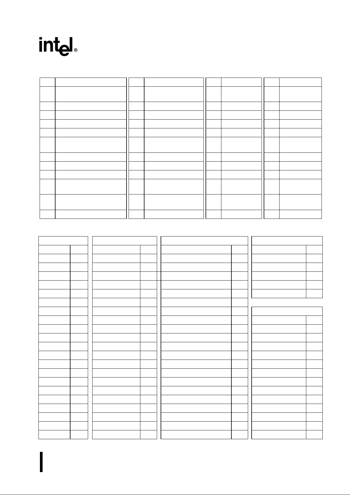
1.0 PRODUCT OVERVIEW
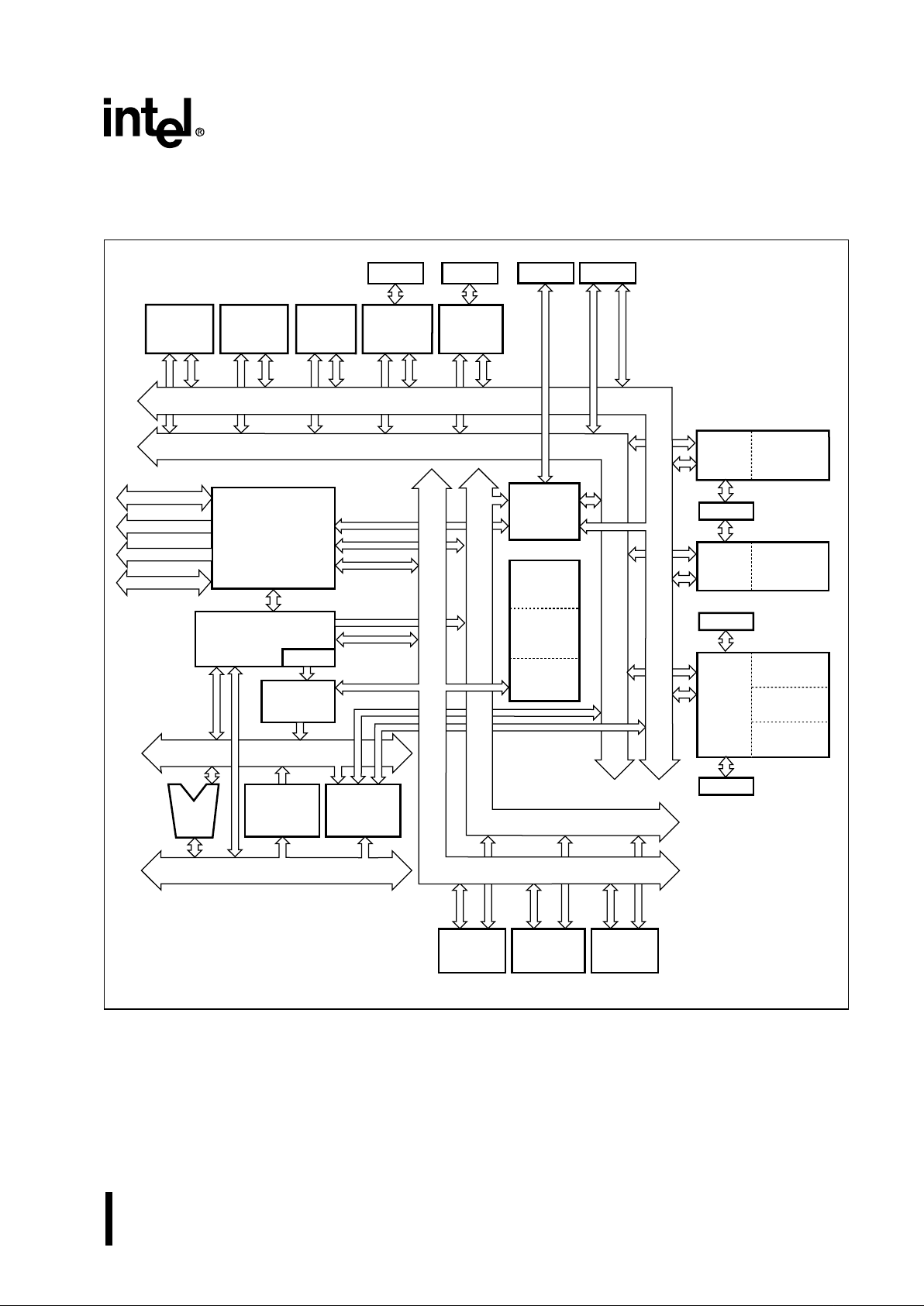
Figure 1. 8xC196EA Block Diagram
The 8xC196EA is highly integrated with an enhanced peripheral set. The serial debug unit (SDU) provides
system debug and development capabilities. The SDU can set a single hardware breakpoint and provides
read and wr ite a cce ss to code RAM throug h a hi gh -spee d, de dica te d seri al lin k. A stac k ove rflow /un der flow
monitor assists in code development by causing an unmaskable interrupt if the stack pointer crosses a
user-defined boundary. The 16-channel A/D converter supports an auto-scan mode that operates with no
Code/Data
RAM
3 Kbytes
EPORT
Queue
A20:16
Source (16)
Destination (16)
AD15:0
SIO0
Baud-rate
Generator
EPA 4 Timers
Ports 7,8
Port 11
17 Capture/
Compares
A/D
Converter
Bus
Controller
A15:0
Serial Debug
Unit
Watchdog
Timer
Stack
Overflow
Module
Pulse-width
Modulators
SSIO0
SSIO1
ROM
8 Kbytes
A3178-03
SIO1
Baud-rate
Generator
Port 10
Bus-Control
Interface Unit
Microcode
Engine
Chip-select
Unit
Peripheral
Transaction
Server
Memory
Interface
Unit
Register
RAM
1 Kbyte
ALU
Interrupt
Controller
Peripheral
Interrupt
Handler
Bus Control
Peripheral Addr Bus (10)
Peripheral Data Bus (16)
Memory Addr Bus (24)
Port 12
8 Output/
Simulcaptures
Port 9
Port 2
Memory Data Bus (16)
Page 8
2 ADVANCE INFORMATION
8xC196EA — AUTOMOTIVE
CPU overhead. Each A/D channel has a dedicated result register. The EPA supports high-speed input
captures and output compares with 17 programmable, high-speed capture/compare channels. Eight
outpu t-on ly ch ann els pr ov ide s uppo rt for time-b ase conv ersio ns by cap turi ng the valu e of one of four time rs
when a compare occurs.
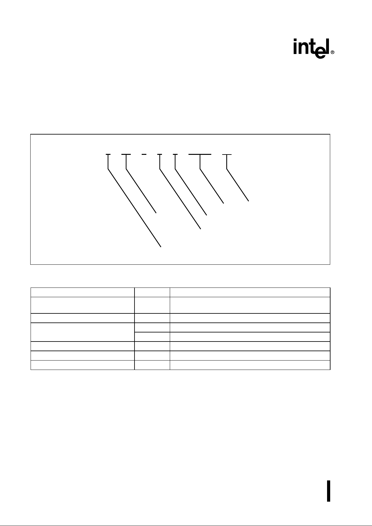
2.0 NOMENCLATURE OVERVIEW
Figure 2. Product Nomenclature
Table 1. Description of Product Nomenclature
Parameter Options Description
Temperature and Burn-in Options A Automotive operating temperature range (–40° C to
125° C c ase) with Intel standard bur n-in.
Packaging Options S QFP
Program Memory Options 3 Internal ROM
0 CPU only - no internal ROM
Process Information C CHMOS
Prod uc t Fam i ly 196EA
Device Speed no mark 40 MHz
A2815-01
Program Memory Options
XXXXX XXXX8XXX
Packaging Options
Temperature and Burn-in Options
Process Information
Product Family
Device Speed
Page 9
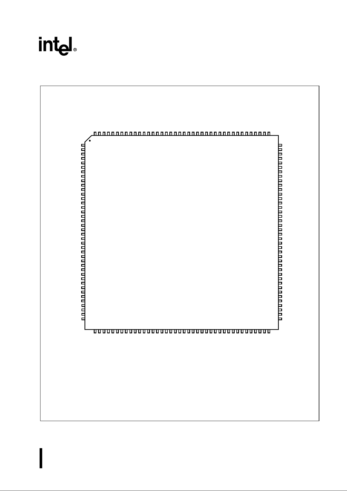
ADVANCE INFORMATION 3
8xC196EA — AUTOMOTIVE
3.0 PINOUT
Figure 3. 8xC196EA 160-p in QFP Pac ka ge
A4461-01
120
119
118
117
116
115
114
113
112
111
110
109
108
107
106
105
104
103
102
101
100
99
98
97
96
95
94
93
92
91
90
89
88
87
86
85
84
83
82
81
AS8xC196EA
View of component as
mounted on PC board
1
2
3
4
5
6
7
8
9
10
11
12
13
14
15
16
17
18
19
20
21
22
23
24
25
26
27
28
29
30
31
32
33
34
35
36
37
38
39
40
41
42
43
44
45
46
47
48
49
50
51
52
53
54
55
56
57
58
59
60
61
62
63
64
65
66
67
68
69
70
71
72
73
74
75
76
77
78
79
80
160
159
158
157
156
155
154
153
152
151
150
149
148
147
146
145
144
143
142
141
140
139
138
137
136
135
134
133
132
131
130
129
128
127
126
125
124
123
122
121
AD0 / P3.0
AD1 / P3.1
AD2 / P3.2
AD3 / P3.3
AD4 / P3.4
AD5 / P3.5
AD6 / P3.6
AD7 / P3.7
V
CC
VCC
V
SS
V
SS
AD8 / P4.0
AD9 / P4.1
AD10 / P4.2
AD11 / P4.3
AD12 / P4.4
AD13 / P4.5
AD14 / P4.6
AD15 / P4.7
P5.7 / RPD
P5.4/BREQ#/TMODE#
P5.6 / READY
P5.1 / INST
P5.0 / ALE
P5.5 / BHE# / WRH#
P5.3 / RD#
P5.2 / WR# / WRL#
V
SS
V
CC
A20 / EPORT.4
A16 / EPORT.0
A17 / EPORT.1
A18 / EPORT.2
A19 / EPORT.3
EPORT.5 / CS0#
EPORT.6 / CS1#
EPORT.7 / CS2#
NC
NC
NC
NC
NC
NC
EA#
V
CC
PLLEN
XTAL2
XTAL1
V
SS
V
CC
P2.7 / CLKOUT
P2.6 / ONCE#
P2.5
P2.4 /RXD1
P2.3 / TXD1
P2.2 / EXTINT
P2.1 / RXD0
P2.0 / TXD0
V
CC
V
SS
CRBUSY#
CROUT
CRIN
CRDCLK
V
CC
NC
V
SS
V
SS
ACH15
ACH14
ACH13
ACH12
ACH11
ACH10
ACH9
ACH8
ACH7
ACH6
NC
A15
A14
A13
A12
A11
A10
A9
A8
V
CC
V
SS
A7
A6
A5
A4
A3
A2
A1
A0
P9.7 / OS7
P9.6 / OS6
P9.5 / OS5
P9.4 / OS4
P9.3 / OS3
P9.2 / OS2
P9.1 / OS1
P9.0 / OS0
P7.0 / EPA0 / T1CLK
P7.1 / EPA1 / T1RST
P7.2 / EPA2 / T2CLK
P7.3 / EPA3 / T2RST
P7.4 / EPA4 / T3CLK
P7.5 / EPA5 / T3RST
V
SS
V
CC
P7.6 / EPA6 / T4CLK
P7.7 / EPA7 / T4RST
P8.7 / EPA15
P8.6 / EPA14
P8.5 / EPA13
NC
P8.4 / EPA12
P8.3 / EPA11
P8.2 / EPA10
P8.1 / EPA9
P8.0 / EPA8
P10.5
P10.4 / EPA16
P10.3 / SD1
P10.2 / SC1 / CHS#
P10.1 / SD0
P10.0 / SC0
P11.4 / PWM4
P11.5 / PWM5
P11.6 / PWM6
P11.7 / PWM7
P11.3 / PWM3
P11.2 / PWM2
P11.1 / PWM1
P11.0 / PWM0
V
SS
V
CC
P12.4
P12.0
P12.1
P12.2
P12.3
V
SS
NC
V
CC
NC
RESET#
NMI
V
REF
ANGND
ACH0
ACH1
ACH2
ACH3
ACH4
ACH5
†
††
This pin supplies voltage to the phase-locked loop circuitry, so use extra care to keep it stable.
This pin supplies voltage to the code RAM. Maintain at 5 volts to retain data in code RAM.
NC pins must be unconnected to prevent accidental entry into a test mode.
† ††
Page 10
4 ADVANCE INFORMATION
8xC196EA — AUTOMOTIVE
Table 2. 8xC196EA 160-pin QFP Package Pin Assignments (Sheet 1 of 2)
Pin Name Pin Name Pin Name Pin Name
1
AD0 / P3.0
41
NC
81
ACH5
121
NC
2
AD1 / P3.1
42
NC
82
ACH4
122
P8.5 / EPA13
3
AD2 / P3.2
43
NC
83
ACH3
123
P8.6 / EPA14
4
AD3 / P3.3
44
NC
84
ACH2
124
P8.7 / EPA15
5
AD4 / P3.4
45
EA#
85
ACH1
125
P7.7 / EPA7 /
T4RST
6
AD5 / P3.5
46
V
CC
86
ACH0
126
P7.6 / EPA6 /
T4CLK
7
AD6 / P3.6
47
PLLEN
87
ANGND
127
V
CC
8
AD7 / P3.7
48
XTAL2
88
V
REF
128
V
SS
9
V
CC
49
XTAL1
89
NMI
129
P7.5 / EPA5 /
T3RST
10
V
CC
50
V
SS
90
RESET#
130
P7.4 / EPA4 /
T3CLK
11
V
SS
51
V
CC
91
NC
131
P7.3 / EPA3 /
T2RST
12
V
SS
52
P2.7 / CLKOUT
92
V
CC
132
P7.2 / EPA2 /
T2CLK
13
AD8 / P4.0
53
P2.6 / ONCE#
93
NC
133
P7.1 / EPA1 /
T1RST
14
AD9 / P4.1
54
P2.5
94
V
SS
134
P7.0 / EPA0 /
T1CLK
15
AD10 / P4.2
55
P2.4 / RXD1
95
P12.3
135
P9.0 / OS0
16
AD11 / P4.3
56
P2.3 / TXD1
96
P12.2
136
P9.1 / OS1
17
AD12 / P4.4
57
P2.2 / EXTINT
97
P12.1
137
P9.2 / OS2
18
AD13 / P4.5
58
P2.1 / RXD0
98
P12.0
138
P9.3 / OS3
19
AD14 / P4.6
59
P2.0 / TXD0
99
P12.4
139
P9.4 / OS4
20
AD15 / P4.7
60
V
CC
100
V
CC
140
P9.5 / OS5
21
P5.7 / RPD
61
V
SS
101
V
SS
141
P9.6 / OS6
22
P5.4/BREQ#/TMODE#
62
CRBUSY#
102
P11.0 /
PWM0
142
P9.7 / OS7
23
P5.6 / READY
63
CROUT
103
P11.1 /
PWM1
143
A0
24
P5.1 / INST
64
CRIN
104
P11.2 /
PWM2
144
A1
25
P5.0 / ALE
65
CRDCLK
105
P11.3 /
PWM3
145
A2
26
P5.5 / BHE# / WRH#
66
V
CC
106
P11.7 /
PWM7
146
A3
27
P5.3 / RD#
67
NC
107
P11.6 /
PWM6
147
A4
28
P5.2 / WR# / WRL#
68
V
SS
108
P11.5 /
PWM5
148
A5
Page 11
ADVANCE INFORMATION 5
8xC196EA — AUTOMOTIVE
29
V
SS
69
V
SS
109
P11. 4 /
PWM4
149
A6
30
V
CC
70
ACH15
110
P10.0 / SC0
150
A7
31
A20 / EPORT.4
71
ACH14
111
P10.1 / SD0
151
V
SS
32
A16 / EPORT.0
72
ACH13
112
P10.2 / SC1
152
V
CC
33
A17 / EPORT.1
73
ACH12
113
P10.3 / SD1
153
A8
34
A18 / EPORT.2
74
ACH11
114
P10. 4 /
EPA16
154
A9
35
A19 / EPORT.3
75
ACH10
115
P10.5
155
A10
36
EPORT.5 / CS0#
76
ACH9
116
P8.0 / EPA8
156
A11
37
EPORT.6 / CS1#
77
ACH8
117
P8.1 / EPA9
157
A12
38
EPORT.7 / CS2#
78
ACH7
118
P8.2 /
EPA10
158
A13
39
NC
79
ACH6
119
P8.3 /
EPA11
159
A14
40
NC
80
NC
120
P8.4 /EPA12
160
A15
Table 3. Pin Assignment Arranged by Functional Categories (Sheet 1 of 2)
Addr & Data Input/Output Input/Output (Cont’d) Input/Output (Cont’d)
Name Pin Name Pin Name Pin Name Pin
A0 143 P2.0 / TXD0 59
EPORT.7 38 P12.0 98
A1 144 P2.1 / RXD0 58
P7.0 / EPA0 / T1CLK 134 P12.1 97
A2 145 P2.2 57
P7.1 / EPA1 / T1RST 133 P12.2 96
A3 146 P2.3 / TXD1 56
P7.2 / EPA2 / T2CLK 132 P12.3 95
A4 147 P2.4 / RXD1 55
P7.3 / EPA3 / T2RST 131 P12.4 99
A5 148 P2.5 54
P7.4 / EPA4 / T3CLK 130
A6 149 P2.6 53 P7.5 / EPA5 / T3RST 129 Analog Inputs
A7 150 P2.7 52
P7.6 / EPA6 / T4CLK 126 Name Pin
A8 153 P3.0 1
P7.7 / EPA7 / T4RST 125 ACH0 86
A9 154
P3.1 2 P8.0 / EPA8 116 ACH1 85
A10 155 R3.2 3
P8.1 / EPA9 117 ACH2 84
A11 156 P3.3 4
P8.2 / EPA10 118 ACH3 83
A12 157
P3.4 5 P8.3 / EPA11 119 ACH4 82
A13 158 P3.5 6
P8.4 / EPA12 120 ACH5 81
A14 159 P3.6 7
P8.5 / EPA13 122 ACH6 79
A15 160 P3.7 8
P8.6 / EPA14 123 ACH7 78
A16 32 P4.0 13
P8.7 / EPA15 124 ACH8 77
A17 33 P4.1 14
P9.0 / OS0 135 ACH9 76
A18 34 P4.2 15
P9.1 / OS1 136 ACH10 75
A19 35 P4.3 16
P9.2 / OS2 137 ACH11 74
A20 31 P4.4 17
P9.3 / OS3 138 ACH12 73
Table 2. 8xC196EA 160-pin QFP Package Pin Assignments (Sheet 2 of 2)
Pin Name Pin Name Pin Name Pin Name
Page 12
6 ADVANCE INFORMATION
8xC196EA — AUTOMOTIVE
AD0 1 P4.5 18 P9.4 / OS4 139 ACH13 72
AD1 2 P4.6 19
P9.5 / OS5 140 ACH14 71
AD2 3 P4.7 20
P9.6 / OS6 141 ACH15 70
AD3 4
P5.0 25 P9.7 / OS7 142
AD4 5 P5.1 24
P10.0 / SC0 110 Bus Control & Status
AD5 6 P5.2 28
P10.1 / SD0 111 Name Pin
AD6 7 P5.3 27
P10.2 / SC1 112 ALE 25
AD7 8 P5.4 22
P10.3 / SD1 113 BHE#/WRH# 26
AD8 13 P5.5 26
P10.4 / EPA16 114 BREQ# 22
AD9 14 P5.6 23
P10.5 115 CS0# 36
AD10 15
P5.7 21 P11.0 / PWM 0 102 CS1# 37
AD11 16
EPORT.0 32 P11.1 / PWM1 103 CS2# 38
AD12 17
EPORT.1 33 P11.2 / PWM2 104 INST 24
AD13 18
EPORT.2 34 P11.3 / PWM3 105 RD# 27
AD14 19
EPORT.3 35 P11.4 / PWM4 109 READY 23
AD15 20
EPORT.4 31 P11.5 / PWM5 108
EPORT.5 36 P11.6 / PWM6 107
EPORT.6 37 P11.7 / PWM7 106 WR#/WRL# 28
Power & Ground Processor Control
Name
Pins Name P in
ANGND
87 CLKOUT 52
V
CC
9, 10, 30, 46†, 51, 60, 66††, 92, 100, 12 7, 152 EA# 45
V
SS
11, 12, 29, 50, 61, 68, 69, 94, 101, 128, 151 EXTINT 57
V
REF
88 NMI 89
ONCE# 53
No Connection PLLEN 47
Name
Pins RESET# 90
NC
†††
39–44, 67, 69, 80, 91, 93, 121 RPD 21
TMODE# 22
XTAL1 49
XTAL2 48
†
This pin supplies voltage to the phase-locked loop circuitry, so use extra
care to keep it stable.
††
This pi n su pplies volt ag e t o co de RAM . To r et ai n data, main ta in 5 volts .
†††
Alway s leave N C (no connect) pins unconne c ted to prevent accidental
entr y in to tes t mo de s .
Code Debug
Name P in
CRBUSY# 62
CRDCLK 65
CRIN 64
CROUT 63
Table 3. Pin Assignment Arranged by Functional Categories (Sheet 2 of 2)
Page 13

ADVANCE INFORMATION 7
8xC196EA — AUTOMOTIVE
4.0 SIGNALS
Table 4. Signal Descriptions (Sheet 1 of 8)
Name Type Description
A15:0 O System Addr ess Bus
These address lines provide address bits 0–15 during the entire external memory cycle during both multi plexed and demultip lexed bus modes.
A20:16 I/O Address Lines 16 –20
These address lines provide address bits 16–20 during the entire external
memory cycle, supporting extended addressing of the 2 Mbyte address space.
NOTE: Internally, there are 24 address bits; however, only 21 external
address pins (A20:0) are implemented. The internal address space is
16 Mbytes (000000FFFFFFH) and the external address space is
2 Mbytes (00000 1FFFFFH). The device resets to FF2080H in internal
memory or 1F2 080H in external memory.
A20:16 are multiplexed with EPORT.4:0.
ACH15:0 I Analog Channels
These pins are analog inputs to the A/D converter.
The ANGND and V
REF
pins must be connected for the A/D conv erter to function.
AD15:0 I/O Address/Data Lines
The function of these pins depend on the bus size and mode. When a bus
access is not occurring, these pins revert to their I/O port function.
16-bit Multiplexed Bus Mode:
AD15:0 dr i ve a ddr ess bi ts 0–1 5 dur i ng the f ir s t hal f o f the bu s cyc le an d dri ve or
receive data during the second half of the bus cycle.
8-bit Multiplexed Bus Mode:
AD15:8 drive address bits 8–15 during the entire bus cycle. AD7:0 drive
address bits 0–7 during the first half of the bus cycle and drive or receive data
during the second half of the bus cycle.
16-bit Demultiplexed Mode:
AD15 :0 dri v e or receive data dur ing the entire bus cycle .
8-bit Demultiplexe d Mo de :
AD7:0 drive or receive data during the entire bus cycle. AD15:8 drive the data
that is currently on the high byte of th e internal bus.
AD7:0 share package pins P3.7:0. AD15:8 share package pi ns P4.7:0.
ALE O Address Latch Enable
This active-high output signal is asserted only during external memory cycles.
ALE signals the start of an external bus cycle and indicates that valid address
information is available on the system address/data bus (A20:16 and AD15:0
for a multipl exed bus; A20:0 for a demultiplexed bus).
An external latch can use this signal to demultiplex address bits 0–15 from the
address/data bus in multiplexed mode.
ALE sh ares a package pin with P5.0.
ANGND GND Analog Ground
ANGND must be connected for A/D converte r operation . ANGND and V
SS
should be nominally at the same potential.
Page 14

8 ADVANCE INFORMATION
8xC196EA — AUTOMOTIVE
BHE# O Byte High Enable
†
During 16-bit bus cycles, this active-low output signal is asserted for word and
high-byte reads and writes to external memory. BHE # indicates that val id data
is being transferred over the upper half of the system data bus. Use BHE#, in
conjunction with AD0, to determine which memory byte is being transferred
over the system bus:
BHE# AD0 Byte(s) Accessed
0 0 both bytes
0 1 high by te on ly
1 0 low byte on ly
BHE# shares a package pin with P5.5 and WRH#.
†
The chip configuration register 0 (CCR0) determines whether this pin functions as BHE# or WRH#. CCR0.2 = 1 selects BHE#; CCR0.2 = 0 selects
WRH#.
BREQ# O Bus Request
This active-low output s ignal is asserted during a hold cyc le when the bus controller has a pending external memory cycle.
You must enable the bus-hold protocol before using this signal.
BREQ# shares a package pin with P5.4.
CLKOUT O Clock Output
Output of the internal clock generator. The CLKOUT frequency can be programmed to one of five frequencies: the internal opera ting frequency (f) divided
by a factor of two, four, eight, o r sixteen, or the same frequency as the oscillator
input (F
XTAL1
). CLKOU T has a 50% dut y cy c le.
CLKOUT shares a package pin with P2.7
CRBUSY# O Code RAM Busy
This signal indicates that the serial debug unit (SDU) is not ready to conduct a
transaction.
CRDCLK I Code RAM Clock
Provides the clock signal for the serial debug unit (SDU). The maximum clock
frequency equals the ope rating frequency (f ) divi ded by tw o.
CRIN I Code RAM Data Input
Serial input for test instructions and data into the serial debug unit (SDU). Data
is transferred in 8-bit bytes with the most-significant bit (MSB) first. Each bit is
sampled on the rising edge of CRDCLK.
CROUT O Code RAM Data Output
Serial output for data from the serial debug unit (SDU). Data is transferred in
8-bit bytes with the most-significant bit (MSB) first. Each bit is valid on the rising
edge of CRDCLK.
Table 4. Signal Descriptions (Sheet 2 of 8)
Name Type Description
Page 15

ADVANCE INFORMATION 9
8xC196EA — AUTOMOTIVE
CS2:0# O Chip-select Lines 0–2
The active-low output CS
x
# is asserted during an external memory cycle when
the address to be accessed is in the range programmed for chip select
x
. If the
external memory address is outside the range assigned to the three chip
selects, no c hip-select output is asserted and the bus con figuration defaults to
the CS2# values.
Immediately following reset, C S0# is automatically assigned to the range
FF2000 FF20FFH (1F2000 1F20FFH if external).
CS2:0# share package pins with EPO RT.7:5.
EA# I External Access
This input determines whet her memory acce sses to sp ecial-purpose and program memory partitions (FF2000 FF3FFFH) are directed to internal or external
memory. These accesses are directed to internal memory if EA# is held high
and to external memory if EA# is held low. For an access to any other memory
location, the value of EA# is irrelevant.
EA# is sampled and latched onl y on the rising edge of RESET#. Changin g the
level of EA# after reset has no effect.
On devices with no internal nonvolatile memory, always connect EA# to V
SS
.
EPA16:0 I/O Event Process or Array (EPA) Capture/Co mpa re Channels
High-speed input/output signals for the EPA capture/compare channels.
EPA16:0 share package pins with the following signals: EPA0/P7.0/T1CLK,
EPA1/P7.1/T1RST, EPA2/P7.2/T2CLK, EPA3/P7.3/T2RST,
EPA4/P7.4/T3CLK, EPA5/P7.5/T3RST, EPA6/P7.6/T4CLK,
EPA7/P7.7/T4RST, EPA8/P8.0, EPA9/P8.1, EPA10/P8.2, EPA11/P8.3,
EPA12/P8.4, EPA13/P8.5, EPA14/P8.6, EPA15/P8.7, and EPA16/P10.4.
EPORT.7:0 I/O Extended Addressing Port
This is a standard 8- bit, bidir ectional port.
EPORT.4:0 share package pins with A20:16. EPORT7:5 share package pins
with CS2:0#.
EXTINT I External Interrupt
In normal operating mode, a rising edge on EXTINT sets the EXTINT interrupt
pending bit. EXTINT is sampled during phase 2 (CLKOUT high). The minimum
high time is one state time.
In pow erdown mode, asserting the EXTINT si gnal for at least 5 0ns causes the
device to resume normal operation. The interrupt need not be enabled, but the
pin must be configured as a special-function input. If the EXTINT interrupt is
enabled, the CPU executes the interrupt service routine. Othe rwise, the CPU
exec utes t he instruction that immediately follows the command that invoked the
power-saving mode.
In idle mode, asser ting an y enabled interrupt c auses the device to resume normal operation.
EXTINT shares a package pin with P2.2.
Table 4. Signal Descriptions (Sheet 3 of 8)
Name Type Description
Page 16

10 ADVANCE INFORMATION
8xC196EA — AUTOMOTIVE
INST O Instruction Fetch
This active-high output signal is valid only during external memory bus cycles.
When high, INST indicates that an instruction is bei ng fetched from ext ernal
memory. The signal remains high during the entire bus cy cle of an ex ternal
instr uction fetch. INST is low for data accesses, including interrupt vector
fetches and chip configuration byte reads. INST is low dur ing internal memory
fetc hes.
INST shares a package pin with P5.1.
NMI I Nonmaskable Interrupt
In normal op erating mode, a rising edge on NMI generates a nonmaskable
interrupt. NMI has the highest priority of all prioritized interrupts. Assert NMI for
greater than one state time to guarantee that it is recognized.
ONCE# I On-circuit Emulation
Holding ONCE# low during the rising edge of RESET# places the device into
on-circuit emulation (ONCE) mode. PLLEN must also be held low. This mode
puts all pins into a high- impedance state, th ereby isolating t he device from
other components in the system. The value of ONCE# is latched when the
RESET# pin goes inac tive. W hile the device is in ONCE mode, you can debug
the sys te m us in g a cli p- o n em ul ator.
To exit ONCE mode, reset the d evice by pulling the R ESET# signal low. To prevent in ad ve rte nt e nt ry i nt o O NCE m od e, eit he r con f ig ure th is pi n as a n o ut put or
hold it hig h during r es et and en su r e that yo ur sy s tem me et s t he V
IH
spec ifica-
tion.
ONCE # sh ar e s a pack ag e pin with P2. 6.
OS7:0 O Event Processor Array (EPA) Compare-only Channels with Simulcapture
Outputs of the EPA’s compare-only channels. These pins are multiplexed with
port 9 and may be configured as standard I/O.
OS7:0 share package pins with P9.7:0.
P2.7:0 I/O Port 2
This is a standard, 8-bit, bidirect ional port that is multipl exed wi th individually
select ab le sp ec ia l-f un cti on si gn als. P2. 6 is mu lti pl exed w ith ON CE#. T o pr eve nt
inadve rte nt en tr y i nto ON CE mo de, ei t her c on fig ur e this pi n a s a n o utpu t or h ol d
it high during reset and ensure that your system me ets the V
IH
specificat ion.
Port 2 shares package pins with the following signals: P2.0/TXD0, P2.1/RXD0,
P2.2/EXTINT, P2.3/TXD1, P2.4/RXD1, P2.6/ONCE#, and P2.7/CLKOUT.
P3.7:0 I/O Port 3
This is a memory-ma pped, 8-bit, bidi rectional port with programmable
open-drain or complementary output modes. The pins are shared with the multiplexed address/data bu s, which has complementary drivers.
P3.7:0 share package pins with AD7:0.
P4.7:0 I/O Port 4
This is a memory-ma pped, 8-bit, bidi rectional port with programmable
open-drain or complementary output modes. The pins are shared with the multiplexed address/data bu s, which has complementary drivers.
P4.7:0 share package pins with AD15:8.
Table 4. Signal Descriptions (Sheet 4 of 8)
Name Type Description
Page 17

ADVANCE INFORMATION 11
8xC196EA — AUTOMOTIVE
P5.7:0 I/O Port 5
This is a memory-mapped, 8-bit, bidirectional port that is multiplexed with individually se lectable cont rol signals. P5.4 is multiplexed with TMOD E#. If this pin
is held low during reset, the device will enter a test mode. To prevent inadvertent entry int o a reserved test mode, either confi gure this pin as an output or
hold it high during reset and ensure that your sys tem meet s the V
IH
specifica-
tion.
Port 5 shares package pins with the following signals: P5.0/ALE, P5.1/INST,
P5.2/WR#/WRL#, P5.3/RD#, P5.4/BREQ#/TMODE#, P5.5/BHE#/WRH#,
P5.6/READY, and P5.7/RPD.
P7.7:0 I/O Port 7
This is a standard, 8-bit, bidirectional port that is multiplexed with individually
selectable special-function signals.
Port 7 share s package pins with th e following signals: P7.0/EPA0/T1CLK,
P7.1/EPA1/T1RST, P7.2/EPA2/T2CLK, P7.3/EPA3/T2RST,
P7.4/EPA4/T3CLK, P7.5/EPA5/T3RST, P7.6/EPA6/T4CLK, and
P7.7/EPA7/T4RST.
P8.7:0 I/O Port 8
This is a standard, 8-bit, bidirectional port that is multiplexed with individually
selectable special-function signals.
P8.7: 0 share package pins with EPA15:8.
P9.7:0 I/O Port 9
This is a standard, 8-bit, bidirectional port that is multiplexed with individually
selectable special-function signals.
P9.7: 0 share package pins with OS7:0.
P10.5:0 I/O Port 10
This is a standard, 6-bit, bidirectional port that is multiplexed with individually
selectable special-function signals.
Port 10 shares package pins with the following signals: P10.0/SC0, P10.1/SD0,
P10.2/SC1, P10.3/SD1, P10.4/EPA16, and P10.5.
P11.7:0 I/O Port 11
This is a standard, 8-bit, bidirectional port that is multiplexed with individually
selectable special-function signals.
P11.7:0 share package pins with PWM7:0.
P12.4:0 I/O Port 12
This is a memory-m apped, 5-bit, b idirectiona l por t. P12.2:0 select the test-R OM
exec ution mo de.
PLLEN I Phase-locked Loop Enable
This active-high input pin enables the on-chip clock doubler.
This pin must be held l ow when enteri ng on-c ircuit emulation (ON CE) mod e.
PWM7: 0 O Pulse Width Modu lator Outputs
These are PWM output pins with high-current drive capability.
PWM7:0 share package pins with P11.7:0.
Table 4. Signal Descriptions (Sheet 5 of 8)
Name Type Description
Page 18

12 ADVANCE INFORMATION
8xC196EA — AUTOMOTIVE
RD# O Read
Read-signal output to external memory. RD# is asserted only during external
memory reads.
RD# shares a pa ckage pin with P5.3.
READY I Ready Input
This active-high input signal is used to lengthen ex ternal memory cycl es for
slow memory by generating wait states in addition to the wait states that are
generated internally.
When READY is high, CPU operation continues in a normal manner wit h wait
states inserted as programmed in the chip configuration registers or the
chip-select
x
bus control register. READY is ignored for all internal memory
accesses.
READ Y sh ares a packag e pin with P5. 6.
RESET# I/O Reset
A level-sensitive reset input to and open-drain system reset output from the
microcontroller. Either a falling edge on RESET# or an internal reset turns on a
pull-down transistor connected to the RESET# pin for 16 state times. In the
powerdown and idle modes, asserting RESET# causes the chip to reset and
return to norm al operating mode. After a device reset, the f irst instru ction f etch
is from FF2080H (or 1F2080H in external memory ).
RPD I Return from Powerdown
Timing pin f or the return-from- powerdown circuit.
If your application uses powerdown mode, connect a capacitor between RPD
and V
SS
if either of the following conditions are true.
• the intern al oscillator is the clock source
• the phase-locked loop (PLL) circuitry is enabled (see PLLEN signal
description)
The capacitor causes a delay that enables the oscillator and PLL circuitry to
stabilize before the internal CPU and peripheral clocks are ena bled.
The capacitor is not required if your application uses powerdown mode and if
both of the following conditions are true.
• an external clock input is the clock source
• the phase-locked loop circuitry is disabled
If your application does not use powerdown mode, leave this pin unconnected.
RPD shares a package pi n with P5.7.
RXD1:0 I/O Receive Serial Data 0 and 1
In modes 1, 2, and 3, RXD0 and 1 receive serial port input data. In mode 0, they
functions as either inputs or open- drain outputs for data.
RXD0 shares a package pin with P2.1 and RXD1 shares a package pin with
P2.4.
SC1:0 I/O Clock Pins for SSIO0 and 1
For handshaking mode, configure SC1:0 as open-drain outputs.
This pin carries a si gnal only during receptions and transmissions. When the
SSIO port is idle, the pin remains either high (with handshaking) or low (without
handshaking).
SC0 shares a package pin with P10.0, and SC1 shares a package pin with
P10.2.
Table 4. Signal Descriptions (Sheet 6 of 8)
Name Type Description
Page 19

ADVANCE INFORMATION 13
8xC196EA — AUTOMOTIVE
SD1:0 I/O Data Pins for SSIO0 and 1
These pins are the data I/O pins for SSIO0 and 1.
SD0 shares a package pin with P10.1, and SD1 shares a package pin with
P10.1.
T1CLK I Timer 1 External Clock
Exter nal clock fo r Timer 1.Tim er 1 is programmable to incr ement or decement
on the rising edge, the falling edge, or both rising and falling edges of T1CLK.
T1CL K shares a package pin with P7.0 and EPA0.
T2CLK I Timer 2 External Clock
External clock for timer 2. Timer 2 is prog rammab le to increment or dece ment
on the rising edge, the falling edge, or both rising and falling edges of T2CLK.
External clock for the serial I/O baud-rate generator input (program selectable).
T2CL K shares a package pin with P7.2 and EPA2.
T3CLK I Timer 3 External Clock
External clock for timer 3. Timer 3 is prog rammab le to increment or dece ment
on the rising edge, the falling edge, or both rising and falling edges of T3CLK.
T3CL K shares a package pin with P7.4 and EPA4.
T4CLK I Timer 4 External Clock
External clock for timer 4. Timer 2 is prog rammab le to increment or dece ment
on the rising edge, the falling edge, or both rising and falling edges of T4CLK.
T4CL K shares a package pin with P7.6 and EPA6.
T1RST I Timer 1 External Reset
Exter nal re set for timer 1. Timer 1 is programmable to reset on the rising edge,
the falling edge, or both rising and falling edges of T1RST.
T1RST share s a package pin with P7.1 and EP A1.
T2RST I Timer 2 External Reset
Exter nal re set for timer 2. Timer 2 is programmable to reset on the rising edge,
the falling edge, or both rising and falling edges of T2RST.
T2RST share s a package pin with P7.3 and EP A3.
T3RST I Timer 3 External Reset
Exter nal re set for timer 3. Timer 3 is programmable to reset on the rising edge,
the falling edge, or both rising and falling edges of T3RST.
T3RST share s a package pin with P7.5 and EP A5.
T4RST I Timer 4 External Reset
Exter nal re set for timer 4. Timer 4 is programmable to reset on the rising edge,
the falling edge, or both rising and falling edges of T4RST.
T4RST share s a package pin with P7.6 and EP A6.
TMODE# I Test-Mode Entry
If this pin is held low during reset, the device will enter a test mode. The value of
several other pins defines the actual test mode. All test modes, except
test-ROM execution, are reserved for Intel factory use. If you choose to configure t his signal as an input, always hold it high during r eset and ensure that your
system meets the V
IH
specification to prevent inadvertent entry into test mode.
TMODE# shares a package pin with P5.4 and BREQ#.
Table 4. Signal Descriptions (Sheet 7 of 8)
Name Type Description
Page 20

14 ADVANCE INFORMATION
8xC196EA — AUTOMOTIVE
TXD1:0 O Transmit Serial Data 0 and 1
In serial I/O modes 1, 2, and 3, TXD0 and 1 transmit serial port output data. In
mode 0, they are the serial clock output.
TXD0 s hares a packag e pin with P2.0 and TXD1 shares a packa ge pin with
P2.3.
V
CC
PWR Digital Supply Voltage
Connect each V
CC
pin to the digital s upply voltage.
V
REF
PWR Reference Voltage for the A/D Converter
This pin also suppl ies operating voltage to t he analog portion of the A/D converter .
V
SS
GND Digital Circuit Ground
These pins supply ground for the digital circuitry. Connect each V
SS
pin to
grou nd through the low e st po ss i ble imped an c e path.
WR# O Wr ite
†
This act i ve -lo w out p ut in di ca te s tha t an ex ter n al w rit e i s o ccur r ing. Th is sign al is
asserted only during external memory writes .
WR# is multiplexed with P5.2 and WRL#.
†
The chip configuration register 0 (CCR0) determines whether this pin functions as WR# or WRL#. CCR0.2 = 1 selects WR#; CCR0.2 = 0 selects WRL#.
WRH# O Write High
†
During 16-bit bus cycles, this active-low output signal is asserted for high-byte
writes and word writes to external memory. During 8-bit bus cycles, WRH# is
asserted for all write operations.
WRH# shares a package pin with P5.5 and BHE#.
†
The chip configuration register 0 (CCR0) determines whether this pin functions as BHE# or WRH#. CCR0.2 = 1 selects BHE#; CCR0.2 = 0 selects
WRH#.
WRL# O Write Low
†
During 16-bit bus cycles, this active-low output signal is asserted for low-byte
writes and word writes to external memory. During 8-bit bus cycles, WRL# is
asserted for all write operations.
WRL# sh ares a package pin with P5.2 and WR#.
†
The chip configuration register 0 (CCR0) determines whether this pin functions as WR# or WRL#. CCR0.2 = 1 selects WR#; CCR0.2 = 0 selects WRL#.
XTAL1 I Input Crystal/Resonator or External Clock Input
Input to the on-chip osci llator and the int ernal clock ge nera tors. The intern al
clock generators provide the peripheral clocks, CPU clock, and CLKOUT signal. When using an external clock source instead of the on-chip oscillator, connect the clock input to XTAL1. The external clock s ignal must meet t he V
IH
specification for XTAL1.
XTAL2 O Inverted Output for the Crystal/Res o nator
Outpu t of t he on- chip oscillator inverter. Leave XTAL2 floa ting when the design
uses an exter nal clock source instead of the on-chip oscillator.
Table 4. Signal Descriptions (Sheet 8 of 8)
Name Type Description
Page 21

ADVANCE INFORMATION 15
8xC196EA — AUTOMOTIVE
5.0 ADDRESS MAP
Table 5. 8xC196EA Address Map (She et 1 of 2)
Hex
Address
Descript ion (Note 1, Note 2)
Addressing
Modes
FFFFFF
FF4000
Exter nal device (memory or I/O) connected to address/data bus
Indirect, indexed,
extended
FF3FFF
FF2400
Program memory (Note 3)
Indirect, indexed,
extended
FF23FF
FF2200
Program memory (Note 3)
Indirect, indexed,
extended
FF21FF
FF20C0
Special-purpose memo ry (PIH vectors; Note 3)
Indirect, indexed,
extended
FF20BF
FF2080
Program memory (Note 3);
(After reset, the first instruction is fetched from FF2080H.)
Indirect, indexed,
extended
FF207F
FF2000
Special-purpose memory (CCBs, interrupt vectors, PTS vectors; Note 3)
Indirect, indexed,
extended
FF1FFF
FF1000
Exter nal device (memory or I/O) connected to address/data bus
Indirect, indexed,
extended
FF0FFF
FF0400
Internal code/data RAM (identically mapped from page 00H)
Indirect, indexed,
extended
FF03FF
FF0000
Reserved for in-ci rcuit emulators —
FEFFFF
1F0000
Overlaid memory (reserved for future devices);
locations
x
F0000–xF03FFH are reserved for in-circuit emulators
Indirect, indexed,
extended
1EFFFF
004000
Exter nal device (memory or I/O) connected to address/data bus
Indirect, indexed,
extended
003FFF
002400
A copy of internal ROM (FF2400–FF3FFFH) if CCB1.2=0
External memory if CCB1.2=1
Indirect, indexed,
extended
0023FF
002000
Exter nal device (memory or I/O) connected to address/data bus
Indirect, indexed,
extended
001FFF
001FE 0
Memory-mapped special-function registers (SFRs)
Indirect, indexed,
extended
001FD F
001C0 0
Periphera l special-function registers (SFRs)
Indirect, indexed,
exte nded,
wind owed direct
001BFF
001000
Exter nal device (memory or I/O) connected to address/data bus
Indirect, indexed,
extended
000FFF
000400
Inter nal code/data RAM (identically mapped into page FFH)
Indirect, indexed,
extended
NOTES:
1. Unless otherwise noted, writ e 0FFH to reserved memory locations and write 0 to reserved SFR bits.
2. The contents or functions of reserved locations may change in future device revisions, in which case a
progr am that relies on one or more of thes e locations might not function properly .
3. External memory if EA# is low; internal ROM if EA# is high.
Page 22

16 ADVANCE INFORMATION
8xC196EA — AUTOMOTIVE
0003FF
000100
Upper register file (general-purpose register RAM)
Indi rect , in dexe d,
wind owed direc t
0000FF
00001A
Lower register file (general-purpose register RAM)
Direct, indirect,
indexed
000019
000000
Lower register file (stack pointer and CPU SFRs)
Direct, indirect,
indexed
Table 5. 8xC196EA Address Map (Sheet 2 of 2)
Hex
Address
Description (Note 1, Note 2)
Addressing
Modes
NOTES:
1. Unless otherwise noted, write 0FFH to reserved memory locations and write 0 to reserved SFR bits.
2. The content s or func tions of reserved locat ions may change in future device revisions, in which cas e a
program that relies on one or more of these locations might not function properly.
3. External memory if EA# is low; internal ROM if EA# is high.
Page 23

ADVANCE INFORMATION 17
8xC196EA — AUTOMOTIVE
6.0 ELECTRICAL CHARACTERISTICS
6.1 DC Characteristics
ABSOLUTE MAXIMUM RATINGS
†
Storage Temperatur e .... .............................. –60°C to +150°C
Supply Voltage with Respect to V
SS
............... –0.5 V to +7.0 V
Power Dissipation .......................................................... 1.5 W
OPERATING CONDITIONS
†
TC (Case Temperature Under Bias) .............. –40°C to +125°C
V
CC
(Digital Supply Voltage) .............................. 4.5 V to 5.5 V
V
REF
(Analog Supply Voltage) ........................... 4.5 V to 5.5 V
F
XTAL1
(Input frequency for VCC = 4.5 V – 5.5 V)
(Note 1)................................................ 20 MHz to 40 MHz
NOTE:
1. Thi s de vice is sta ti c an d sh ould opera t e belo w
1 Hz, but has been tested only d own to 20 MHz.
NOTICE: This document contains infor m ation on
products in the des ign phase of development. Th e
specif i cat i ons ar e su bj ec t to ch an ge wit h out n ot i ce .
Verify with your local Intel sales office that you
have the latest datasheet before finalizing a
design.
†
WARNING:
Stressing the device beyond the
“Absolute Maximum Ratings” may cause permanent damage. These are stress r atings only. Operation beyond the “Operating Conditions” is not
recommended and extended exposure beyond the
“Operating Conditions” may affect device
reliability.
Table 6. DC Charact eristics at VCC = 4.5 V – 5.5 V (Sheet 1 of 2)
Symbol Parameter Min
Typical
(Note 1)
Max Units
Test
Conditions
I
CC
VCC supply current 120 135 mA XTAL1 = 40 MHz
V
CC
= 5.5 V
Device in Reset
I
IDLE
Idle mode current 60 95 mA XTAL1 = 40 MHz
V
CC
= 5.5 V
I
PD
Powerdown mode current 50 µA V
CC
= 5.5 V
I
REF
A/D reference supply current
5 mA XTAL1 = 40 MHz
V
CC
= V
REF
= 5.5 V
Device in Reset
I
CRVCC
Code RAM VCC Supply Current
110 µA VCC=5.5 V
I
INJD
Maximum injection current
per port on bidirectional pins
(Note 4)
–10 10 mA
NOTES:
1. Typical values are based on a limited number of samples and are not guaranteed. The values listed are
at room temp eratu re with V
CC
= 5.0 V.
2. For P2.7:0, P3.7:0, P4.7:0, P5.7:0, P6.7:0, P10.3:0, P11.7:0, P12.4:0, AD15:0, EA#, RESET#, PLLEN,
NMI, TDI, TCLK, ONCE#, and XTAL1.
3. For P7.7:0, P8.7:0, P9.7:0, and P10.5:4.
4. The maximum injection current is not tested. The device is designed to meet this specification.
5. Pin capacitance is not te sted. This valu e is based on des ign simulations.
Page 24

18 ADVANCE INFORMATION
8xC196EA — AUTOMOTIVE
I
LI
Input leakag e cu r re nt
(Standard inputs except
analog inputs)
–10 10 µA VSS < VIN < V
CC
I
LI1
Input leakag e cu r re nt
(analog inputs)
–300 300 nA VSS + 100 mV < VIN <
V
REF
– 100 mV
I
IH
Input high current
(NMI only)
175 µA NMI = VCC = 5.5 V
V
IL1
Input low volt ag e (Note 2) –0.5 0.3 V
CC
V
V
IH1
Input high vol tag e (Note 2) 0.7 V
CC
VCC + 0.5 V
V
IL2
Input low volt ag e (Note 3) –0.5 0.4 V
CC
V
V
IH2
Input high vol tag e (Note 3) 0.7 V
CC
VCC + 0.5 V
V
OL1
Output low voltage (output
configured as complementary)
0.3
0.45
1.5
V
V
V
I
OL
= 200 µA
I
OL
= 3.2 mA
I
OL
= 7.0 mA
V
OH1
Output high voltage (output
configured as complementary)
VCC – 0.3
V
CC
– 0.7
V
CC
– 1.5
V
V
V
I
OH
= –200 µA
I
OH
= –3.2 mA
I
OH
= –7.0 mA
V
OL2
Output low voltage in reset 0.5 V I
OL
= 15 µA
I
OH2
Output high current in reset –30
–65
–75
–120
–240
–280
µA
µA
µA
V
OH2
= VCC – 1.0V
V
OH2
= VCC – 2.5V
V
OH2
= VCC – 4.0V
I
OH3
Output high current in reset
on Port 11
-5
-8
-10
–50
–110
–130
µA
µA
µA
V
OH3
= VCC – 1.0V
V
OH3
= VCC – 2.5V
V
OH3
= VCC – 4.0V
V
OH2
Output high voltage in reset VCC – 1 V IOH = –15 µA
V
HYS
Hysteresis vo ltage o n all
inputs except XTAL1
700 mV
C
S
Pin Capacitance (any pin t o
V
SS
) (Note 5)
10 pF
R
RST
Pull-up resistor on RESET#
pin
995kΩV
CC
= 5.5 V,
V
IN
= 4.0 V
Table 6. DC Characteristics at V
CC
= 4.5 V – 5.5 V (Sheet 2 of 2)
Symbol Parameter Min
Typical
(Note 1)
Max Units
Test
Conditions
NOTES:
1. Typical valu es a re ba sed on a lim ited nu mbe r of samp les an d ar e not gu aran t ee d. Th e va lu es lis te d ar e
at room temperature with V
CC
= 5.0 V.
2. For P2.7:0, P3.7:0, P4.7:0, P5.7:0, P6.7:0, P10.3:0, P11.7:0, P12.4:0, AD15:0, EA#, RESET#, PLLEN,
NMI, TDI, TCLK, ON CE#, and XTAL1.
3. For P7.7:0, P8.7:0, P9.7:0, and P10.5:4.
4. The maximum injection current is not tested. The device is designed to meet this specification.
5. Pin capacitance is not tes ted. This value is based on design simulati ons.
Page 25

ADVANCE INFORMATION 19
8xC196EA — AUTOMOTIVE
6.2 AC Characteristics — Multiplexed Bus Mode
Test Conditions: Capacitive load on all pins = 50 pF, Rise and Fall Times = 3 ns.
Table 7. AC Characteristics, Multiplexed Bus Mode (Sheet 1 of 2)
Symbol Parameter Min Max Units
F
XTAL1
Frequency on XT AL1, PLL in 1x mode 20 40 MHz (1, 8)
Frequency on XT AL1, PLL in 2x mode 10 20 MHz (8)
f
Operating freque ncy, f = F
XTAL1
; PLL in 1x mode
20 40 MHz (8)
Operating freque ncy, f = 2F
XTAL1
; PLL in 2x mod e
t Period, t = 1/f 25 50 ns
T
AVDV
Address Valid to Input Data Valid 3t – 40 ns (2)
T
RLDV
RD# Low to Input Data Valid t – 18 ns (2)
T
CHDV
CLKOUT High to Input Data valid 2t – 35 ns (9)
T
RHDZ
RD# High to Input Data Float t + 5 ns
T
RXDX
Data Hold after RD# Inactive 0 ns
T
XHCH
XTAL1 Rising Edge to CLKOUT High or Low 3 50 ns (9)
T
CLCL
CLKOUT Cycle Time 2t ns (9)
T
CHCL
CLKOUT High Period t – 10 t + 10 ns (9)
T
CLLH
CLKOUT Falling to ALE Rising – 10 10 ns (9)
T
LLCH
ALE Falling to CLKOUT Rising – 10 10 ns (9)
T
LHLH
ALE Cycle Time 4t ns (2)
T
LHLL
ALE High Period t – 10 t + 10 ns
T
AVLL
Address Setup to ALE Low t – 15 ns
T
LLAX
Address Hold after ALE Low t – 15 ns
T
LLRL
ALE Low to RD# Low t – 15 ns
T
RLCL
RD# Low to CLKOUT Low – 10 10 ns (9)
T
RLRH
RD# Low to RD# Hi gh t – 12 ns (2)
T
RHLH
RD# High to ALE Rising t – 5 t + 15 ns (3)
NOTES:
1. 20 M Hz i s the max imum inpu t frequ enc y wh en us ing a n ext ern al cry sta l osc illat or; how ever, 40 M Hz
can be applied with an external clock source.
2. If wait states are used, add 2t
×
n
, where n = number of wait states.
3. Assuming back-to-back bus cycles.
4. When forcing wait states using the BUSCON register, add 2t ×
n.
5. Exceeding the maximum specification causes additional wait states.
6. 8-bit bus only .
7. The first falling edge of READY is not synchronized to a CLKOUT edge; therefore, one programmed
wait state is required.
8. Device is static by design but has been tested only down to 20 MHz.
9. Assumes CLKOUT is operating in divide-by-two mode (f/2).
Page 26

20 ADVANCE INFORMATION
8xC196EA — AUTOMOTIVE
T
RLAZ
RD# Low to Address Float 5 ns
T
LLWL
ALE Low to WR# Low t – 12 ns
T
QVWH
Data Stable to WR# Rising Edge t – 14 ns (2)
T
CHWH
CLKOUT High to WR# Rising Edge – 10 10 ns (9)
T
WLWH
WR# Low to WR# High t – 10 ns (2)
T
WHQX
Data Hold after WR# High t – 20 ns
T
WHLH
WR# High to ALE High t – 15 t + 10 ns
T
WHBX
BHE#, INST Hold after WR# High t – 4 ns
T
WHAX
AD15:8, CSx# Hold after WR# High t – 4 ns (6)
T
RHBX
BHE#, INST Hold after RD# High t – 5 ns
T
RHAX
AD15:8, CSx# Hold after RD# High t – 5 ns (6)
T
WHSH
A20:0, CSx# Hold after WR# High 0 ns
T
RHSH
A20:0, CSx# Hold after RD# High 0 ns
T
AVYV
AD15:0 Valid to READY Setup 2t – 40 ns (4)
T
CLYX
READY Hold after CLKOUT Low 0 2t – 40 ns
(5, 7, 9)
T
YLYH
Non-READY Time No Upper Limit ns
Table 8. AC Timing Symbol Definitions
Signals Conditions
A
†
Addr ess L ALE W WR#, W RH#, WRL# H High
B BHE# Q Output Data X XTAL1 L Low
C CLKOUT R RD # Y RE ADY V V alid
D Input Data S CS
x
# X No Longer Valid
Z Floating
†
Address bus (demultiplexed mode) or address/data bus (multiplexed mode )
Table 7. AC Characteristics, Multiplexed Bus Mode (Sheet 2 of 2)
Symbol Parameter Min Max Units
NOTES:
1. 20 M Hz is the m axim um i nput f reque ncy whe n using an exter nal c rysta l osc illa tor; ho wev er, 40 MHz
can be applied with an external clock source.
2. If wait stat es are used, add 2t
×
n
, where n = number of wait states.
3. Assuming back-to-b ack bus cycles.
4. When forcing wait states using the BUSCON register, add 2t ×
n.
5. Exceeding the maximum specification causes additional wait states.
6. 8-bit bus only.
7. The fi rst fall in g edge of READY is no t synch ron ized to a CLK OUT ed ge; the ref ore, on e pro gram med
wait state is required.
8. Device is static by design but has been tested only down to 20 MHz.
9. Assumes CLKOUT is operating in divi de-by-two mode (f/2).
Page 27

ADVANCE INFORMATION 21
8xC196EA — AUTOMOTIVE
Figure 4. System Bus Timing Diagram (Multiplexed Bus Mode)
CLKOUT
ALE
RD#
A3252-01
AD15:0
(read)
WR#
AD15:0
(write)
BHE#, INST
AD15:8
A20:16
T
LHLH
Address Out
Extended Address Out
t
T
CLLH
T
CLCL
T
CHDV
T
RLCL
T
CHCL
T
LLCH
T
LLRL
T
RHLH
T
RLRH
T
RLDV
T
RHDZ
Data In
T
RLAZ
T
LLAX
Address Out
T
AVDV
T
AVLL
T
CHWH
T
WHLH
T
LLWL
T
WLWH
T
WHQX
Data OutAddress Out
T
WLWH
T
QVWH
T
WHBX
, T
RHBX
High Address Out
T
WHSH
, T
RHSH
CSx#
T
WHAX
, T
RHAX
T
LHLL
Page 28

22 ADVANCE INFORMATION
8xC196EA — AUTOMOTIVE
Figure 5. READY Timing Diagram (Multiplexed Bus Mode)
CLKOUT
READY
ALE
A3249-01
T
CLYX
(min)
T
LHLH
+ 2t
T
AVDV
+ 2t
RD#
AD15:0
(read)
AD15:0
(write)
BHE#, INST
A20:16
CS
x
#
T
RLRH
+ 2t
T
AVYV
Data Out
Extended Address Out
Address Out
T
CLYX
(max)
Data InAddress Out
T
RLDV
+ 2t
T
WLWH
+ 2t
T
QVWH
+ 2t
WR#
Page 29

ADVANCE INFORMATION 23
8xC196EA — AUTOMOTIVE
6.3 AC Characteristics — Demultiplexed Bus Mode
Test Conditions: Capacitive load on all pins = 50 pF, Rise and Fall Times = 3 ns.
Table 9. AC Characteristics, Demultiplexed Bus Mode (Sheet 1 of 2)
Symbol Parameter Min Max Units
F
XTAL1
Freq uency on XTAL1 , PLL in 1x mode 20 40 MHz (1,8)
Freq uency on XTAL1 , PLL in 2x mode 10 20 MHz (8)
f
Operatin g frequency, f = F
XTAL1
; PLL in 1x mode
20 40 Mhz
Operatin g frequency, f = 2F
XTAL1
; PLL in 2x mod e
t Period, t = 1 /f 25 50 ns
T
AVDV
Address Valid to Input Data Valid 4t – 23 ns (2)
T
RLDV
RD# Low to Input Data Valid 3t – 25 ns (2)
T
AVWL
Address Valid to WR# Low t ns
T
AVRL
Address Valid to RD# Low t – 8 ns
T
SLDV
Chip Select Low to Data Valid 4t – 27 ns (2)
T
CHDV
CLKOUT Rising Edge to Input Data Valid 2t – 25 ns (9)
T
RHDZ
RD# High to Input Data Float t - 5 ns
T
RHRL
Read High to Next Read Low t – 5 ns
T
RXDX
Data Hold after RD# Inactive 0 ns
T
XHCH
XTA L1 High to CLKOUT High or Low 10 35 ns (9)
T
CLCL
CLKOUT Cycle Time 2t ns (9)
T
CHCL
CLK OUT High Period t – 10 t + 10 ns (9)
T
CLLH
CLKOUT Falling ALE Rising – 10 10 ns (9)
T
RLCL
RD# Low to CLKOUT Low – 5 5 ns (9)
T
RLRH
RD# Low to RD# High 3t – 12 ns (2)
T
RHLH
RD# Rising to ALE Rising t – 4 t + 12 ns (3)
T
WLCL
WR# Low to CLKOUT Falling – 12 5 ns (9)
T
QVWH
Data Stable to WR# Rising Edge 3t – 18 ns (3)
NOTES:
1. 20 M H z is t he ma xi mu m i nput freque nc y w h en usin g an ex ternal crys ta l os c illator; how e v er, 4 0 M H z
can be applied with an external clock source.
2. If wait states are used, add 2t ×
n
, where n = number of wait states.
3. Assuming back-to- back bus cycles.
4. When forcing wait states using the BUSCON register, add 2t ×
n.
5. Exceeding the maximum specification causes additional wait states.
6. 8-bit bus only .
7. The first falling edge of READY is not synchronized to a CLKOUT edge; therefore, one programmed
wait state is required.
8. Device is static by desig n but has been tested only down to 20 MHz.
9. Assumes CLKOUT is operating in divide-by-two mode (f/2).
Page 30

24 ADVANCE INFORMATION
8xC196EA — AUTOMOTIVE
T
CHWH
CLKOUT High to WR# Rising Edge – 5 10 ns (9)
T
WLWH
WR# Lo w to WR# High 3t – 15 ns (2)
T
WHQX
Data Hold after WR# Rising Edge t t + 15 ns
T
WHBX
BHE#, INST Hold after WR# High t ns
T
WHAX
A20:0, CSx# Hold after WR# High 0 ns
T
RHBX
BHE#, INST Hold after RD# High t ns
T
RHAX
A20:0, CSx# Hold after RD# High 0 ns
T
AVYV
A20:0 Va li d to R EAD Y S et up 3t – 25 ns (4)
T
CLYX
READY Hol d aft er C LKO U T Low 0 2t – 28 ns
(5, 7,9)
T
YLYH
Non READY Time No Upper Limit ns
Table 9. AC Characteristics, Demultiplexed Bus Mode (Sheet 2 of 2)
Symbol Parameter Min Max Units
NOTES:
1. 20 MHz is the maximum input frequency when using an external crystal oscillator; however, 40 MHz
can be applie d with an external clock source.
2. If wait states are used, add 2t ×
n
, where n = number of wait states.
3. Assuming back-to-b ack bus cycles.
4. When forcing wait states using the BUSCON register, add 2t ×
n.
5. Exceeding the maximum specification causes additional wait states.
6. 8-bit bus only.
7. The fi rst fall in g edge of READY is no t synch ron ized to a CLK OUT ed ge; the ref ore, on e pro gram med
wait state i s required.
8. Device is static by design but has been tested only down to 20 MHz.
9. Assumes CLKOUT is operating in divide-by-two mode (f/2).
Page 31

ADVANCE INFORMATION 25
8xC196EA — AUTOMOTIVE
Figure 6. System Bus Timing Diagram (Demultiplexed Bus Mode)
CLKOUT
ALE
RD#
A5397-01
AD15:0
(read)
WR#
AD15:0
(write)
BHE#, INST
A20:0
Address Out
T
CHCL
T
CLCL
T
CHWH
T
RHRL
T
RHDZ
Data In
T
RLRH
T
AVDV
T
WHQX
T
WHAX
T
WLCL
Data Out
T
WLWH
T
QVWH
T
WHBX
, T
RHBX
CSx#
T
CLLH
t
T
RHLH
T
AVRL
T
RHAX
T
SLDV
T
CHDV
T
RLDV
T
AVWL
Page 32

26 ADVANCE INFORMATION
8xC196EA — AUTOMOTIVE
Figure 7. READY Timing Diagram (Demultiplexed Bus Mode)
CLKOUT
READY
ALE
A5398-01
T
CHYX
(min)
T
LHLH
+ 2t
T
AVDV
+ 2t
RD#
AD15:0
(read)
AD15:0
(write)
BHE#, INST
A20:16
CS
x
#
T
RLRH
+ 2t
T
AVYV
Data Out
Extended Address Out
T
CHYX
(max)
Data In
T
RLDV
+ 2t
T
WLWH
+ 2t
T
QVWH
+ 2t
WR#
Page 33

ADVANCE INFORMATION 27
8xC196EA — AUTOMOTIVE
6.4 Deferred Bus Timing Mode
Deferred Bus C y cl e M o de: This bu s mo de ( en a ble d
by setting CCB1.5) reduces bus contention when
using the 8xC196EA in demultiplexed mode with
slow m e m or i es . A s shown in Figure 8, a delay of 2t
occurs in the first bus cy cle follow ing a chip -select
output change and the first write cycle following a
read cycle
.
Figure 8. Deferred Bus Mode Timing Diagram
CLKOUT
ALE
RD#
A3246-02
T
WHLH
+ 2t
T
RHLH
+ 2t
T
AVRL
+ 2t
T
AVWL
+ 2t
AD15:0
(read)
WR#
AD15:0
(write)
BHE#, INST
A20:0
CS
x
#
T
AVDV
+ 2t
T
LHLH
+ 2t
Data InData In
Data Out
Valid
Valid
Data Out
Address Out
Data Out
Page 34

28 ADVANCE INFORMATION
8xC196EA — AUTOMOTIVE
6.5 AC Characteristics — Serial Port, Shift Register Mode
Figure 9. Serial Port Waveform — Shift Register Mode
Table 10. Serial Port Timing — Shift Register Mode
Symbol Parameter Min Max Units
T
XLXL
Serial Port Clock period
SP_BAUD ≥
x
002H
SP_BAUD =
x
001H
†
6t
4t
ns
ns
T
XLXH
Serial Port Clock falling edge to rising edge
SP_BAUD ≥
x
002H
SP_BAUD =
x
001H
†
4t – 27
2t – 27
4t + 27
2t + 27
ns
ns
T
QVXH
Output data setup to clock high 4t – 30 ns
T
XHQX
Outpu t dat a ho ld after cloc k high 2t – 30 ns
T
XHQV
Next outp ut da ta valid aft er cl oc k hi gh 2t + 30 ns
T
DVXH
Input data setup to clock high 2t + 30 ns
T
XHDX
Input data hold after clock high 0 ns
T
XHQZ
Last clock high to output float t + 30 ns
†
The minimum baud-rate (SP_BAUD) register value for receive is x002H and the minimum baud-rate
(SP_BAUD) register value for transmit is
x
001H.
A2080-03
Valid
Valid
Valid Valid Valid Valid
Valid
Valid
RXDx
(In)
TXD
x
01 2
3
4
5
6
7
T
QVXH
T
XLXL
T
DVXH
T
XHQV
T
XHQZ
T
XHDX
T
XHQX
T
XLXH
RXDx
(Out)
Page 35

ADVANCE INFORMATION 29
8xC196EA — AUTOMOTIVE
6.6 AC Characteristics — Synchronous Seri al Port
Figure 10. Synchronous Serial Port
Table 11. Synchronous Serial Port Timing
Symbol Parameter M in Max Units
T
CLCL
Synchronous Serial Port Clock period 8t ns
T
CLCH
Synchronous Serial Port Clock falling edge to
rising edge
4t ns
T
D1DV
Setup time for MSB output 2t ns
T
CXDV
Setup time for D6:0 output 3t + 20 ns
T
CXDX
Outp ut dat a hold after clock low t 3t + 20 ns
T
DVCX
Setup time for input data 10 ns
T
DXCX
Input data hold af ter cl ock high t + 5 ns
A4512-01
D5
D4 D3 D2
MSB D6
D1
D0
1 8765432
1
8765432
SC
x
(normal
transfers)
SD
x
(out)
SD
x
(in)
SC
x
(handshaking
transfers)
Slave Receiver Pulls SC
x
low
T
CLCL
T
CLCH
STE Bit
T
D1DV
T
CXDX
T
CXDV
T
DVCX
T
DXCX
valid valid valid valid valid
valid
valid
valid
Page 36

30 ADVANCE INFORMATION
8xC196EA — AUTOMOTIVE
6.7 A/D Sample and Conversio n Tim es
Two parameters , sample time and conversion time, control the time required for an A/D conversion . The
samp le tim e is the le ngth of t im e that th e a na lo g input v o lta ge is ac tu al ly co nnecte d t o th e sample c ap ac ito r.
If this t ime is too s hort, the sample capacito r will not c harge com pletely . If the sam ple time is too long , the
input voltage may change and cause conversion errors. The conversion time is the length of time required to
convert the analog input voltage stored on the sample capacitor to a digital value. The conversion time must
be long e nou gh for the co mpa r ator an d cir cu it ry t o sett l e an d res ol ve t he volt ag e. Exces si vel y l ong co nve r sion
times allow the sample capacitor to discharge, degrading accuracy.
The AD_TIME register programs the A/D sample and conversion times. Use the T
SAM
and T
CONV
specifications in Table 12 and Table 1 4 to determine appropriate values for SAM and CONV; otherwise, erroneous
conversion results may occur.
When the SAM and CONV val ues are known, write them to the AD_TIME register. Do not write to this register
while a conversion is in progress; the results are unpredictable.
Use the following formulas to determine the SAM and CONV values.
where:
SAM equals a number, 1 to 7
CONV equals a number, 2 to 31
T
SAM
is the sample time, in µsec
(Table 12 and Table 14)
T
CONV
is the conversion time, in µsec
(Table 12 and Table 14 )
f
is the operating frequency, in MHz
B is the number of bits to be converted
(8 or 10 )
At 40 Mhz, to meet T
SAM
and T
CONV
minimum specificat ions:
10-bit mode:
8-bit mode:
SAM
T
SAM
f2–×
8
----- ----------- ----------- --- -
=
CONV
T
CONV
f× 3–
2B×
------- ----------- ----------- ----- 1–=
SAM 567,,[]=T
SAM
1µs≥⇒
ONV 18 19 20 … 31,,,,[]=T
CONV
10µ
s
≥⇒
SAM 567,,[]=T
SAM
1µs≥⇒
ONV 23 24 … 31,,,[]=T
CONV
10µ
s
≥⇒
Page 37

ADVANCE INFORMATION 31
8xC196EA — AUTOMOTIVE
6.7.1 AC CHARACTERISTICS — A/D CONVERTER, 10-BIT MODE
Table 12. 10-bit A/D Operating Conditions (1)
Symbol Description Min Max Units Notes
T
C
Case Temperature – 40 + 125 °C
V
CC
Digital Supply Voltage 4.50 5.50 V
V
REF
Analog Supply Volt age 4.50 5 .50 V 2
T
SAM
Sample Time 1.0 µs 3
T
CONV
Conversion Time 10.0 15.0 µs 3
NOTES:
1. ANGND and V
SS
should nominally be at the same potential.
2. V
REF
must no t ex ce ed VCC by more t ha n + 0. 5 V be ca us e V
REF
supplie s bot h th e r es is to r lad der and
the analog portion of th e conver ter an d input port pins.
3. Program the AD_TIME register to meet the T
SAM
and T
CONV
specificat ions.
Table 13. 10-bit Mode A/D Characteristics Over Specified Operating Conditions (7) (Sheet 1 of 2)
Parameter Typical (2) Min Max Units (1) Notes
Resolution 1024
10
1024
10
Levels
Bits
Absolute Error 0 ± 3.0 LSBs
Full-scale Error 0.25 ± 0.5 LSBs
Zero Offset Error 0.25
± 0.5 LSBs
Nonlinearity 1.0 ± 2.0 ± 3.0 LSBs
Differential Nonlinearity – 0.75 + 0.75 LSBs
Channel-to-channel Matching ± 0.1 0
±
1.0
LSBs
Repeatability ± 0.25 0 L SB s
Tempera tu re C oe ffi cients:
Offset
Full-sc al e
Differential Nonlinearity
0.009
0.009
0.009
LSB/C
LSB/C
LSB/C
Off-isol ation – 6 0 dB 2, 3, 4
NOTES:
1. An
LSB
, as used her e, has a value of approximately 5 mV.
2. Most parts will meet these values at 25°C, but they are not tested or guar anteed.
3. DC to 100 KHz.
4. Multiplex e r brea k- b efore- m ak e gu ar a nt eed.
5. Resistance from device pin, through internal multiplexer, to sample capacitor.
6. Apply ing vo ltage be yo nd thes e s pe ci fic ations w i ll de gr a d e the a cc ura c y of othe r c ha nn el s be ing co n-
verted.
7. All conversions were performed with processor in idle mode.
8. 100 mV < V
IN
< V
REF
– 100 mV.
Page 38

32 ADVANCE INFORMATION
8xC196EA — AUTOMOTIVE
6.7.2 AC CHARACTERISTICS — A/D CONVERTER, 8-BIT MODE
Feedthrough – 60 dB 2, 3
V
CC
Power Supply Rejection – 60 dB 2, 3
Input Series Resistance 750 1.2K
Ω
5
Voltage on Analog Input Pin ANGND V
REF
V 6
Sampling Capacitor 3.0 pF
DC Input Leakage ± 10 0 – 300 300 nA 8
Table 14. 8-bit A/D Operating Conditions (1)
Symbol
Description Min Max Units
Note
s
T
C
Case Temperature – 40 + 125 °C
v
CC
Digital Supply Voltage 4.50 5.50 V
v
REF
Analog Supply Voltage 4.50 5.50 V 2
T
SAM
Sample Time 1.0 µs 3
T
CONV
Conversion Time 8.0 15.0 µs 3
NOTES:
1. ANG ND an d V
SS
should nominally be at the same potential.
2. V
REF
must not exceed VCC by more than + 0.5 V because V
REF
supplies bo th th e r e si st or la dd er a nd
the analog portion of the converter and input port pins.
3. Program the AD_TIME register to meet the T
SAM
and T
CONV
specifications.
Table 13. 10-bit Mode A/D Characteristics Over Specified Operating Conditions (7) (Sheet 2 of 2)
Parameter Typical (2) Min Max Units (1) Notes
NOTES:
1. An
LSB
, as used here, has a value of approximately 5 mV.
2. Most parts will meet these values at 25°C, but they are not tested or guaranteed.
3. DC to 100 KHz.
4. Multiplexer break-bef ore-make guarante ed.
5. Resistance from device pin, through internal multiplexer, to sample capacitor.
6. Applying v ol t ag e be y on d these s pe c ifi ca t io n s w ill d eg r ad e the a cc u r ac y of o t he r c ha nnels be in g con-
verted.
7. All conversions were performed with processor in idle mode.
8. 100 mV < V
IN
< V
REF
– 100 mV.
Page 39

ADVANCE INFORMATION 33
8xC196EA — AUTOMOTIVE
Table 15. 8-bit Mode A/D Characteristics Over Specified Operating Conditions (7)
Parameter Typical (2) Min Max Units (1) Notes
Resolution 256
8
256
8
Levels
Bits
Absolute Error 0 ± 1.0 LSBs
Full-scale Error
± 0.5 LSBs
Zero Offset Error ± 0.5 LSBs
Nonlinearity 0 ± 1.0 LSBs
Differential Nonlinearity – 0.5 + 0.5 LSBs
Channel-to-channel Matching 0
±
1.0
LSBs
Repeatability ± 0.25 0 LSBs
Tempera tu re C oe ffi cients:
Offset
Full-sc al e
Differential Nonlinearity
0.003
0.003
0.003
LSB/°C
LSB/°C
LSB/°C
Off Isolation – 60 dB 2, 3, 4
Feedthrough – 60 dB 2, 3
V
CC
Power S up pl y Reje c tion – 60 dB 2, 3
Input Series Resistance 750 1.2K Ω 5
Voltage on Analog Input Pin ANGND V
REF
V 6
Sampling Capacitor 3.0 pF
DC Input Leakage ±100 – 300 300 nA 8
NOTES:
1. An
LSB
, as used here, has a va lue of ap proxi m ately 20 mV.
2. Most parts will need these values at 25°C, but they are not tested or guar anteed.
3. DC to 100 KHz.
4. Multiplex e r brea k- b efore- m ak e gu ar a nt eed.
5. Resistance from device pin, through internal multiplexer, to sample capacitor.
6. Apply ing vo ltage be yo nd thes e s pe ci fic ations w i ll de gr a d e the a cc ura c y of othe r c ha nn el s be ing co n-
verted.
7. All conversions were performed with processor in idle mode.
8. 100 mV < V
IN
< V
REF
– 100 mV.
Page 40

34 ADVANCE INFORMATION
8xC196EA — AUTOMOTIVE
6.8 External Clock Drive
Figure 11. External Clock Drive Waveforms
Table 16. External Clock Drive
Symbol Parameter Min Max Units
1/T
XLXL
Osci llator Frequency ( F
XTAL1
)1040 (1)MHz (2)
T
XLXL
Oscillator Per iod (T
XTAL 1
) 25 100 ns
T
XHXX
High Time 0.35T
XTAL1
0.65T
XTAL1
ns
T
XLXX
Low Time 0.35T
XTAL1
0.65T
XTAL1
ns
T
XLXH
Rise Time 10 ns
T
XHXL
Fall Time 10 ns
NOTES:
1. 20 M Hz is the m axim um i nput f reque ncy whe n using an exter nal c rysta l osc illa tor; ho wev er, 40 MHz
can be applie d with an external clock source.
2. These values represent PLL-bypass mode.
T
XLXX
A2119-03
T
XHXX
T
XHXL
T
XLXL
0.3 V
CC
– 0.5 V
0.7 V
CC
+ 0.5 V
T
XLXH
0.7 VCC + 0.5 V
0.3 V
CC
– 0.5 V
XTAL1
Page 41

ADVANCE INFORMATION 35
8xC196EA — AUTOMOTIVE
6.9 Test Output Waveforms
Figure 12. AC Testing Output Waveforms
Figure 13. Float Waveforms During 5.0 Volt Testing
Test Points
2.0 V
0.8 V
Note:
AC testing inputs are driven at 3.5 V for a logic “1” and 0.45 V for a logic
“0”. Timing measurements are made at 2.0 V for a logic “1” and 0.8 V for
a logic “0”.
3.5 V
0.45 V
A2120-04
2.0 V
0.8 V
V
LOAD
V
LOAD
– 0.15 V
V
LOAD
+ 0.15 V
Timing Reference
Points
V
OH
– 0.15 V
V
OL
+ 0.15 V
Note:
For timing purposes, a port pin is no longer floating when a 150 mV change from load
voltage occurs and begins to float when a 150 mV change from the loading V
OH/VOL
level occurs with I
OL/IOH
≤15 mA.
A2121-03
Page 42

36 ADVANCE INFORMATION
8xC196EA — AUTOMOTIVE
7.0 THERMAL CHARACTERISTICS
All thermal impedance data is approximate for static air conditions at 1 W of power dissipation. Values
change depending on operating conditions and the application. The Intel
Packaging Handbook
(order number
240800) describes Intel’s thermal impedance test methodology. The
Components Quality and Reliability
Handbook
(order number 210997) provides quality and reliability information.
7.1 8xC196EA Er rata
The 8xC196EA may contain design defects or errors known as errata. Characterized errata that may cause
the 8xC196EA’s beha vi or to de vi ate from publis he d s pe ci fic ations ar e do cu m en t e d in a s pe ci fic ation u pd ate.
Specification updates can be obtained from your local Intel sales office or from the World Wide Web
(
www.intel.com
).
Table 17. Therm al Characteristics
Package Type θ
JA
θ
JC
160-pin QFP 34°C/W 5°C/W
Page 43

ADVANCE INFORMATION 37
8xC196EA — AUTOMOTIVE
8.0 DATASHEET REVISION HISTORY
This datasheet is valid for devices with an “C” at the end of the topside field process order (FPO) number.
Datasheets are changed as new device information becomes available. Verify with your local Intel sales
office that you have the latest version before finalizing a design or ordering devices.
This is the -003 version of the datasheet. The following changes were made in this version:
Table 18. Revision History (rev. 002 - 003) (Sheet 1 of 2)
Item Description
Dat a Sheet Added 80C196EA device to heading. All device referenc es
change d to 8xC196 E A.
Figure 1 on page -1 Revised drawing to reflect “8xC196EA”.
Table 4 on page -7 A15:0 - Type - Changed “I/O” to “O” only.
AD15:0 - Description - 8-bit Demultiplexed Mode: Added last para-
graph “AD7:0 share package pin s P3.7:0. AD15:8 share pack age
pins P4.7:0.”
CRIN - Description: Changed “byte” to “bit”.
CROUT - Description: Changed “byte” to “bit”.
ONCE# - Description - 1s t parag raph: Added se cond sentenc e
“PLLEN must also be held low.”
PLLEN - Description: Added last paragraph “This pin must be held
low when ent ering on-circuit emulation (ONCE) mode.”
T1CLK - Descr iptio n: Removed sent ence “External cloc k for the
serial I/O baud-rate generator input (prog ram sel ectabl e).”
T2CL K - De scri pt i on : Adde d s en tenc e “Ex te r na l clo ck f or th e s er ial
I/O baud-rate generator input (program selectable).”
XTAL1 - Description: Corrected spelling “sourcel” to “source”.
Table 6 on page -17 I
PD
:
• Typical: Changed “20” to “50”
• Max: Changed “50” to “blank”
I
REF
- Max: Changed TBD to “5”.
I
CRVCC
- Adde d row.
I
HO2:
• Min: Changed V
OH2=VCC
-2.5 V to “-65 ”, V
OH2=VCC
-4.0 V to
“-75”
• Units: Changed all from “mA” to “µA”
I
HO3
:
• Parameter: Changed “Port 12”to “Port 11”
• Min: Changed V
OH3=VCC
-1.0 V to “-5”, V
OH3=VCC
-2.5 V to
“-8”, V
OH3=VCC
-4.0 V to “-10”
• Units: Changed all from “mA” to “µA”.
Page 44

38 ADVANCE INFORMATION
8xC196EA — AUTOMOTIVE
Table 7 on page -19 F
XTAL1
- Min:
• 1x mode changed from “15” to “20”
• 2x mode chan ged from “8” to “10”
f - Min: Changed from “15” to “20”.
t - Max: Changed from “62.5” to “50”.
T
RLRH
- Min: Changed from “t-10” to “t-12”.
T
CHWH
- Max: Changed from “5” to “10”.
T
WHQX
- Min: Changed from “t-15” to “t-20”.
Note 1: “16 MHz” changed to “20MHz”.
Table 9 on page -23 F
XTAL1
- Min:
• 1x mode changed from “15” to “20”
• 2x mode chan ged from “8” to “10”
f - Min: Changed from “15” to “20”.
t - Max: Changed from “62.5” to “50”.
T
CHCL
- Min: Changed from “t-5” to “t-10”; Max: Changed from
“t+5” to “t+10”.
T
CLLH
- Min: Changed from “-5” to “-10”; Max: Changed from “5” to
“10”.
T
RLRH
- Min: Changed from “3t-10” to “3t-12”.
T
WLWH
- Min: Changed from “3t-1 2” to “3t-15”.
T
AVYV
- Max: Changed f rom “3t-23” to “3t- 25”.
Note 1: “16 MHz” changed to “20MHz”.
Table 11 on pa ge -29 T
D1DV
- Symbol: Chan ged T
D1VD
” to “T
D1DV
”.
T
D1DV
- Min: Changed TBD to “2t”.
Figure 10 on page -29 Revi se d f ig ur e .
Table 13 on pa ge -31 DC Input Leakage
• Min - Changed “0” to “-300”
• Max - Removed “±” from “300”
Note 2: Cha ng ed “nee d” to “m ee t”.
Table 15 on pa ge -33 DC Input Leakage:
• Typical: Added “±” to “100”
• Min: Changed “0” to “-300”
Table 16 on pa ge -34 1/T
XLXL
- Min: Changed “8” to “10”.
T
XLXL
:
• Min: Changed “50” to “25”
• Ma x : Changed “125” to “100”
Note 1:
• Changed “16 MHz” to “20 MHz”
• Changed “32 MHz” to “40 MHz”
Table 18. Revision History (rev. 002 - 003) (Sheet 2 of 2)
Item Description
Page 45

ADVANCE INFORMATION 39
8xC196EA — AUTOMOTIVE
Table 19 . Re vis io n Hist o ry (re v. 001 - 002 )
Item Description
Data Sheet Status changed from “Product Preview” to “Advance Information”.
Cove r T he frequency d esignation was changed from 32 MH z to 40 MHz.
“DC Characteristics” on page -17 The following DC characteristics specifications were either
changed or added:
•I
CC
(max)
•I
IDLE
(max)
•I
OH2
•I
OH3
“AC Characteristics — Multiplexed Bus
Mode” on page -19
The following AC characteristics multiplexed bus mode specifications were changed:
•T
CHCL
(max)
•T
LLCH
(min/max)
•T
RLCL
(max)
•T
CHWH
(min)
•T
WHLH
(max)
•T
AVYV
(max)
•T
CLYX
(max)
•T
WHQX
(min)
•T
LLAX
(min)
•T
RLDV
(max)
“AC Characteristics — Demultiplexed
Bus Mode” on page -23
The following AC characteristics demultiplexed bus mode specifications were changed:
•T
AVDV
(max)
•T
RLDV
(max)
•T
SLDV
(max)
•T
CHDV
(max)
•T
XHCH
min/(max)
•T
CHCL
(min/ max)
•T
CLLH
(min/ max)
•T
RLCL
(min)
•T
RLRH
(min)
•T
RHLH
(max)
•T
WLCL
(min)
•T
QVWH
(min)
•T
CHWH
(min)
•T
WLWH
(min)
•T
WHQX
(max)
•T
WHBX
(min)
•T
RHBX
(min)
•T
AVYV
(max)
•T
CLYX
(max)
“AC Characteristics — Demultiplexed
Bus Mode” on page -23
The following AC characteristics demultiplexed bus mode specificat ions wer e removed:
•T
LLCH
•T
LHLH
•T
LHLL
•T
WHLH
Figure 6 on page -25 Address out line in the Sy stem Bus Timing Diagram (Demulti-
plexed Bus Mode) was corrected from A20:16 to A20:0.
Figure 5 on page -22 T
CHYX
(max) timing was corrected in the Ready Timing Diagram to
show the rising edge of READY after the falling edge of CLKOUT.
HOLD#/HLDA# Timings Section was removed, and all references to either HOLD# or
HLDA# were removed.
Table 11 on page -29 Synchronous Serial timing spec ifications change d in table.
“A/D Sample and Conversion Times” on
page -30
A/D sample an d conversion times example added.
Table 15 on page -33 Note 1 of the 8-bit mode A/D ch aracteristics table changed to
state 20 mV , ins tea d of 5 mV .
Page 46

40 ADVANCE INFORMATION
8xC196EA — AUTOMOTIVE
Table 20. Revision History (rev. 001)
Item Description
Table 17 Package thermal characteristics changed.
 Loading...