

Page 1
AiT Semiconductor Inc.
www.ait-ic.com
A7525
500mA, 1.2MHz HIGH EFFICIENCY
SYNCHRONOUS STEP-UP DC-DC CONVERTER
DESCRIPTION
FEATURES
The A7525 is synchronous, fixed frequency,
step-up DC/DC converters delivering high
efficiency in a 6-lead SOT package. Capable of
supplying 3.3V at 100mA from a single AA cell
input, the device contain an internal NMOS switch
and PMOS synchronous rectifier. A switching
frequency of 1.2MHz minimizes solution footprint
by allowing the use of tiny, low profile inductors
and ceramic capacitors. The current mode PWM
design is internally compensated, reducing
external parts count.
The A7525 features continuous switching at light
loads. Anti-ringing control circuitry reduces EMI
concerns by damping the inductor in discontinuous
mode, and the device features low shutdown
current of under 1uA.
The A7525 is available in SOT-26 package.
High Efficiency: Up to 92%
1.2MHz Constant Switching Frequency
3.3V Output Voltage at I
OUT
=100mA from a Single
AA Cell; 5.0V Output Voltage at I
OUT
=500mA from
one Li battery.
Low Start-up Voltage: 1.0V
Integrated main switch and synchronous rectifier.
No Schottky Diode Required
2.5V to 5V Output Voltage Range
Automatic Pulse Skipping Mode Operation
Tiny External Components
<1μA Shutdown Current
Anti-ringing Control Reduces EMI
Available in SOT-26 Package
APPLICATION
Cellular and Smart Phones
Microprocessors and DSP Core Supplies
Wireless and DSL Modems
MP3 Player
Digital Still and Video Cameras
Portable Instruments
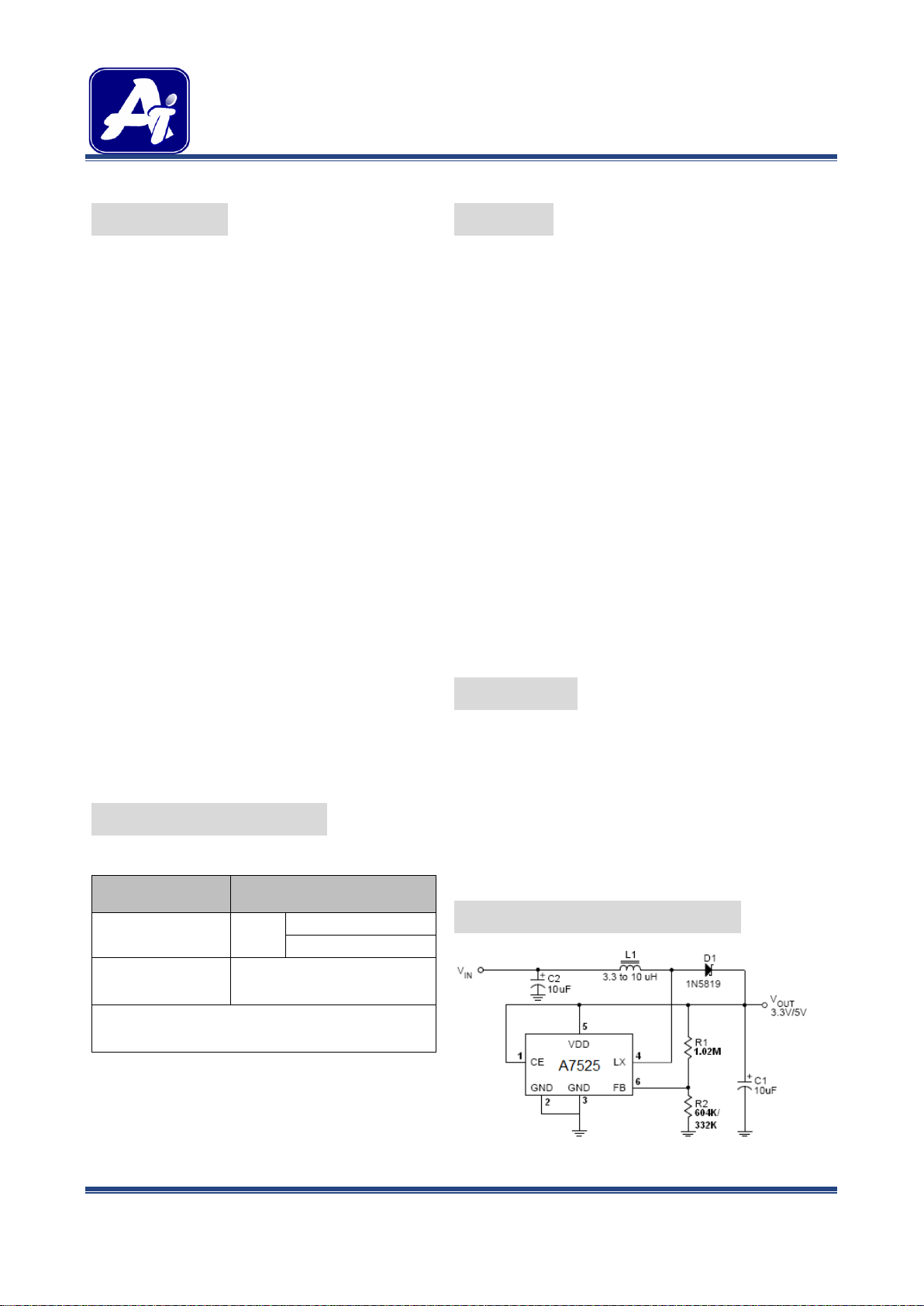
TYPICAL APPLICATION CIRCUIT
ORDERING INFORMATION
Package Type
Part Number
SOT-26
E6
A7525E6R-ADJ
A7525E6VR-ADJ
Note
V: Halogen free Package
R : Tape & Reel
AiT provides all RoHS products
Suffix “ V “ means Halogen free Package
REV1.0 - JAN 2012 RELEASE - - 1 -
Page 2

AiT Semiconductor Inc.
www.ait-ic.com
A7525
500mA, 1.2MHz HIGH EFFICIENCY
SYNCHRONOUS STEP-UP DC-DC CONVERTER
PIN DESCRIPTION
Top View
Pin #
Symbol
Function
1
CE
Chip Shutdown Signal Input. Logic high is normal operation mode, Logic Low is Shutdown
2,3
GND
Ground 4 LX
Power Switch Pin. It is the switch node connection to Inductor
5
VDD
Power Output Pin
6
FB
Feedback Input Pin. Connect FB to the center point of the external resistor divider.
The feedback threshold voltage is 1.23V
REV1.0 - JAN 2012 RELEASE - - 2 -
Page 3

AiT Semiconductor Inc.
www.ait-ic.com
A7525
500mA, 1.2MHz HIGH EFFICIENCY
SYNCHRONOUS STEP-UP DC-DC CONVERTER
ABSOLUTE MAXIMUM RATINGS
Input Voltage
-0.3V~+6V
FB, CE Voltage
-0.3V~+6V
VDD Voltage
-0.3V~+6V
Operating Temperature, T
OPR
NOTE1
-40℃~+85℃
Storage Temperature Range
-65℃~+150℃
Lead Temperature (Soldering, 10sec)
+300℃
Package
θJA
θJC
SOT-26
250℃/W
110℃/W
Stresses above may cause permanent damage to the device. These are stress ratings only and functional operation of the device at
these or any other conditions beyond those indicated in the Electrical Characteristics are not implied. Exposure to absolute maximum
rating conditions for extended periods may affect device reliability.
NOTE1: TJ is calculated from the ambient temperature TA and power dissipation PD according to the following formula:
TJ = TA + (PD) x (250°C/W)
THERMAL RESISTANCE
REV1.0 - JAN 2012 RELEASE - - 3 -
Page 4
AiT Semiconductor Inc.
www.ait-ic.com
A7525
500mA, 1.2MHz HIGH EFFICIENCY
SYNCHRONOUS STEP-UP DC-DC CONVERTER
ELECTRICAL CHARACTERISTICS
Parameter
Condition
Min.
Typ.
Max.
Unit
Minimum Start-Up Voltage
I
OUT
=1mA
- 1 -
V
Minimum Operating Voltage
VCE = VIN
-
0.8 - V
Output Voltage Range
2.5 - 5
V
Feedback Voltage
-40 ℃≤TA≤ 85℃
1.192
1.230
1.268
V
Quiescent Current(Shutdown)
V
SHDN
= 0V
0.01 1 μA
Quiescent Current(Active)
Measured on V
OUT
300
500
μA
NMOS Switch Leakage
VSW = 5V
-
0.1 5 μA
PMOS Switch Leakage
VSW = 0V
-
0.1 5 μA
NMOS Switch ON Resistance
V
OUT
= 3.3V
0.40 - Ω
V
OUT
= 5V
-
0.35 - Ω
PMOS Switch ON Resistance
V
OUT
= 3.3V
-
0.70 - Ω
V
OUT
= 5V
-
0.60 - Ω
Output Voltage
V
OUT
= 3.3V, I
OUT
= 1mA
3.201
3.300
3.399
V
V
OUT
= 5V , I
OUT
= 1mA,
VIN = 2.4V
4.850
5.000
5.150
V
Line Regulation
V
IN
= 0.8V to 3.0V,
I
OUT
= 10mA
- 1 -
%/V
Load Regulation
I
OUT
= 1mA to 100mA
-
0.02
-
%/mA
NMOS Current Limit
600
850 - mA
Current Limit Delay to Output
Note 2
-
40 - ns
Max Duty Cycle
VFB = 1.15V,
-40℃ ≤TA≤ 85℃
80
85 - %
Switching Frequency
0.95
1.2
1.5
MHz
-40℃ ≤TA ≤85℃
0.85
1.2
1.5
MHz
CE Input Threshold
0.35
0.60
1.50
V
CE Input Current
VCE = 5.5V
0.01 1 μA
VIN =1.2V, V
=3.3V, TA=25°C, unless otherwise specified
OUT
NOTE2: Guaranteed by design
REV1.0 - JAN 2012 RELEASE - - 4 -
Page 5
AiT Semiconductor Inc.
www.ait-ic.com
A7525
500mA, 1.2MHz HIGH EFFICIENCY
SYNCHRONOUS STEP-UP DC-DC CONVERTER
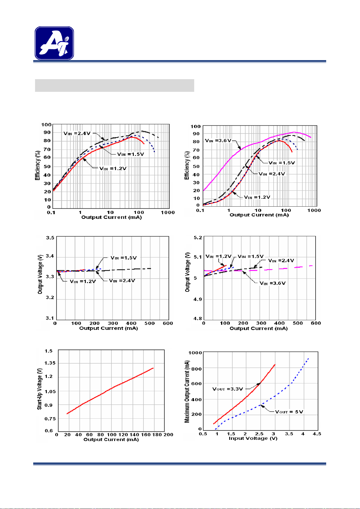
TYPICAL PERFORMANCE CHARACTERISTICS
1. Efficiency vs. Output Current
V
OUT
=3.3V, TA = 25°C
2. Input current vs. Output current
V
OUT
=5.0V, TA = 25°C
3. Output Voltage vs. Output Current
V
OUT
=3.3V, TA = 25°C
4. Output Voltage vs. Output Current
V
OUT
=5.0V, TA = 25°C
5. Minimum Start-Up Voltage vs. Output Current
V
OUT
=3.3V, TA = 25°C
6. Maximum Output Current vs. Input Voltage
L=4.7uH, TA = 25°C
REV1.0 - JAN 2012 RELEASE - - 5 -
Page 6

AiT Semiconductor Inc.
www.ait-ic.com
A7525
500mA, 1.2MHz HIGH EFFICIENCY
SYNCHRONOUS STEP-UP DC-DC CONVERTER
7. No Load Input Current vs. Input Voltage
V
OUT
=3.3V, TA = 25°C, No Load
8. V
OUT
vs. Temperature
9. Pulse Skipping Mode operation
10. Antiringing Operation at SW
11. Load Transient Response
REV1.0 - JAN 2012 RELEASE - - 6 -
Page 7

AiT Semiconductor Inc.
www.ait-ic.com
A7525
500mA, 1.2MHz HIGH EFFICIENCY
SYNCHRONOUS STEP-UP DC-DC CONVERTER
BLOCK DIAGRAM
REV1.0 - JAN 2012 RELEASE - - 7 -
Page 8

AiT Semiconductor Inc.
www.ait-ic.com
A7525
500mA, 1.2MHz HIGH EFFICIENCY
SYNCHRONOUS STEP-UP DC-DC CONVERTER
DEATAILED INFORMATION
Operation
The A7525 is 1.2MHz, synchronous boost converter housed in SOT-26 package. Able to operate from an
input voltage 1V, the device features fixed frequency, current mode PWM control for exceptional line and load
regulation. With its low RDS (ON) and gate charge internal MOSFET switches, the device maintains high
efficiency over a wide range of load current. Detailed descriptions of the operating modes follow. Operation
can be best understood by referring to the Block Diagram.
Synchronous Rectification
The A7525 integrates a synchronous rectifier to improve efficiency as well as to eliminate the external
Schottky diode. The synchronous rectifier is used to reduce the conduction loss contributed by the forward
voltage of Schottky diode. The synchronous rectifier is realized by a P-ch MOSFET with gate control circuitry
that incorporates relatively complicated timing concerns.
Low Voltage Start-Up
The A7525 will start up at a typical VIN of 1.0V or higher. The low voltage start-up circuitry controls the internal
NMOS switch up to a maximum peak inductor current of 850mA (typical), with an approximate1.5us off-time
during start-up, allowing the devices to start up into an output load. Once V
exceeds 2.3V, the start-up
OUT
circuitry is disabled and normal fixed frequency PWM operation is initiated. In this mode, the A7525 operate
allowing extended operating time as the battery can droop to several tenths of a volt without affecting output
voltage regulation. The limiting factor for the application becomes the ability of the battery to supply sufficient
energy to the output.
Low Noise Fixed Frequency Operation
Oscillator: The frequency of operation is internally set to 1.2MHz. Error Amp: The error amplifier is an
internally compensated trans-conductance type (current output) with a trans-conductance (gm) = 33
micro-siemens. The internal 1.23V reference voltage is compared to the voltage at the FB pin to generate an
error signal at the output of the error amplifier. A voltage divider from V
to ground programs the output
OUT
voltage via FB from 2.5V to 5V using the equation:
REV1.0 - JAN 2012 RELEASE - - 8 -
V
= 1.23V x [1 + (R1/R2)]
OUT
Page 9

AiT Semiconductor Inc.
www.ait-ic.com
A7525
500mA, 1.2MHz HIGH EFFICIENCY
SYNCHRONOUS STEP-UP DC-DC CONVERTER
Current Sensing: A signal representing NMOS switch current is summed with the slope compensator.
V
OUT
R1(Ω)
R2(Ω)
3.3V
1.02M
604K
5.0V
1.02M
332K
The summed signal is compared to the error amplifier output to provide a peak current control command for
the PWM. Peak switch current is limited to approximately 850mAindependent of input or output voltage. The
current signal is blanked for 40ns to enhance noise rejection.
Zero Current Comparator: The zero current comparator monitors the inductor current to the output and shuts
off the synchronous rectifier once this current reduces to approximately 20mA. This prevents the inductor
current from reversing in polarity improving efficiency at light loads.
Antiringing Control: The antiringing control circuitry pre-vents high frequency ringing of the LX pin as the
inductor current goes to zero by damping the resonant circuit formed by L and CLX (capacitance on LX pin).
Pulse Skipping Mode
At very light load, the A7525 automatically switches into Pulse Skipping Mode to improve efficiency. During
this mode, the PWM control will skip some pulses to maintain regulation. If the load increases and the output
voltage drops, the device will automatically switch back to normal PWM mode and maintain regulation.
Device Shutdown
When CE is set logic high, the A7525 is put into operation. If CE is set logic low, the device is put into
shutdown mode and consumes lower than 1μA current. After start-up timing, the internal circuitry is supplied
by V
, however, if shutdown mode is enabled, the internal circuitry will be supplied by battery again.
OUT
Application
Setting the Output Voltage: An external resistor divider is used to set the output voltage. The output voltage of
the switching regulator (V
) is determined by the following equation:
OUT
V
= 1.23V x [1 + (R1/R2)]
OUT
Table 1 list the resistor selection for output voltage setting.
Table 1 Resistor selection for output voltage setting
REV1.0 - JAN 2012 RELEASE - - 9 -
Page 10

AiT Semiconductor Inc.
www.ait-ic.com
A7525
500mA, 1.2MHz HIGH EFFICIENCY
SYNCHRONOUS STEP-UP DC-DC CONVERTER
Inductor Selection: The high switching frequency of 1.2MHz allows for small surface mount inductors. For
I
OUT
= η x
[
I
PEAK
-
V
IN
x D
]
x (1-D)
2 x
f
x L
Part Number
L(μH)
Max DCR (mΩ)
Rated D.C. Current (A)
Size WxLxH (mm)
Sumida
CR43
4.7
10
108.7
182
1.15
1.04
4.3x4.8x3.5
Sumida
CDRH4D28
4.7
5.6
6.8
10
72
101
109
128
1.32
1.17
1.12
1.00
5.0x5.0x3.0
Toko
D53LC
4.7
6.8
10
45
68
90
1.87
1.51
1.33
5.0x5.0x3.0
most designs, the A7525 operates with inductors of 4.7μH to 10μH.The equation below can help to select the
inductor, the maximum output current can be get by this equation; where η is the efficiency, I
current limit, f is the switching frequency, L is the inductance value and D is the duty cycle.
Larger inductors mean less inductor current ripple and usually less output voltage ripple. Larger inductors also
mean more load power can be delivered. But large inductors are also with large profile and costly. The
inductor ripple current is typically set for 20% to 40% of the maximum inductor current. When selecting an
inductor, the DC current rating must be high enough to avoid saturation at peak current. For optimum load
transient and efficiency, the low DCR should be selected. Table 2 lists some typical surface mount inductors
that meet target applications for the A7525:
Table2. Typical Surface Mount Inductors
is the peak
PEAK
Output Capacitor Selection: The output capacitor is required to keep the output voltage ripple small and to
ensure regulation loop stability. A 2.2μF to 10μF output capacitor is sufficient for most applications. If output
capacitor is larger than 10μF, a phase lead capacitor must be included to maintain enough phase margin. The
output capacitor must have low impedance at the switching frequency. Ceramic capacitors with X5R or X7R
dielectrics are recommended due to their low ESR and high ripple current ratings.
REV1.0 - JAN 2012 RELEASE - - 10 -
Page 11

AiT Semiconductor Inc.
www.ait-ic.com
A7525
500mA, 1.2MHz HIGH EFFICIENCY
SYNCHRONOUS STEP-UP DC-DC CONVERTER
Input Capacitor Selection: The input capacitor reduces the surge current drawn from the input and switching
noise from the device. A minimum 4.7μF input capacitor is needed for most applications. The input capacitor
impedance at the switching frequency should be less than input source impedance to prevent high frequency
switching current passing to the input. A low ESR input capacitor sized for maximum RMS current must be
used. Ceramic capacitors with X5R or X7R dielectrics are highly recommended because of their low ESR and
small temperature coefficients.
Output Diode Selection: An Shottky diode should be included when the output voltage is above 4.5V. The
Schottky diode is optional for the output voltage not more than 4.5V, but can improve efficiency by about 2%
to 3%.
PCB Layout Guidance
The A7525 operates at 1.2MHz typically. This is a considerably high frequency for DC-DC converters. In such
case PCB layout is important to guarantee satisfactory performance. It is recommended to make traces of the
power loop, especially where switching node is involved as short and wide as possible. First of all, the
inductor, input and output capacitor should be close to the device. Feedback and shut down circuit should
avoid the proximity of large AC signals, e.g. the power inductor and switching nodes. The optional rectifier
diode (D1) can improve efficiency and alleviate the stress on the integrated MOSFET. The diode should also
be close to the inductor and the chip to form the shortest possible switching loop. Large and integral multi
layer ground planes are ideal for high power applications. Large area of copper has lower resistance and
helps to dissipate heat on the device. The converter’s ground should join the system ground to which it
supplies power at one point only.
REV1.0 - JAN 2012 RELEASE - - 11 -
Page 12

AiT Semiconductor Inc.
www.ait-ic.com
A7525
500mA, 1.2MHz HIGH EFFICIENCY
SYNCHRONOUS STEP-UP DC-DC CONVERTER
PACKAGING INFORMATION
SYMBOL
MIN
MAX
A
1.100
1.300
A1
0.010
0.130
A2
1.000
1.170
b
0.300
0.500
c
0.090
0.200
D
2.800
3.100
E
1.500
1.700
E1
2.500
3.100
e
0.950(RFE)
e1
1.900(RFE)
L
0.350
0.800
θ
0°
10°
Dimension in SOT-26 (Unit: mm)
REV1.0 - JAN 2012 RELEASE - - 12 -
Page 13

AiT Semiconductor Inc.
www.ait-ic.com
A7525
500mA, 1.2MHz HIGH EFFICIENCY
SYNCHRONOUS STEP-UP DC-DC CONVERTER
IMPORTANT NOTICE
AiT Semiconductor Inc. (AiT) reserves the right to make changes to any its product, specifications, to
discontinue any integrated circuit product or service without notice, and advises its customers to obtain the
latest version of relevant information to verify, before placing orders, that the information being relied on is
current.
AiT Semiconductor Inc.'s integrated circuit products are not designed, intended, authorized, or warranted to
be suitable for use in life support applications, devices or systems or other critical applications. Use of AiT
products in such applications is understood to be fully at the risk of the customer. As used herein may
involve potential risks of death, personal injury, or servere property, or environmental damage. In order to
minimize risks associated with the customer's applications, the customer should provide adequate design and
operating safeguards.
AiT Semiconductor Inc. assumes to no liability to customer product design or application support. AiT
warrants the performance of its products of the specifications applicable at the time of sale.
REV1.0 - JAN 2012 RELEASE - - 13 -
Page 14

 Loading...