

Page 1
AiT Semiconductor Inc.
www.ait-ic.com
A7404
DC-DC CONVERTER/BUCK (STEP-DOWN)
42V INPUT STANDOFF VOLTAGE, 0.4A STEP-DOWN CONVERTER
DESCRIPTION
FEATURES
The A7404 is a wide input range, high-efficiency, and
high frequency DC-to-DC step-down switching
regulator, capable of delivering up to 0.4A of output
current. With a fixed switching frequency of 750kHz,
this current mode PWM controlled converter allows
the use of small external components, such as
ceramic input and output caps, as well as small
inductors. A7404 also employs a proprietary control
scheme that switches the device into a power save
mode during light load, thereby extending the range
of high efficiency operation. An OVP function protects
the IC itself and its downstream system against input
voltage surges. With this OVP function, the IC can
stand off input voltage as high as 42V, making it an
ideal solution for industrial applications such as smart
meters as well as automotive applications.
In automotive systems, power comes from the
battery, with its voltage typically between 9V and 24V.
Including cold crank and double battery jump-starts,
the minimum input voltage may be as low as 4V and
the maximum up to 36V, with even higher transient
voltages. With these high input voltages, linear
regulators cannot be used for high supply currents
without overheating the regulator. Instead, high
efficiency switching regulators such as A7404 must
be used to minimize thermal dissipation.
The A7404 is available in SOT-26 package.
ORDERING INFORMATION
Package Type
Part Number
SOT-26
E6
A7404E6R
A7404E6VR
Note
V: Halogen free Package
R: Tape & Reel
AiT provides all RoHS products
Suffix “ V “ means Halogen free Package
Wide Input Operating Range from 4V to 38V
Standoff Input Voltage: 42V
High Efficiency at 20V In 12V Out Up to 95%
High Efficiency PFM mode at light load
Capable of Delivering 0.4A of output current.
No External Compensation Needed
Current Mode control
Logic Control Shutdown
Thermal shutdown and UVLO
Available in SOT-26 Package
APPLICATION
Smart Meters
Industrial Applications
Automotive Applications
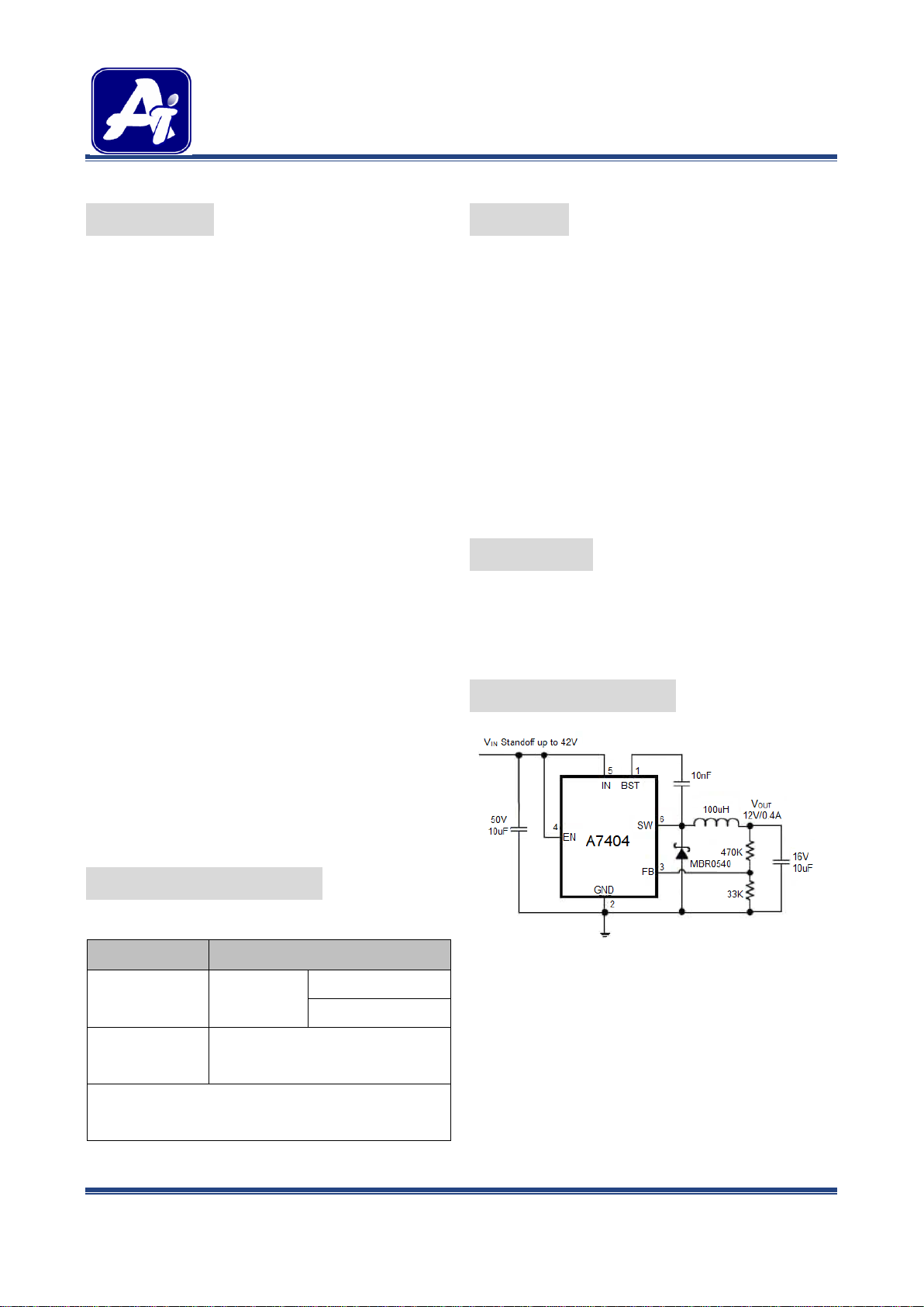
TYPICAL APPLICATION
REV1.0 - DEC 2015 RELEASED - - 1 -
Page 2

AiT Semiconductor Inc.
www.ait-ic.com
A7404
DC-DC CONVERTER/BUCK (STEP-DOWN)
42V INPUT STANDOFF VOLTAGE, 0.4A STEP-DOWN CONVERTER
PIN DESCRIPTION
Top View
Pin #
Symbol
Function
1
BST
Bootstrap pin. Connect a 10nF capacitor from this pin to SW
2
GND
Ground
3
FB
Feedback Input. Connect an external resistor divider from the output to FB and
GND to set V
OUT
4
EN
Enable pin for the IC. Drive this pin high to enable the part, low to disable.
5
IN
Supply Voltage. Bypass with a 10μF ceramic capacitor to GND
6
SW
Inductor Connection. Connect an inductor Between SW and the regulator output.
REV1.0 - DEC 2015 RELEASED - - 2 -
Page 3
AiT Semiconductor Inc.
www.ait-ic.com
A7404
DC-DC CONVERTER/BUCK (STEP-DOWN)
42V INPUT STANDOFF VOLTAGE, 0.4A STEP-DOWN CONVERTER
ABSOLUTE MAXIMUM RATINGS
Input Voltage Range
-0.3V~42V
TJ, Max Operating Junction Temperature
150°C
SW, EN Voltage
-0.3V~VIN+0.3V
BST Voltage
-0.3V~SW+6V
FB Voltage
-0.3V~6V
SW to ground current
Internally limited
TO, Operating Temperature
-40°C~85°C
θJC, Package Thermal Resistance
SOT-26
110°C/W
TS, Storage Temperature
-55°C~150°C
Parameter
Conditions
Min.
Typ.
Max.
Unit
Input Standoff Voltage
42
V
Input Voltage Range
4
38
V
Input UVLO
Rising, Hysteresis=140mV
3.80 V
Input OVP
Rising, Hysteresis=1.3V
38 V
Input Supply Current
VFB=0.85V
0.6 mA
Input Shutdown Current
6 μA
FB Feedback Voltage
0.780
0.800
0.820
V
FB Input Current
0.01 μA
Switching Frequency
750
kHz
Maximum Duty Cycle
90 % FoldBack Frequency
VFB=0V
95 kHz
High side Switch On Resistance
ISW=200mA
550 mΩ
High side Switch Current Limit
0.7 A
SW Leakage Current
VIN=12V, VSW=0, EN=GND
10
μA
EN Input Current
VIN=12V, VEN=5V
1 5
μA
EN Input Low Voltage
Rising, Hysteresis=100mV
0.8
1.1
1.4
V
Thermal Shutdown
Hysteresis=40°C
150 °C
Stress beyond above listed “Absolute Maximum Ratings” may lead permanent damage to the device. These are stress ratings only and
operations of the device at these or any other conditions beyond those indicated in the operational sections of the specifications are not
implied. Exposure to absolute maximum rating conditions for extended periods may affect device reliability.
ELECTRICAL CHARACTERISTICS
VIN=12V, unless otherwise specified. Typical values are at TA=25°C.
REV1.0 - DEC 2015 RELEASED - - 3 -
Page 4

AiT Semiconductor Inc.
www.ait-ic.com
A7404
DC-DC CONVERTER/BUCK (STEP-DOWN)
42V INPUT STANDOFF VOLTAGE, 0.4A STEP-DOWN CONVERTER
TYPICAL PERFORMANCE CHARACTERISTICS
1. Efficiency vs. I
OUT
2. Output Voltage vs. I
OUT
3. Frequency vs. Temperature
4. Maximum I
OUT
vs. Temperature
5. Efficiency vs. I
OUT
6. Output Voltage vs. I
OUT
Typical values are at TA=25°C, unless otherwise specified.
REV1.0 - DEC 2015 RELEASED - - 4 -
Page 5

AiT Semiconductor Inc.
www.ait-ic.com
A7404
DC-DC CONVERTER/BUCK (STEP-DOWN)
42V INPUT STANDOFF VOLTAGE, 0.4A STEP-DOWN CONVERTER
7. Efficiency vs. I
OUT
8. Output Voltage vs. I
OUT
9. Switching Forms: V
IN
=12V,V
OUT
=5V,I
OUT
=10mA
10. Switching Forms : V
IN
=12V,V
OUT
=5V,I
OUT
=25mA
11. Switching Forms: V
IN
=20V,V
OUT
=12V,I
OUT
=5mA
12. Switching Forms:V
IN
=20V,V
OUT
=12V,I
OUT
=30mA
13. Output Short Response V
IN
=36V,V
OUT
=12V
14. Output Short Recover V
IN
=36V,V
OUT
=12V
REV1.0 - DEC 2015 RELEASED - - 5 -
Page 6

AiT Semiconductor Inc.
www.ait-ic.com
A7404
DC-DC CONVERTER/BUCK (STEP-DOWN)
42V INPUT STANDOFF VOLTAGE, 0.4A STEP-DOWN CONVERTER
BLOCK DIAGRAM
REV1.0 - DEC 2015 RELEASED - - 6 -
Page 7

AiT Semiconductor Inc.
www.ait-ic.com
A7404
DC-DC CONVERTER/BUCK (STEP-DOWN)
42V INPUT STANDOFF VOLTAGE, 0.4A STEP-DOWN CONVERTER
DETAILED INFORMATION
Functional Descriptions
Loop Operation
The A7404 is a wide input range, high-efficiency, DC-to-DC step-down switching regulator, capable of
delivering up to 0.4A of output current, integrated with a 550mΩ high side MOSFET. It uses a PWM
current-mode control scheme. An error amplifier integrates error between the FB signal and the internal
reference voltage. The output of the integrator is then compared to the sum of a current-sense signal and the
slope compensation ramp. This operation generates a PWM signal that modulates the duty cycle of the power
MOSFETs to achieve regulation for output voltage.
Light Load Operation
Traditionally, a fixed constant frequency PWM DC-DC regulator always switches even when the output load is
small. When energy is shuffling back and forth through the power MOSFETs, power is lost due to the finite
RDSONs of the MOSFETs and parasitic capacitances. At light load, this loss is prominent and efficiency is
therefore very low. A7404 employs a proprietary control scheme that improves efficiency in this situation by
enabling the device into a power save mode during light load, thereby extending the range of high efficiency
operation.
REV1.0 - DEC 2015 RELEASED - - 7 -
Page 8

AiT Semiconductor Inc.
www.ait-ic.com
A7404
DC-DC CONVERTER/BUCK (STEP-DOWN)
42V INPUT STANDOFF VOLTAGE, 0.4A STEP-DOWN CONVERTER
PACKAGE INFORMATION
SYMBOL
MIN
MAX
A
1.050
1.250
A1
0.000
0.100
A2
1.050
1.150
b
0.300
0.500
c
0.100
0.200
D
2.820
3.020
E
1.500
1.700
E1
2.650
2.950 e 0.950(BSC)
e1
1.800
2.000
L
0.300
0.600
θ
0°
8°
Dimension in SOT-26 Package (Unit: mm)
REV1.0 - DEC 2015 RELEASED - - 8 -
Page 9

AiT Semiconductor Inc.
www.ait-ic.com
A7404
DC-DC CONVERTER/BUCK (STEP-DOWN)
42V INPUT STANDOFF VOLTAGE, 0.4A STEP-DOWN CONVERTER
IMPORTANT NOTICE
AiT Semiconductor Inc. (AiT) reserves the right to make changes to any its product, specifications, to
discontinue any integrated circuit product or service without notice, and advises its customers to obtain the
latest version of relevant information to verify, before placing orders, that the information being relied on is
current.
AiT Semiconductor Inc.'s integrated circuit products are not designed, intended, authorized, or warranted to
be suitable for use in life support applications, devices or systems or other critical applications. Use of AiT
products in such applications is understood to be fully at the risk of the customer. As used herein may involve
potential risks of death, personal injury, or servere property, or environmental damage. In order to minimize
risks associated with the customer's applications, the customer should provide adequate design and
operating safeguards.
AiT Semiconductor Inc. assumes to no liability to customer product design or application support. AiT
warrants the performance of its products of the specifications applicable at the time of sale.
REV1.0 - DEC 2015 RELEASED - - 9 -
Page 10

 Loading...