

Page 1
Philips Semiconductors Product specification
µA723/723CPrecision voltage regulator
1
1994 Aug 31 853-1063 13721
DESCRIPTION
The µA723/µA723C is a monolithic precision voltage regulator
capable of operation in positive or negative supplies as a series,
shunt, switching, or floating regulator. The 723 contains a
temperature-compensated reference amplifier, error amplifier, series
pass transistor, and current limiter, with access to remote shutdown.
FEATURES
•Positive or negative supply operation
•Series, shunt, switching, or floating operation
•0.01% line and load regulation
•Output voltage adjustable from 2V to 37V
•Output current to 150mA without external pass transistor
•µA723 MIL-STD-883A, B, C available
PIN CONFIGURATION
D,F, N Packages
1
2
3
4
5
6
7 8
14
13
12
11
10
9
NC
CURRENT LIMIT
CURRENT SENSE
INVERTING INPUT
NON-INVERTING INPUT
V–
V
REF
NC
FREQUENCY COMPENS.
NC
V+
V
C
V
OUT
V
Z
SL00503
Figure 1. Pin Configuration
ORDERING INFORMATION
DESCRIPTION TEMPERATURE RANGE ORDER CODE DWG #
14-Pin Ceramic Dual In-Line Package (CERDIP) -55°C to 125°C µA723F 0581B
14-Pin Plastic Dual In-Line Package (DIP) 0 to 70°C µA723CN SOT27-1
14-Pin Plastic Small Outline (SO) Package 0 to 70°C µA723CD SOT108-1
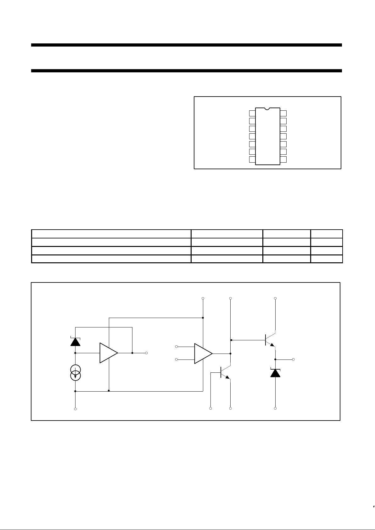
EQUIVALENT CIRCUIT
TEMPERATURE
COMPENSATED
ZENER
7
V–
VOLTAGE
REFERENCE
AMPLIFIER
INVERTING
INPUT
4
ERROR AMP
NON INVERTING
INPUT
–
+
CURRENT
LIMIT
2
3
CURRENT
SENSE
FREQUENCY
COMPENSATION
V+
12
13 11
SERIES PASS
TRANSISTOR
10
9
V
C
V
Z
V
OUT
8
V
REF
V
IN
SL00504
Figure 2. Equivalent Circuit
Page 2

Philips Semiconductors Product specification
µA723/723CPrecision voltage regulator
1994 Aug 31
2
ABSOLUTE MAXIMUM RATINGS
SYMBOL PARAMETER RATING UNIT
Pulse voltage from V+ to V- (50ms) 50 V
Continuous voltage from V+ to V- 40 V
Input-output voltage differential 40 V
V
DIFF
Error amplifier maximum input differential voltage ±5 V
V
CM
Error amplifier non-inverting input (Pin 5) to -V (Pin 7) 8 V
I
OUT
Maximum output current 150 mA
Current from V
REF
15 mA
Current from V
Z
25 mA
P
MAX
Maximum power dissipation TA=25°C (still-air)
1
F package 1190 mW
N package 1420 mW
D package 1040 mW
T
A
Operating ambient temperature range
µA723
µA723C
-55 to +125
0 to 70
°C
°C
T
STG
Storage temperature range -65 to +150 °C
T
SOLD
Lead soldering temperature (10sec max) 300 °C
NOTES:
1. The following derating factors should be applied above 25°C
F package at 9.5mW/°C
N package at 11.4mW/°C
D package at 8.3mW/°C
Page 3

Philips Semiconductors Product specification
µA723/723CPrecision voltage regulator
1994 Aug 31
3
DC ELECTRICAL CHARACTERISTICS
TA=25°C, unless otherwise specified.
1
µA723 µA723C
SYMBOL
PARAMETER
TEST CONDITIONS
Min Typ Max Min Typ Max
UNITS
VIN=12V to VIN=15V 0.01 0.1 0.01 0.1
V
R LINE
Line regulation
2
VIN=12V to VIN=40V 0.02 0.2 0.1 0.5
%V
OUT
V
R LOAD
Load regulation
2
IL=1mA to IL=50mA 0.03 0.15 0.03 0.2 %V
OUT
f=50Hz to 10kHz, C
REF
=0 74 74
∆VIN/∆ VO
Ripple Rejection
f=50Hz to 10kHz, C
REF
=5µF 86 86
dB
I
OS
Short-circuit current RSC=10Ω, V
OUT
=0 65 65 mA
V
REF
Reference voltage I
REF
=0.1mA 6.95 7.15 7.35 6.80 7.15 7.50 V
V
REF (LOAD)
Reference voltage
change with load
I
REF
=0.1mA to 5mA 20 20 mV
BW=100Hz to 10kHz, C
REF
=0 20 20
V
NOISE
Output noise voltage
BW=100Hz to 10kHz, C
REF
=5µF 2.5 2.5
µV
RMS
S Long-term stability Tj=Tjmax.
TA=25°C for end point
measurment
0.1 0.1 %1000 hrs.
I
SCD
Standby current drain IL=0, VIN=30V 2.3 3.5 2.3 4.0 mA
V
IN
Input voltage range 9.5 40 9.5 40 V
V
OUT
Output voltage range 2.0 37 2.0 37 V
V
DIFF
Input-output voltage
differential
3.0 38 3.0 38 V
The following specifications apply over the operating temperature ranges.
V
R LINE
Line regulation VIN=12V to VIN=15V 0.3 0.3 %V
OUT
V
R LOAD
Load regulation IL=1mA to IL=50mA 0.6 0.6 %V
OUT
TC
Average temperature
coefficient of output
voltage
0.002 0.015 0.003 0.015 %/°C
NOTES:
1. V
IN
=V+=VC=12V, V-=0V, V
OUT
=5V, IL=1mA, RSC=0, C1=100pF, C
REF
=0 and divider impedance as seen by error amplifier≤10kΩ.
2. The load and line regulation specifications are for constant junction temperature. Temperature drift effects must be taken into account
separately when the unit is operating under conditions of high dissipation.
Page 4

Philips Semiconductors Product specification
µA723/723CPrecision voltage regulator
1994 Aug 31
4
TYPICAL PERFORMANCE CHARACTERISTICS
Standby Current Drain
as a Function of Input Voltage
Maximum Load Current
as a Function of
Input-Output Voltage
Differential
Load Regulation
Characteristics with
Current Limiting
Current Limiting
Characteristics as a
Function of Junction
Temperature
Maximum Load Current
as a Function of
Input-Output Voltage
Differential
Load Regulation
Characteristics Without
Current Limiting
Load Transient Response
Line Regulation as a
Function of Input-Output
Voltage Differential
Output Impedance as
a Function of Frequency
5.0
4.0
3.0
2.0
1.0
0
0 10 20 30 40 50
INPUT VOLTAGE — V
STANDBY CURRENT
TA = +70°C
TA = +125°C
V
OUT
= V
REF
IL = 0
TA = –55°C
T
A
= 0°C
T
A
= +25°C
0.8
0.7
0.6
0.5
0.4
0.3
–50 0 +50 +100 +150
200
160
120
80
40
0
CURRENT LIMIT SENSE VOLTAGE — V
JUNCTION TEMPERATURE — °C
SENSE VOLTAGE
LIMIT CURRENT
R
SC
= 10Ω
LIMIT CURRENT
R
SC
= 5Ω
200
TA = +25°C
T
A
= 70°C
T
A
= +125°C
160
120
80
40
0
T
JMAX
= 150°C
R
TH
= 150°C/W
P
STANDBY
= 60mW
METAL CAN PACKAGE
(NO HEAT SINK)
0 10 20 30 40 50
(VIN – V
OUT
) — V
I — mA
LMAX
200
160
120
80
40
0
0 10 20 30 40 50
I — mA
LMAX
TA = +25°C
T
A
= 70°C
T
A
= +125°C
T
JMAX
= 150°C
R
TH
= 111°C/W
P
STANDBY
= 60mW
DIP PACKAGE
(NO HEAT SINK)
(V
IN
– V
OUT
) — V
LIMITING CURRENT — mA
TA = –55°C
T
A
= +25°C
T
A
= +70°C
V
OUT
= 5V, VIN = +12V
R
SC
= 10Ω
TA = +125°C
TA = 0°C
+0.1
0
–0.1
–0.2
–0.3
–0.4
20 40 60 80 1000
OUTPUT CURRENT — mA
REGULATION — % V
OUT
+0.05
0
–0.05
–0.1
–0.15
–0.2
0
20 40
60 80 100
OUTPUT CURRENT — mA
TA = 70°C
T
A
= +25°C
T
A
= 0°C
T
A
= +125°C
T
A
= +55°C
V
OUT
= 5V
R
SC
= 0
VIN = +12V
REGULATION — % V
OUT
+0.3
+0.2
+0.1
0
–0.1
–0.2
–5 5 15 25 35 45
OUTPUT IMPEDANCE —
V
OUT
= +5V
R
SC
= 0
T
A
= +25°C
∆V
IN
= +3V
I
IL
= 1mA
REGULATION — % V
OUT
(VIN – V
OUT
) — V
V
OUT
= 5V
I
L
= 40mA
VIN = +12V
4.0
R
SC
= 0
0
–4.0
–8.0
–5 5 15 25 35 45
OUTPUT VOLTAGE
OUTPUT VOLTAGE DEVIATION — mV
LOAD CURRENT
+10
0
TIME — µs
10
1.0
0.1
.01
100
1k
10k
100k 1M
FREQUENCY — Hz
Ω
VO = +5V
R
SC
= 0
T
A
= +25°C
V
IN
= +12V
I
IL
= 50mA
C1 = 0
C1 = 1µF
LOAD DEVIATION – mA
SL00505
Figure 3. Typical Performance Characteristics
Page 5

Philips Semiconductors Product specification
µA723/723CPrecision voltage regulator
1994 Aug 31
5
TYPICAL PERFORMANCE CHARACTERISTICS (Continued)
(VIN – V
OUT
) — V
Line Transient Response
Load Regulation as a
Function of Input-Output
Voltage Differential
Current Limiting
Characteristics
4.0
2.0
0
OUTPUT VOLTAGE DEVIATION — mV
INPUT VOLTAGE
OUTPUT VOLTAGE
0
–2.0
–4.0
–5 5 15 25 35 45
–6.0
TIME — µs
+0.2
+0.1
0
0.1
–0.2
–0.3
REGULATION — %V
OUT
–5 5 2515 35 45
VO = +5V
R
SC
= 0
T
A
= +25°C
V
IN
= +12V
I
IL
= mA TO IL = 50mA
1.2
0
OUTPUT CURRENT — mA
OUTPUT VOLTAGE DEVIATION — V
1.0
0.8
0.6
0.4
0.2
0
20 40 60 80 100
TA = 0°C
TA = –55°C
T
A
= +25°C
T
A
= +70°C
T
A
= +125°C
VO = +5V
R
SC
= 10Ω
V
IN
= +12V
INPUT VOLTAGE DEVIATION – VOLTS
SL00506
Figure 4. Typical Performance Characteristics (cont.)
TYPICAL APPLICATIONS
NOTES:
V
OUT
V
REF
x
R
2
R1 R
2
R
3
R1R
2
R1 R
2
for minimum temperature drift
V
OUT
V
REF
2
x
R1 R
2
R
1
; R3 R
4
NOTE:
Low Voltage Regulator (V
OUT
= 2 to 7V) Negative Voltage Regulator
C
REF
R
2
R
1
COMP
V–
100pF
C
1
R
3
R
SC
V
C
V+
V
IN
REGULATED
OUTPUT
V
REF
V
OUT
CL
CS
INV
N.I.
V
REF
V
OUT
CL
CS
INV
N.I.
V
Z
R
4
R
3
COMP
100pF
C
1
REGULATED
OUTPUT
R
1
R
2
V+
V
C
R
5
T
1
SL00507
Figure 5. Typical Applications
Page 6

Philips Semiconductors Product specification
µA723/723CPrecision voltage regulator
1994 Aug 31
6
TYPICAL APPLICATIONS (Continued)
I
KNEE
V
OUT
R
3
RSCR
4
V
SENSE
(R3 R4)
RSCR
4
V
OUT
V
REF
X
R1 R
2
R
4
I
SHORT CKT
V
SENSE
R
SC
X
R3 R
4
R
4
R
4
R
3
V
OUTISC
V
SENSE
(I
KNEE
– I
SHORT CKT
)
– 1
R
SC
V
SENSE
I
SC
1
R
3
R
4
NOTES:
NOTES:
NOTE:
V
OUT
V
REF
x
R
2
R1 R
2
V
OUT
V
REF
x
R
2
R1 R
2
; R3 R
4
R
3
R1R
2
R1 R
2
for minimum temperature drift
NOTE:
R3 may be eliminated for minimum component count
Remote Shutdown Regulator With Current
Limiting (V
OUT
= 2 to 7V)
High Voltage Regulator (V
OUT
= 7 to 37V)
Foldback Current Limiting Regulator (V
OUT
= 2 to 7V)
R
2
R
4
COMP
V–
1nF
C
1
R
1
R
SC
V
C
V+
V
IN
V
REF
V
OUT
CL
CS
INV
N.I.
Q
1
R
3
2kΩ
2kΩ
LOGIC INPUT
REGULATED
OUTPUT
V
REF
V
OUT
CL
CS
INV
N.I.
V–
V+
V
IN
V
C
R
3
COMP
REGULATED
OUTPUT
R
2
R
1
100pF
C
1
R
SC
R
2
COMP
V–
R
1
V
C
V
IN
V
REF
V
OUT
CL
CS
INV
N.I.
R
SC
REGULATED
OUTPUT
1nF
C
1
R
4
R
3
V
Z
16
0
OUTPUT CURRENT — mA
OUTPUT VOLTAGE DEVIATION — V
R3 = 500Ω
R
SC
= 3.4Ω
R
4
= 3.6kΩ
14
12
10
8
6
4
2
0
I
SHORT
10 20 30 40 50 60
I
KNEE
SL00508
Figure 6. Typical Applications (cont.)
 Loading...