

Page 1
AiT Semiconductor Inc.
www.ait-ic.com
A7221
DESCRIPTION
FEATURES
ORDERING INFORMATION
Package Type
Part Number
APPLICATION
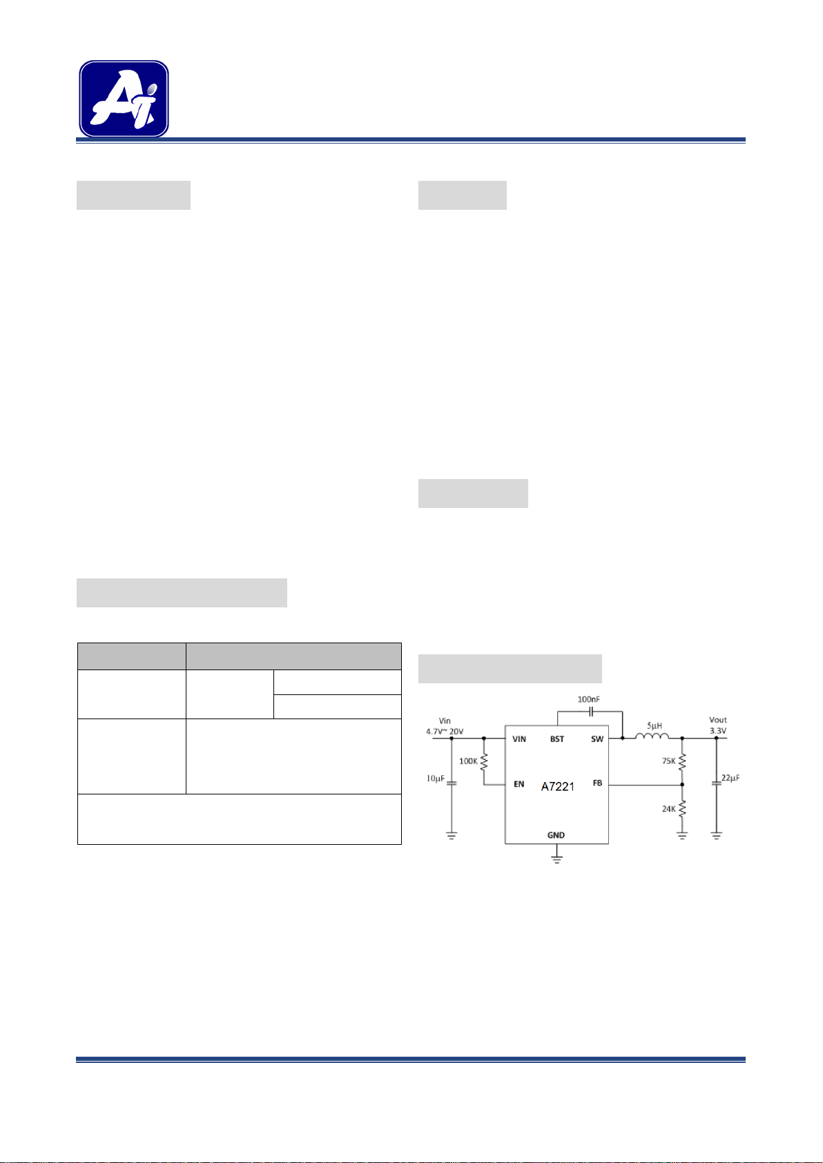
TYPICAL APPLICATION
DC-DC CONVERTER BUC K (STEP-DOWN)
2A, 20V SYNCHRONOUS
The A7221 is a current mode monolithic buck
voltage converter. Operating with an input range of
4.7V~20V, the A7221 delivers 2A of continuous
output current with two integrated N-Channel
MOSFETs. At light loads, regulators operate in low
frequency to maintain high efficiency and low output
ripple.
The A7221 guarantees robustness with over
current protection, thermal protection, start-up
current run-away protection, and input under
voltage lockout.
The A7221 is available in TSOT-26 package.
4.7V to 20V operating input range 2A output
current
Up to 95% efficiency
High efficiency (>80%) at light load
Fixed 500kHz Switching frequency
Input under voltage lockout
Start-up current run-away protection
Over current protection and Hiccup
Thermal protection
Available in TSOT-26 Package
Distributed Power Systems
Networking Systems
FPGA, DSP, ASIC Power Supplies
Green Electronics/ Appliances
Notebook Computers
TSOT-26 TE6
V: Halogen free Package
Note
R: Tape & Reel
SPQ:3,000pcs/Reel
AiT provides all RoHS products
Suffix “ V “ means Halogen free Package
REV3.0 - DEC 2013 RELEASED, MAR 2016 UPDATED - - 1 -
A7221TE6R
A7221TE6VR
2A Buck Voltage Converter
Page 2

AiT Semiconductor Inc.
www.ait-ic.com
A7221
Pin #
Symbol
Function
PIN DESCRIPTION
DC-DC CONVERTER BUC K (STEP-DOWN)
2A, 20V SYNCHRONOUS
Top View
1 GND Power ground pin.
SW is the switching node that supplies power to the output. Connect the
2 SW
output LC filter from SW to the output load.
supplies power to the IC. Connect a 4.7V to 20V
IN
3 VIN
Input voltage pin. V
supply to V
and bypass VIN to GND with a suitably large capacitor to
IN
eliminate noise on the input to the IC.
Output feedback pin. FB senses the output voltage and is regulated by
4 FB
the control loop to 0.8V. Connect a resistive divider at FB.
5 EN Drive EN pin high to turn on the regulator and low to turn off the regulator.
Boostrap pin for top switch. A 0.1uF or larger capacitor should be
6 BST
connected between this pin and the SW pin to supply current to the top
switch and top switch driver.
REV3.0 - DEC 2013 RELEASED, MAR 2016 UPDATED - - 2 -
Page 3
AiT Semiconductor Inc.
www.ait-ic.com
A7221
Parameter
Symbol
MIN
MAX
Units
Package
θJA
θJC
DC-DC CONVERTER BUC K (STEP-DOWN)
2A, 20V SYNCHRONOUS
ABSOLUTE MAXIMUM RATINGS
VIN, EN, SW PIN -0.3V~22V
BST PIN SW-0.3V~SW+5V
All other pins -0.3V~6V
Junction Temperature
NOTE1,2
150℃
Lead Temperature 260℃
Storage Temperature -65℃~+150℃
Stress beyond above listed “Absolute Maximum Ratings” may lead permanent damage to the device. These are stress ratings only and
operations of the device at these or any other conditions beyond those indicated in the operational sections of the specifications are not
implied. Exposure to absolute maximum rating conditions for extended periods may affect device reliability.
RECOMMENDED OPERATING CONDITIONS
Input Voltage VIN 4.7 20 V
Output voltage V
0.8 18 V
OUT
Junction Temperature TJ -40 125 ℃
THERMAL PERFORMANCE
NOTE3
TSOT-26 110℃/W 55℃/W
NOTE1: The A7221 guarantees robust performance from -40°C to 150°C junction temperature. The junction temperature range
specification is assured by design, characterization and correlation with statistical process controls.
NOTE2: The A7221 includes thermal protection that is intended to protect the device in overload conditions. Thermal protection is active
when junction temperature exceeds the maximum operating junction temperature. Continuous operation over the specified
absolute maximum operating junction temperature may damage the device.
NOTE3: Measured on JESD51-7, 4-layer PCB.
REV3.0 - DEC 2013 RELEASED, MAR 2016 UPDATED - - 3 -
Page 4

AiT Semiconductor Inc.
www.ait-ic.com
A7221
Parameter
Symbol
Conditions
Min.
Typ.
Max.
Unit
ELECTRICAL CHARACTERISTICS
=12V, TA=25℃, unless otherwise stated.
V
IN
DC-DC CONVERTER BUC K (STEP-DOWN)
2A, 20V SYNCHRONOUS
VIN Under voltage Lockout
V
VIN falling
IN_MIN
3.88 V
Threshold
VIN Under voltage Lockout
V
IN_MIN_HYST
360 mV
Hysteresis
Shutdown Supply Current ISD VEN=0V 1 μA
Supply Current IQ VEN=5V, VFB=2V 50 μA
Feedback Voltage VFB 776 800 824 mV
Top Switch Resistance R
Bottom Switch Resistance R
Top Switch Leakage Current I
Bottom Switch Leakage Current I
Top Switch Current Limit I
LEAK_TOP
LEAK_BOT
160 mΩ
DS(ON)T
80 mΩ
DS(ON)B
V
=20V, VEN=0V,
IN
V
=0V
SW
V
=20V, VEN=0V,
IN
V
=0V
SW
Minimum Duty Cycle 3.8 A
LIM_TOP
0.5 μA
0.5 μA
Switch Frequency FSW 500 kHz
Minimum On Time T
100 ns
ON_MIN
Minimum Off Time T
EN shut down threshold voltage V
EN shut down hysteresis V
Thermal Shutdown T
Temperature Hysteresis T
REV3.0 - DEC 2013 RELEASED, MAR 2016 UPDATED - - 4 -
OFF_MIN
EN_TH
EN_HYST
145 ℃
TSD
15 ℃
HYS
VFB=0.7V 100 ns
VEN falling, FB=0V 1.2 V
100 mV
Page 5

AiT Semiconductor Inc.
www.ait-ic.com
A7221
BLOCK DIAGRAM
DC-DC CONVERTER BUC K (STEP-DOWN)
2A, 20V SYNCHRONOUS
REV3.0 - DEC 2013 RELEASED, MAR 2016 UPDATED - - 5 -
Page 6

AiT Semiconductor Inc.
www.ait-ic.com
A7221
DC-DC CONVERTER BUC K (STEP-DOWN)
2A, 20V SYNCHRONOUS
DETAILED INFORMATION
FUNCTIONAL DESCRIPTION
The A7221 is a synchronous, buck voltage converter.
Current-Mode Control
The A7221 utilizes current-mode control to regulate the FB voltage. Voltage at the FB pin is regulated at 0.8V
so that by connecting an appropriate resistive divider between V
and GND, designed output voltage can be
OUT
achieved.
PFM Mode
The A7221 operates in PFM mode at light load. In PFM mode, switch frequency decreases when load current
drops to boost power efficiency at light load by reducing switch-loss, while switch frequency increases when
load current rises, minimizing output voltage ripples.
Internal Soft-Start
Soft-Start makes output voltage rising smoothly follow an internal SS voltage until SS voltage is higher than
the internal reference voltage. It can prevent overshoot of output voltage when startup.
Power Switch
N-Channel MOSFET switches are integrated on the A7221 to down convert the input voltage to the regulated
output voltage. Since the top MOSFET needs a gate voltage greater than the input voltage, a boost capacitor
connected between BST and SW pins is required to drive the gate of the top switch. The boost capacitor is
charged by the internal 3.3V rail when SW is low.
VIN Under-Voltage Protection
A resistive divider can be connected between VIN and GND, with the central tap connected to EN, so that
when V
drops to the pre-set value, EN drops below 1.2V to trigger input under voltage lockout protection.
IN
REV3.0 - DEC 2013 RELEASED, MAR 2016 UPDATED - - 6 -
Page 7

AiT Semiconductor Inc.
www.ait-ic.com
A7221
DC-DC CONVERTER BUC K (STEP-DOWN)
2A, 20V SYNCHRONOUS
Output Current Run-Away Protection
At start-up, due to the high voltage at input and low voltage at output, current inertia of the output inductance
can be easily built up, resulting in a large start-up output current. A valley current limit is designed in the
A7221 so that only when output current drops below the valley current limit can the top power switch be
turned on. By such control mechanism, the output current at start-up is well controlled.
Over Current Protection and Hiccup
A7221 has a cycle-by-cycle current limit. When the inductor current triggers current limit, A7221 enters hiccup
mode and periodically restart the chip.
A7221 will exit hiccup mode while not triggering current limit.
Thermal Protection
When the temperature of the A7221 rises above 145°C, it is forced into thermal shut-down.
Only when core temperature drops below 130°C can the regulator becomes active again.
REV3.0 - DEC 2013 RELEASED, MAR 2016 UPDATED - - 7 -
Page 8

AiT Semiconductor Inc.
www.ait-ic.com
A7221
PACKAGE INFORMATION
Dimension in TSOT-26 (Unit: mm)
DC-DC CONVERTER BUC K (STEP-DOWN)
2A, 20V SYNCHRONOUS
REV3.0 - DEC 2013 RELEASED, MAR 2016 UPDATED - - 8 -
Page 9

AiT Semiconductor Inc.
www.ait-ic.com
A7221
DC-DC CONVERTER BUC K (STEP-DOWN)
2A, 20V SYNCHRONOUS
IMPORTANT NOTICE
AiT Semiconductor Inc. (AiT) reserves the right to make changes to any its product, specifications, to
discontinue any integrated circuit product or service without notice, and advises its customers to obtain the
latest version of relevant information to verify, before placing orders, that the information being relied on is
current.
AiT Semiconductor Inc.'s integrated circuit products are not designed, intended, authorized, or warranted to
be suitable for use in life support applications, devices or systems or other critical applications. Use of AiT
products in such applications is understood to be fully at the risk of the customer. As used herein may involve
potential risks of death, personal injury, or servere property, or environmental damage. In order to minimize
risks associated with the customer's applications, the customer should provide adequate design and
operating safeguards.
AiT Semiconductor Inc. assumes to no liability to customer product design or application support. AiT
warrants the performance of its products of the specifications applicable at the time of sale.
REV3.0 - DEC 2013 RELEASED, MAR 2016 UPDATED - - 9 -
Page 10

 Loading...