

Page 1
AiT Semiconductor Inc.
www.ait-ic.com
A7221B
DC-DC CONVERTER BUCK (STEP-DOWN)
DESCRIPTION
FEATURES
ORDERING INFORMATION
Package Type
Part Number
A7221BE6R
A7221BE6VR
APPLICATION
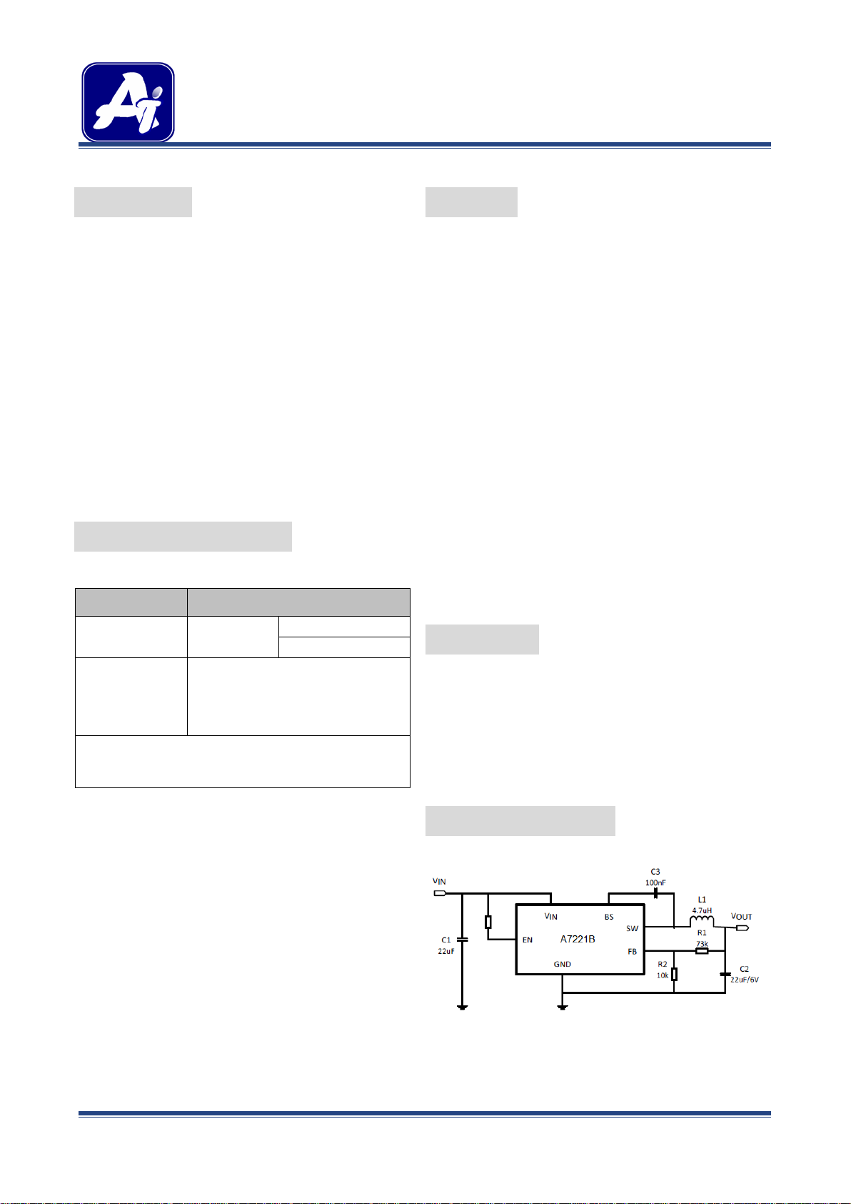
TYPICAL APPLICATION
2A 16V 600kHz SYNCHRONOUS
The A7221B is a fully integrated, high– efficiency 2A
synchronous rectified step-down converter. The
A7221B operates at high efficiency over a wide
output current load range.
This device offers two operation modes, PWM
control and PFM Mode switching control, which
allows a high efficiency over the wider range of the
load.
The A7221B is available in SOT-26 package.
SOT-26 E6
High Efficiency: Up to 96%
600kHz Frequency Operation
2A Output Current
No Schottky Diode Required
3.5V to 16V Input Voltage Range
0.6V Reference
Slope Compensated Current Mode Control for
Excellent Line and Load Transient Response
Integrated internal compensation
Stable with Low ESR Ceramic Output Capacitors
Over Current Protection with Hiccup-Mode
Thermal Shutdown
Inrush Current Limit and Soft Start
-40°C to +85°C Temperature Range
Available in SOT-26 Package
V: Halogen free Package
Note
AiT provides all RoHS products
Suffix “ V “ means Halogen free Package
R: Tape & Reel
SPQ:3,000pcs/Reel
Distributed Power Systems
Digital Set Top Boxes
Flat Panel Television and Monitors
Wireless and DSL Modems
Notebook Computer
REV1.0 - SEP 2016 RELEASED - - 1 -
Page 2
AiT Semiconductor Inc.
www.ait-ic.com
A7221B
DC-DC CONVERTER BUCK (STEP-DOWN)
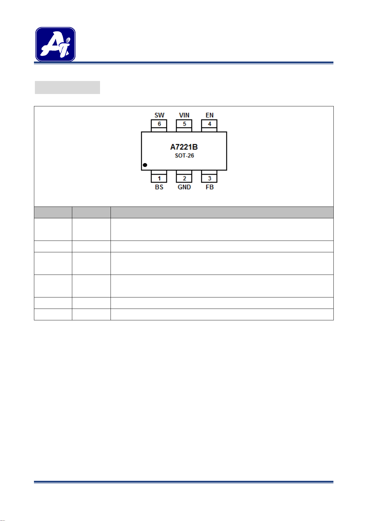
Pin #
Symbol
Function
to the center point of the
PIN DESCRIPTION
2A 16V 600kHz SYNCHRONOUS
Top View
1 BS
Bootstrap. A capacitor connected between SW and BS pins is required to form
a floating supply across the high-side switch driver.
2 GND Ground
Adjustable version feedback input. Connect FB
3 FB
external resistor divider.
Drive this pin to a logic-high to enable the IC. Drive to a logic-low to disable the
4 EN
IC and enter micro-power shutdown mode.
5 VIN Power supply Pin
6 SW Switching Pin
REV1.0 - SEP 2016 RELEASED - - 2 -
Page 3
AiT Semiconductor Inc.
www.ait-ic.com
A7221B
DC-DC CONVERTER BUCK (STEP-DOWN)
Parameter
Conditions
Min.
Typ.
Max.
Unit
2A 16V 600kHz SYNCHRONOUS
ABSOLUTE MAXIMUM RATINGS
VIN, Supply Voltage -0.3V ~ 25V
VSW, Switch Node Voltage -0.3V ~ (VIN+0.5V)
VBS, Boost Voltage VSW-0.3V ~ VSW+5V
All Other Pins -0.3V ~ 6V
Operating Temperature Range -40℃ ~ 85℃
Storage Temperature Range -65℃ ~ 150℃
Lead Temperature (Soldering,10s) 300℃
Stress beyond above listed “Absolute Maximum Ratings” may lead permanent damage to the device. These are stress ratings only and
operations of the device at these or any other conditions beyond those indicated in the operational sections of the specifications are not
implied. Exposure to absolute maximum rating conditions for extended periods may affect device reliability.
ELECTRICAL CHARACTERISTICS
= 12V, V
V
IN
Input Voltage Range 3.5 16 V
UVLO Threshold 2 V
Supply Current in Operation VEN = 2.0V, VFB = 1.1V 0.4 0.6 mA
Supply Current in Shutdown VEN = 0V or VEN = GND 1 μA
Regulated Feedback Voltage 4.5V < VIN < 16V 0.588 0.6 0.612 V
High-side Switch On Resistance 90 mΩ
Low-side Switch On Resistance 70 mΩ
High-side Switch Leakage Current VEN = 0V, VSW = 0V 0 10 μA
Upper Switch Current Limit Minimum Duty Cycle 4.2 A
Oscillation Frequency 600 kHz
Maximum Duty Cycle VFB = 0.6V 92 %
Minimum On Time 60 ns
= 5V, TA = 25℃, unless otherwise stated
OUT
Thermal Shutdown 170 ℃
REV1.0 - SEP 2016 RELEASED - - 3 -
Page 4
AiT Semiconductor Inc.
www.ait-ic.com
A7221B
DC-DC CONVERTER BUCK (STEP-DOWN)
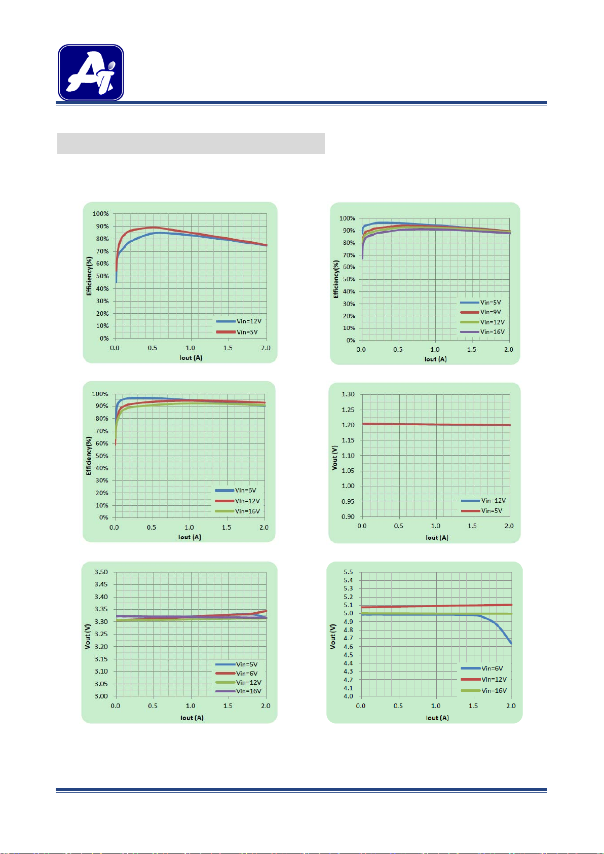
1. Efficiency vs. I
OUT
(V
OUT
= 1.2V)
2. Efficiency vs. I
OUT
(V
OUT
= 3.3V)
3. Efficiency vs. I
OUT
(V
OUT
= 5.0V)
4. V
OUT
vs. I
OUT
(V
OUT
= 1.2V)
5. V
OUT
vs. I
OUT
(V
OUT
= 3.3V)
6. V
OUT
vs. I
OUT
(V
OUT
= 5.0V)
TYPICAL PERFORMANCE CHARACTERISTICS
Tested under, L=4.7uH, T
= 25°C, unless otherwise specified
A
2A 16V 600kHz SYNCHRONOUS
REV1.0 - SEP 2016 RELEASED - - 4 -
Page 5

AiT Semiconductor Inc.
www.ait-ic.com
A7221B
DC-DC CONVERTER BUCK (STEP-DOWN)
7. Efficiency vs. Vin (I
OUT
= 1A)
8. V
OUT
vs. VIN (I
OUT
= 1A)
BLOCK DIAGRAM
2A 16V 600kHz SYNCHRONOUS
REV1.0 - SEP 2016 RELEASED - - 5 -
Page 6

AiT Semiconductor Inc.
www.ait-ic.com
A7221B
DC-DC CONVERTER BUCK (STEP-DOWN)
2A 16V 600kHz SYNCHRONOUS
DETAILED INFORMATION
Internal Regulator
The A7221B is a current mode step down DC/DC converter that provides excellent transient response with no
extra external compensation components. This device contains an internal, low resistance, high voltage
power MOSFET, and operates at a high 600k operating frequency to ensure a compact, high efficiency design
with excellent AC and DC performance.
Error Amplifier
The error amplifier compares the FB pin voltage with the internal FB reference (VFB) and outputs a current
proportional to the difference between the two. This output current is then used to charge or discharge the
internal compensation network to form the COMP voltage, which is used to control the power MOSFET
current. The optimized internal compensation network minimizes the external component counts and
simplifies the control loop design.
Internal Soft-Start
The soft-start is implemented to prevent the converter output voltage from overshooting during startup. When
the chip starts, the internal circuitry generates a soft-start voltage (SS) ramping up from 0V to 0.6V. When it is
lower than the internal reference (REF), SS overrides REF so the error amplifier uses SS as the reference.
When SS is higher than REF, REF regains control. The SS time is internally fixed to 1ms.
Over-Current-Protection and Hiccup
The A7221B has cycle-by-cycle over current limit when the inductor current peak value exceeds the set
current limit threshold. Meanwhile, output voltage starts to drop until FB is below the Under-Voltage (UV)
threshold, typically 30% below the reference. Once a UV is triggered, the A7221B enters hiccup mode to
periodically restart the part. This protection mode is especially useful when the output is dead-short to ground.
The average short circuit current is greatly reduced to alleviate the thermal issue and to protect the regulator.
The A7221B exits the hiccup mode once the over current condition is removed.
Startup and Shutdown
If both VIN and EN are higher than their appropriate thresholds, the chip starts. The reference block starts first,
generating stable reference voltage and currents, and then the internal regulator is enabled. The regulator
provides stable supply for the remaining circuitries. Three events can shut down the chip: EN low, V
thermal shutdown. In the shutdown procedure, the signaling path is first blocked to avoid any fault triggering.
The COMP voltage and the internal supply rail are then pulled down. The floating driver is not subject to this
shutdown command.
REV1.0 - SEP 2016 RELEASED - - 6 -
low and
IN
Page 7

AiT Semiconductor Inc.
www.ait-ic.com
A7221B
DC-DC CONVERTER BUCK (STEP-DOWN)
1/VV
R
FBOUT
1
−
OSC L
IN
OUTIN OUT
fx x ΔIV
)V(Vx V −
2
ΔI
L
+
−
2 S
ESR
IN
OUT
LS
OUT
Cx f x 8
1
R x
V
V
1x
x f
V
−
IN
OUT
2
2
s
OUT
V
V
1x
C x L x f x 8
V
2A 16V 600kHz SYNCHRONOUS
APPLICATIONS INFORMATION
Setting Output Voltages
The external resistor divider is used to set the output voltage (see Typical Application on page 1). The
feedback resistor R1 also sets the feedback loop bandwidth with the internal compensation capacitor. Choose
R1 to be around 100kΩ for optimal transient response. R2 is then given by:
R
=
2
Selecting the Inductor
A 4.7μH to 22μH inductor with a DC current rating of at least 25% percent higher than the maximum load
current is recommended for most applications. For highest efficiency, the inductor DC resistance should be
less than 15mΩ. For most designs, the inductance value can be derived from the following equation.
Where ΔI
L =
is the inductor ripple current. Choose inductor ripple current to be approximately 30% if the
L
maximum load current, 2A. The maximum inductor peak current is:
I
L(MAX)
= I
LOAD
+
Under light load conditions below 100mA, larger inductance is recommended for improved efficiency.
Selecting the Output Capacitor
The output capacitor (C2) is required to maintain the DC output voltage. Ceramic, tantalum, or low ESR
electrolytic capacitors are recommended. Low ESR capacitors are preferred to keep the output voltage ripple
low. The output voltage ripple can be estimated by:
ΔV
OUT
Where L is the inductor value and R
=
is the equivalent series resistance (ESR) value of the output capacitor.
ESR
In the case of ceramic capacitors, the impedance at the switching frequency is dominated by the capacitance.
The output voltage ripple is mainly caused by the capacitance. For simplification, the output voltage ripple can
be estimated by:
REV1.0 - SEP 2016 RELEASED - - 7 -
ΔV
=
OUT
Page 8

AiT Semiconductor Inc.
www.ait-ic.com
A7221B
DC-DC CONVERTER BUCK (STEP-DOWN)
ESR
IN
OUT
LS
OUT
R x
V
V
1x
x f
V
−
2A 16V 600kHz SYNCHRONOUS
In the case of tantalum or electrolytic capacitors, the ESR dominates the impedance at the switching
frequency. For simplification, the output ripple can be approximated to:
ΔV
OUT
=
The characteristics of the output capacitor also affect the stability of the regulation system. The A7221B can
be optimized for a wide range of capacitance and ESR values.
REV1.0 - SEP 2016 RELEASED - - 8 -
Page 9

AiT Semiconductor Inc.
www.ait-ic.com
A7221B
DC-DC CONVERTER BUCK (STEP-DOWN)
PACKAGE INFORMATION
Dimension in SOT-26 Package (Unit: mm)
2A 16V 600kHz SYNCHRONOUS
REV1.0 - SEP 2016 RELEASED - - 9 -
Page 10

AiT Semiconductor Inc.
www.ait-ic.com
A7221B
DC-DC CONVERTER BUCK (STEP-DOWN)
2A 16V 600kHz SYNCHRONOUS
IMPORTANT NOTICE
AiT Semiconductor Inc. (AiT) reserves the right to make changes to any its product, specifications, to
discontinue any integrated circuit product or service without notice, and advises its customers to obtain the
latest version of relevant information to verify, before placing orders, that the information being relied on is
current.
AiT Semiconductor Inc.'s integrated circuit products are not designed, intended, authorized, or warranted to
be suitable for use in life support applications, devices or systems or other critical applications. Use of AiT
products in such applications is understood to be fully at the risk of the customer. As used herein may involve
potential risks of death, personal injury, or servere property, or environmental damage. In order to minimize
risks associated with the customer's applications, the customer should provide adequate design and
operating safeguards.
AiT Semiconductor Inc. assumes to no liability to customer product design or application support. AiT
warrants the performance of its products of the specifications applicable at the time of sale.
REV1.0 - SEP 2016 RELEASED - - 10 -
Page 11

 Loading...