

Page 1
AiT Semiconductor Inc.
www.ait-ic.com
A7221A
DESCRIPTION
FEATURES
to minimize the
ORDERING INFORMATION
Package Type
Part Number
A7221AE6R
A7221AE6VR
APPLICATION
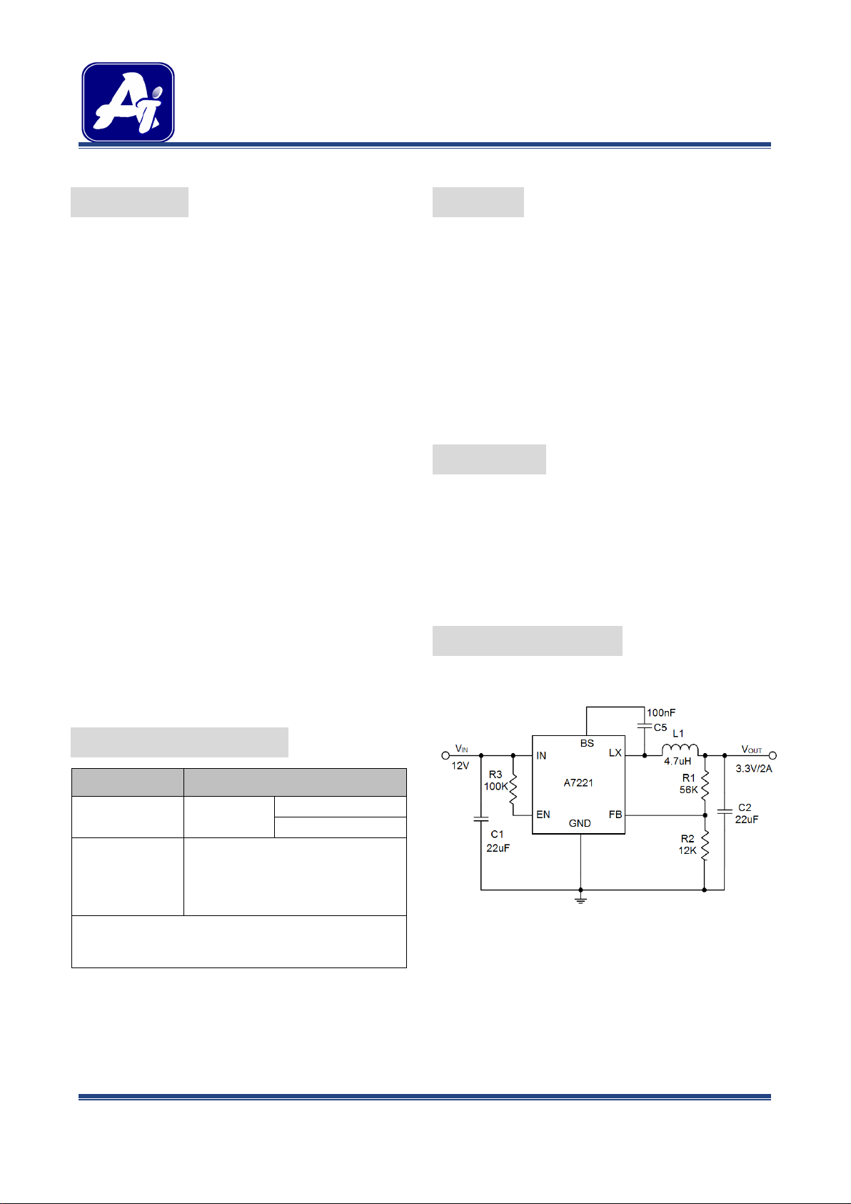
TYPICAL APPLICATION
DC-DC CONVERTER BUC K (STEP-DOWN)
2A, 16V SYNCHRONOUS
A7221A is simple, easy to use, 2A synchronous
step-down (Buck) convertor in SOT-26 package, with
high efficiency and fast transient response. A7221A
operates over a wide input voltage range from 4.5V to
16V and integrates main switch and synchronous
switch with very low R
DS(ON)
conduction loss. A7221A adopts the active constant
on time PWM architecture to achieve fast transient
responses for high step down applications and high
efficiency at light loads. In addition, it keeps in
constant frequency of 500kHz under heavy load
conditions to minimize the size of inductor and
capacitor. Fault conditions also include cycle-by-cycle
current limit, output under voltage protection, output
over current protection, output short-circuit protection
and thermal shutdown
Integrated 130mΩ and 120mΩ FETs
4.5~16V input voltage range
2A load current capability
Active constant on time PWM architecture with
500kHz switching frequency
Internal soft-start limits the inrush current
2% 0.6V reference
Available in SOT-26 Package
Set Top Box
Portable TV
Access Point Router
DSL Modem
LCD TV
The A7221A is available in SOT-26 package.
SOT-26 E6
V: Halogen free Package
Note
R: Tape & Reel
SPQ:3,000pcs/Reel
AiT provides all RoHS products
Suffix “ V “ means Halogen free Package
Figure 1. Typical Application Circuit
REV3.0 - DEC 2015 RELEASED, AUG 2016 UPDATED - - 1 -
Page 2
AiT Semiconductor Inc.
www.ait-ic.com
A7221A
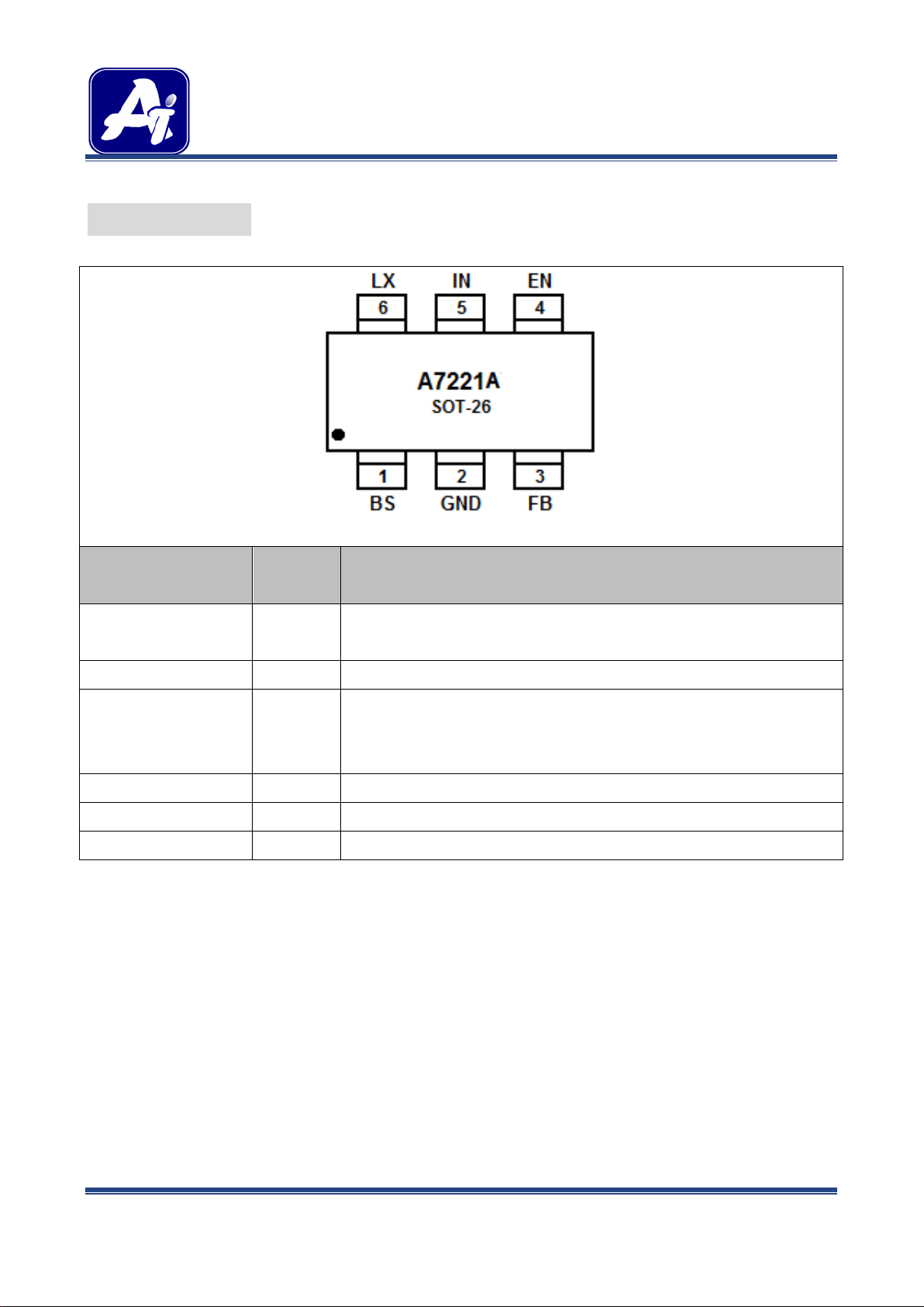
Pin #
Symbol
Function
PIN DESCRIPTION
DC-DC CONVERTER BUC K (STEP-DOWN)
2A, 16V SYNCHRONOUS
Top View
Boot-Strap Pin. Supply high side gate driver. Decouple this pin to LX
1 BS
pin with 0.1uF ceramic cap.
2 GND Ground pin.
Output Feedback Pin. Connect this pin to the center point of the output
3 FB
resistor divider (as shown in Figure 1) to program the output voltage:
V
=0.6x(1+R1/R2).
OUT
4 EN Enable control. Pull high to turn on. Do not float.
5 IN Input pin. Decouple this pin to GND pin with at least 1uF ceramic cap.
6 LX Inductor pin. Connect this pin to the switching node of inductor.
REV3.0 - DEC 2015 RELEASED, AUG 2016 UPDATED - - 2 -
Page 3
AiT Semiconductor Inc.
www.ait-ic.com
A7221A
Parameter
Symbol
Min.
Max.
Unit
DC-DC CONVERTER BUC K (STEP-DOWN)
2A, 16V SYNCHRONOUS
ABSOLUTE MAXIMUM RATINGS
VIN, Supply Voltage -0.3V ~ 18V
VSW, Switch Voltage -1V ~ VIN + 0.3V
VEN, Enable -1V ~ VIN + 0.3V
VBS, Bootstrap Voltage -0.3V ~ +4V
VFB, Feedback Voltage -0.3V~ +4V
Thermal Resistance
θJA 100℃/W
θJC 55℃/W
Junction Temperature +150℃
Lead Temperature (Soldering, 10s) +260℃
NOTE1
Storage Temperature -65℃~+150℃
Stress beyond above listed “Absolute Maximum Ratings” may lead permanent damage to the device. These are stress ratings only and
operations of the device at these or any other conditions beyond those indicated in the operational sections of the specifications are not
implied. Exposure to absolute maximum rating conditions for extended periods may affect device reliability.
NOTE1: Measured on approximately 1” square of 1oz copper.
RECOMMENDED OPERATING CONDITIONS
NOTE2
Input Voltage VIN 4.5 16 V
Operating Temperature -40 85 ℃
NOTE2: The device is not guaranteed to function outside of its operating conditions.
REV3.0 - DEC 2015 RELEASED, AUG 2016 UPDATED - - 3 -
Page 4
AiT Semiconductor Inc.
www.ait-ic.com
A7221A
Parameter
Conditions
Min.
Typ.
Max.
Unit
DC-DC CONVERTER BUC K (STEP-DOWN)
2A, 16V SYNCHRONOUS
ELECTRICAL CHARACTERISTICS
= 12V, V
V
IN
Shutdown Supply Current VEN=0V 10 20 μA
= 3.3V, L = 4.7uH, TA = 25°C, unless otherwise specified
OUT
Supply Current I
=0, VFB=V
OUT
×105% 350 μA
REF
Feedback Voltage 5V<VIN<16V 588 600 612 mV
FB Input Current -50 50 nA
High-Side Switch-On Resistance 130 mΩ
Low-Side Switch-On Resistance 120 mΩ
High-Side Switch Leakage VEN = 0V, VSW = 0V 0 10 μA
Upper Switch Current Limit 3.0 3.5 A
Lower Switch Current Limit 1.3 A
Oscillator Frequency 500 kHz
EN Rising Threshold 1.2 V
EN Falling Threshold 0.4 V
Input UVLO Threshold Rising VIN Rising 3.8 4.2 4.5 V
Input UVLO Threshold Hysteresis 15 mV
Min ON Time 50 ns
Soft-start Time tSS 0.2 ms
Max Duty Cycle 85 %
Thermal Shutdown 160 ℃
REV3.0 - DEC 2015 RELEASED, AUG 2016 UPDATED - - 4 -
Page 5
AiT Semiconductor Inc.
www.ait-ic.com
A7221A
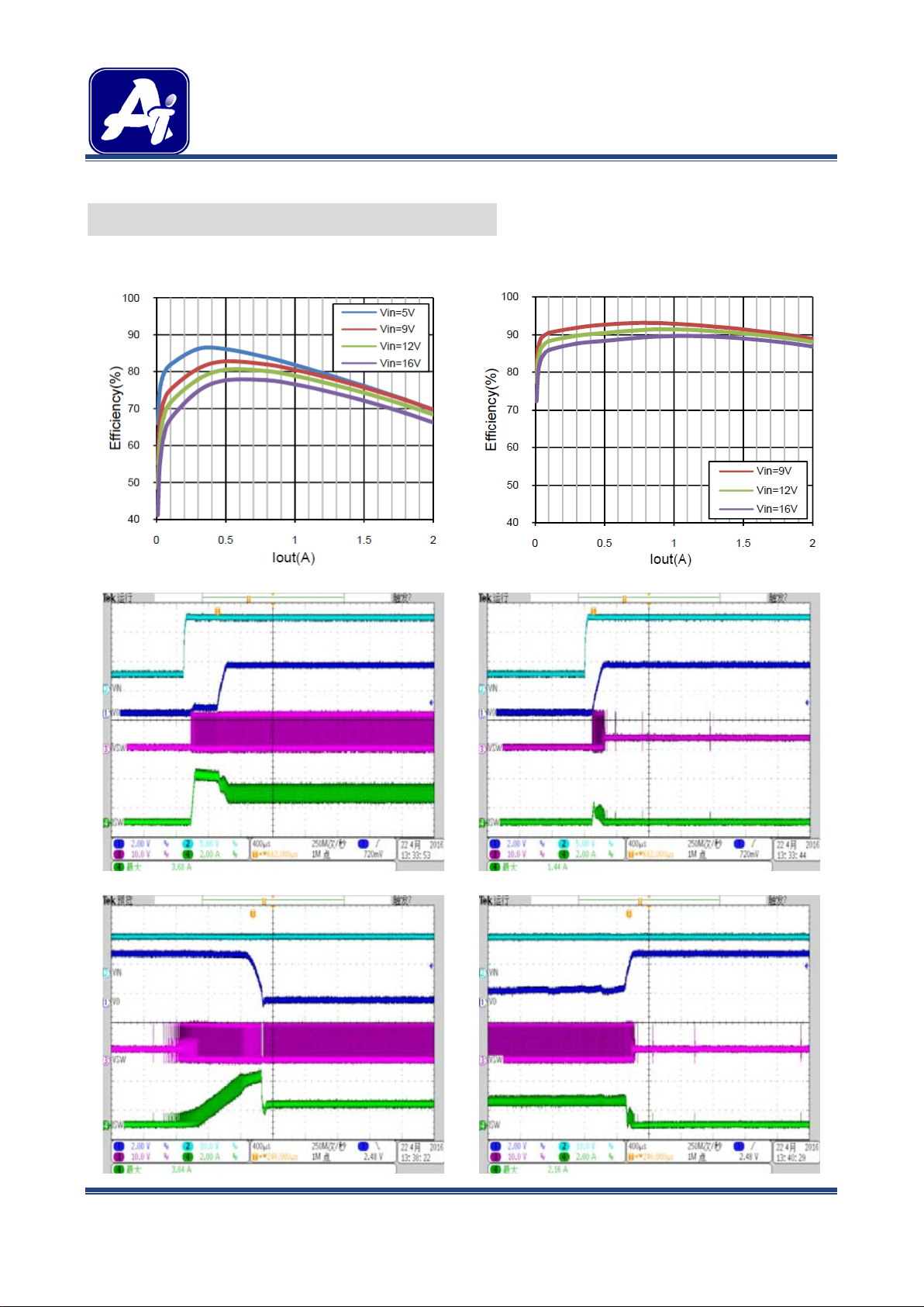
1. Efficiency vs. I
OUT
@V
OUT
=1.2V
2. Efficiency vs. I
OUT
@V
OUT
=5V
3. Soft-Start (V
IN
=12V, VO=3.3V, IO=2A)
4. Soft-Start (V
IN
=12V,VO=3.3V,IO=0A)
5. Short Circuit
6. Short Circuit Recovery
TYPICAL PERFORMANCE CHARACTERISTICS
DC-DC CONVERTER BUC K (STEP-DOWN)
2A, 16V SYNCHRONOUS
REV3.0 - DEC 2015 RELEASED, AUG 2016 UPDATED - - 5 -
Page 6

AiT Semiconductor Inc.
www.ait-ic.com
A7221A
7. Efficiency vs. I
OUT
@V
OUT
=3.3V
DC-DC CONVERTER BUC K (STEP-DOWN)
2A, 16V SYNCHRONOUS
REV3.0 - DEC 2015 RELEASED, AUG 2016 UPDATED - - 6 -
Page 7

AiT Semiconductor Inc.
www.ait-ic.com
A7221A
BLOCK DIAGRAM
DC-DC CONVERTER BUC K (STEP-DOWN)
2A, 16V SYNCHRONOUS
REV3.0 - DEC 2015 RELEASED, AUG 2016 UPDATED - - 7 -
Page 8

AiT Semiconductor Inc.
www.ait-ic.com
A7221A
R2R1R2+
R2
R1
L
S
OUT
x ΔIF
V
IN
OUT
V
V
DC-DC CONVERTER BUC K (STEP-DOWN)
2A, 16V SYNCHRONOUS
DETAILED INFORMATION
Operation
Functional Description
The A7221A is a synchronous rectified, current-mode, step-down regulator. It regulates input voltages from
4.5V to 16V down to an output voltage as low as 0.6V, and supplies up to 2A of load current.
The A7221A uses current-mode control to regulate the output voltage. The output voltage is measured at FB
through a resistive voltage divider and amplified through the internal transconductance error amplifier. The
converter uses internal N-Channel MOSFET switches to step-down the input voltage to the regulated output
voltage.
Application Information
Setting the Output Voltage
The output voltage is set using a resistive voltage divider from the output voltage to FB (see Typical
Application circuit on page 1). The voltage divider divides the output voltage down by the ratio:
V
Where V
is the feedback voltage and V
FB
= V
FB
is the output voltage.
OUT
OUT
x
Thus the output voltage is:
V
= 0.6 x (1+
OUT
)
Inductor
The inductor is required to supply constant current to the output load while being driven by the switched input
voltage. A larger value inductor will result in less ripple current that will result in lower output ripple voltage.
However, the larger value inductor will have a larger physical size, higher series resistance, and/or lower
saturation current. A good rule for determining the inductance to use is to allow the peak-to-peak ripple
current in the inductor to be approximately 30% of the maximum switch current limit. Also, make sure that the
peak inductor current is below the maximum switch current limit. The inductance value can be calculated by:
L =
x (1-
)
Where V
is the output voltage, VIN is the input voltage, fS is the switching frequency, and ΔIL is the
OUT
peak-to-peak inductor ripple current.
Choose an inductor that will not saturate under the maximum inductor peak current. The peak inductor current
can be calculated by:
REV3.0 - DEC 2015 RELEASED, AUG 2016 UPDATED - - 8 -
Page 9

AiT Semiconductor Inc.
www.ait-ic.com
A7221A
Lx F x 2
V
S
OUT
IN
OUT
V
V
Vendor
P/N
L(μH)
DCR(mΩ)
I
sat
(A)
IN
OUT
IN
OUT
V
V
)x
V
V
(1−
S
LOAD
F x C1
I
IN
OUT
V
V
IN
OUT
V
V
Lx F
V
S
OUT
IN
OUT
V
V
C2x F x 6.28
1
S
DC-DC CONVERTER BUC K (STEP-DOWN)
2A, 16V SYNCHRONOUS
here I
is the load current.
LOAD
ILP = I
LOAD
+
x (1-
)
The choice of which style inductor to use mainly depends on the price vs. size requirements and any EMI
requirements.
AiT-Components PIA6045-100MA 10 48 3.2
AiT-Components PIA5040-4R7N 4.7 30 3.5
Table 1. Recommended Inductors
Input Capacitor
The input current to the step-down converter is discontinuous, therefore a capacitor is required to supply the
AC current to the step-down converter while maintaining the DC input voltage. Use low ESR capacitors for the
best performance. Ceramic capacitors are preferred, but tantalum or low-ESR electrolytic capacitors may also
suffice. Choose X5R or X7R dielectrics when using ceramic capacitors. Since the input capacitor absorbs the
input switching current it requires an adequate ripple current rating. The RMS current in the input capacitor
can be estimated by:
I
The worst-case condition occurs at V
C1
= 2V
IN
= I
LOAD
, where I
OUT
CIN
= I
/2. For simplification, choose the input
LOAD
capacitor whose RMS current rating greater than half of the maximum load current. The input capacitor can
be electrolytic, tantalum or ceramic. When using electrolytic or tantalum capacitors, a small, high quality 0.1uF
ceramic capacitor should be placed as close to the IC as possible. When using ceramic capacitors, make sure
that they have enough capacitance to provide sufficient charge to prevent excessive voltage ripple at input.
The input voltage ripple for low ESR capacitors can be estimated by:
ΔV
IN =
x
x (1-
)
Where C1 s the value of the input capacitor.
Output Capacitor
The output capacitor is required to maintain the DC output voltage. Ceramic, tantalum, or low ESR electrolytic
capacitors are recommended. Low ESR capacitors are preferred to keep the output voltage ripple low. The
output voltage ripple can be estimated by:
ΔV
OUT =
x (1-
) x (R
ESR
+
)
REV3.0 - DEC 2015 RELEASED, AUG 2016 UPDATED - - 9 -
Page 10

AiT Semiconductor Inc.
www.ait-ic.com
A7221A
C2 x Lx F x 6.28
V
OUT
2
S
IN
OUT
V
V
Lx F
V
S
OUT
IN
OUT
V
V
V
OUT
R1(kΩ)
R2(kΩ)
L1(uH)
C1(uF)
C2(uF)
Where C2 is the output capacitance value and R
is the equivalent series resistance (ESR) value of the
ESR
DC-DC CONVERTER BUC K (STEP-DOWN)
2A, 16V SYNCHRONOUS
output capacitor. In the case of ceramic capacitors, the impedance at the switching frequency is dominated by
the capacitance. The output voltage ripple is mainly caused by the capacitance. For simplification, the output
voltage ripple can be estimated by:
ΔV
OUT
=
x (1-
)
In the case of tantalum or electrolytic capacitors, the ESR dominates the impedance at the switching
frequency. For simplification, the output ripple can be approximated to:
ΔV
OUT
=
x (1-
) x R
ESR
The characteristics of the output capacitor also affect the stability of the regulation system. The A7221A can
be optimized for a wide range of capacitance and ESR values. For A7221A normal operation, the input and
output can be an electrolytic capacitor in parallel.
5.0V 91 12 4.7 22 22
3.3V 53.6 12 4.7 22 22
2.5V 39 12 4.7 22 22
1.8V 24 12 4.7 22 22
1.5V 18 12 4.7 22 22
1.2V 12 12 4.7 22 22
1.0V 8.2 12 4.7 22 22
Table 2 Recommended Component Values for typical Output Voltage
Layout Guidance
When laying out the PCB board, the following suggestions should be taken to ensure proper operation of the
A7221A.
1. The power traces, including the GND trace, the SW trace and the V
trace should be kept short, direct
IN
and wide.
2. The FB pin should be connected directly to the feedback resistor. The resistive divider R1/R2 must be
connected between the (+) plate of C2 and ground.
3. Connect the (+) plate of C1 to the IN pin of A7221A as closely as possible. This capacitor provides the
AC current to internal power MOSFET.
4. Keep the switching node, SW, away from the sensitive V
5. Keep the (-) plates of C1 and C2 as close as possible.
REV3.0 - DEC 2015 RELEASED, AUG 2016 UPDATED - - 10 -
node.
FB
Page 11

AiT Semiconductor Inc.
www.ait-ic.com
A7221A
DC-DC CONVERTER BUC K (STEP-DOWN)
2A, 16V SYNCHRONOUS
REV3.0 - DEC 2015 RELEASED, AUG 2016 UPDATED - - 11 -
Page 12

AiT Semiconductor Inc.
www.ait-ic.com
A7221A
Symbol
Millimeters
Inches
Min
Max
Min
Max
PACKAGE INFORMATION
Dimension in SOT-26 Package (Unit: mm)
DC-DC CONVERTER BUC K (STEP-DOWN)
2A, 16V SYNCHRONOUS
A 1.050 1.250 0.041 0.049
A1 0.000 0.100 0.000 0.004
A2 1.050 1.150 0.041 0.045
b 0.300 0.500 0.012 0.020
c 0.100 0.200 0.004 0.008
D 2.820 3.020 0.111 0.119
E 1.500 1.700 0.059 0.067
E1 2.650 2.950 0.104 0.116
e 0.950(BSC) 0.037(BSC)
e1 1.800 2.000 0.071 0.079
L 0.300 0.600 0.012 0.024
θ 0° 8° 0° 8°
REV3.0 - DEC 2015 RELEASED, AUG 2016 UPDATED - - 12 -
Page 13

AiT Semiconductor Inc.
www.ait-ic.com
A7221A
DC-DC CONVERTER BUC K (STEP-DOWN)
2A, 16V SYNCHRONOUS
IMPORTANT NOTICE
AiT Semiconductor Inc. (AiT) reserves the right to make changes to any its product, specifications, to
discontinue any integrated circuit product or service without notice, and advises its customers to obtain the
latest version of relevant information to verify, before placing orders, that the information being relied on is
current.
AiT Semiconductor Inc.'s integrated circuit products are not designed, intended, authorized, or warranted to
be suitable for use in life support applications, devices or systems or other critical applications. Use of AiT
products in such applications is understood to be fully at the risk of the customer. As used herein may involve
potential risks of death, personal injury, or servere property, or environmental damage. In order to minimize
risks associated with the customer's applications, the customer should provide adequate design and
operating safeguards.
AiT Semiconductor Inc. assumes to no liability to customer product design or application support. AiT
warrants the performance of its products of the specifications applicable at the time of sale.
REV3.0 - DEC 2015 RELEASED, AUG 2016 UPDATED - - 13 -
Page 14

 Loading...