

Page 1
6B259
Data Sheet
26186.122
ADVANCE INFORMATION
(Subject to change without notice)
January 24, 2000
NO (INTERNAL)
CONNECTION
S (LSB)
GROUND
GROUND
Note that the A6B259KA (DIP) and the A6B259KLW
(SOIC) are electrically identical and share a common
terminal number assignment.
LOGIC
SUPPLY
0
OUT
OUT
OUT
OUT
LOGIC
POWER
1
NC
2
V
DD
3
4
0
5
1
6
2
7
3
8
S
1
9
10
LATCHES
DECODER LOGIC
LATCHES
ABSOLUTE MAXIMUM RATINGS
at T
= 25°C
Output Voltage, VO............................... 50 V
Output Drain Current,
Continuous, IO.......................... 150 mA*
Peak, IOM................................... 500 mA†
Single-Pulse Avalanche Energy,
EAS................................................. 30 mJ
Logic Supply Voltage, VDD.................. 7.0 V
Input Voltage Range,
VI................................... -0.3 V to +7.0 V
Package Power Dissipation,
PD........................................... See Graph
Operating Temperature Range,
TA................................. -40°C to +125°C
Storage Temperature Range,
TS................................. -55°C to +150°C
* Each output, all outputs on.
† Pulse duration ≤ 100 µs, duty cycle ≤ 2%.
Caution: These CMOS devices have input static
protection (Class 3) but are still susceptible to damage if
exposed to extremely high static electrical charges.
A
NC
EN
NO (INTERNAL)
CONNECTION
19
CLEAR
1820DATA
OUT
17
OUT
16
OUT
15
14
OUT
ENABLE
13
12
S (MSB)
2
POWER
11
GROUND
Dwg. PP-050-1
7
6
5
4
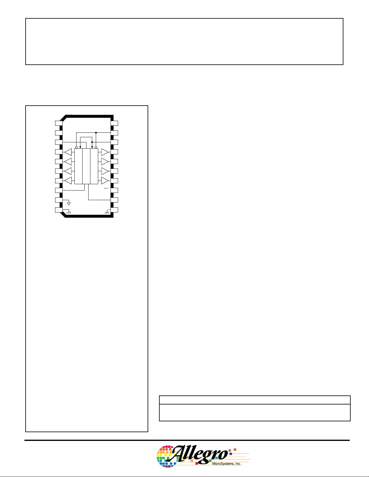
8-BIT ADDRESSABLE
DMOS POWER DRIVER
The A6B259KA and A6B259KLW combine a 3-to-8 line CMOS
decoder and accompanying data latches, control circuitry, and DMOS
outputs in a multi-functional power driver capable of storing single-line
data in the addressable latches or use as a decoder or demuliplexer.
Driver applications include relays, solenoids, and other mediumcurrent or high-voltage peripheral power loads.
The CMOS inputs and latches allow direct interfacing with microprocessor-based systems. Use with TTL may require appropriate pullup resistors to ensure an input logic high. Four modes of operation are
selectable with the CLEAR and ENABLE inputs.
The A6B259KA/KLW DMOS open-drain outputs are capable of
sinking up to 500 mA. Similar devices with reduced r
able as the A6259KA/KLW.
The A6B259KA is furnished in a 20-pin dual in-line plastic
package. The A6B259KLW is furnished in a 20-lead wide-body,
small-outline plastic package (SOIC) with gull-wing leads for surfacemount applications. Copper lead frames, reduced supply current
requirements, and low on-state resistance allow either device to sink
150 mA from all outputs continuously, to ambient temperatures greater
than 85°C.
FEATURES
■ 50 V Minimum Output Clamp Voltage
■ 150 mA Output Current (all outputs simultaneously)
■ 5 Ω Typical
■ Low Power Consumption
■ Replacements for TPIC6B259N and TPIC6B259DW
Always order by complete part number:
Part Number Package R
A6B259KA 20-pin DIP 55°C/W 25°C/W
A6B259KLW 20-lead SOIC 70°C/W 17°C/W
r
DS(on)
θJA
DS(on)
are avail-
R
θJC
Page 2
6B259
g
8-BIT ADDRESSABLE
DMOS POWER DRIVER
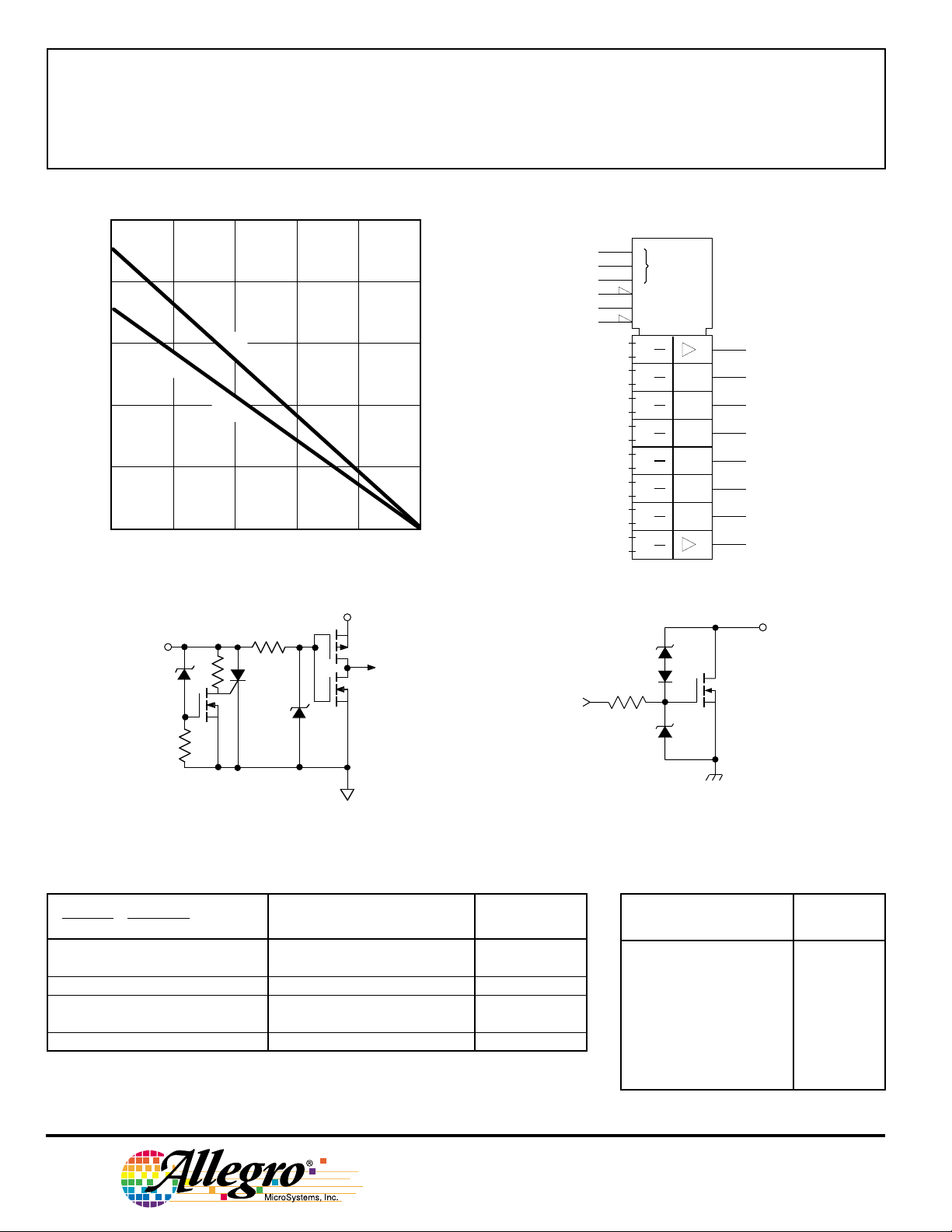
2.5
2.0
SUFFIX 'A', R = 55
1.5
1.0
SUFFIX 'LW
θ
J
A
', R = 70
θ
J
A
°C/W
°C/W
0.5
0
25
ALLOWABLE PACKAGE POWER DISSIPATION IN WATTS
50 75 100 125 150
AMBIENT TEMPERATURE IN °C
Dwg. GS-004A
V
DD
IN
LOGIC SYMBOL
3
8
12
13
18
19
0
2
G8
Z9
Z10
9,0D
10,0R
9,1D
10,1R
9,2D
10,2R
9,3D
10,3R
9,4D
10,4R
9,5D
10,5R
9,6D
10,6R
9,7D
10,7R
8M 0/7
Dw
4
5
6
7
14
15
16
17
. FP-046
OUT
Dwg. EP-010-15
FUNCTION TABLE
Inputs
CLEAR ENABLE DATA OUTPUT OUTPUTs Function
HLH L R
HLL H R
H H X R R Memory
LLH L H
LLL H H
L H X H H Clear
L = Low Logic Level H = High Logic Level X = Irrelevant R = Previous State
Addressed Other
115 Northeast Cutoff, Box 15036
Worcester, Massachusetts 01615-0036 (508) 853-5000
W
Copyright © 2000, Allegro MicroSystems, Inc.
DMOS POWER DRIVER OUTPUTLOGIC INPUTS
Addressable
Latch
8-Line
Demultiplexer
Dwg. EP-063
LATCH SELECTION TABLE
Select Inputs
S2 (MSB)S1S0 (LSB) OUTPUT
LLL 0
LLH 1
LHL 2
LHH 3
HLL 4
HLH 5
HHL 6
HHH 7
Addressed
Page 3
8-BIT ADDRESSABLE
DMOS POWER DRIVER
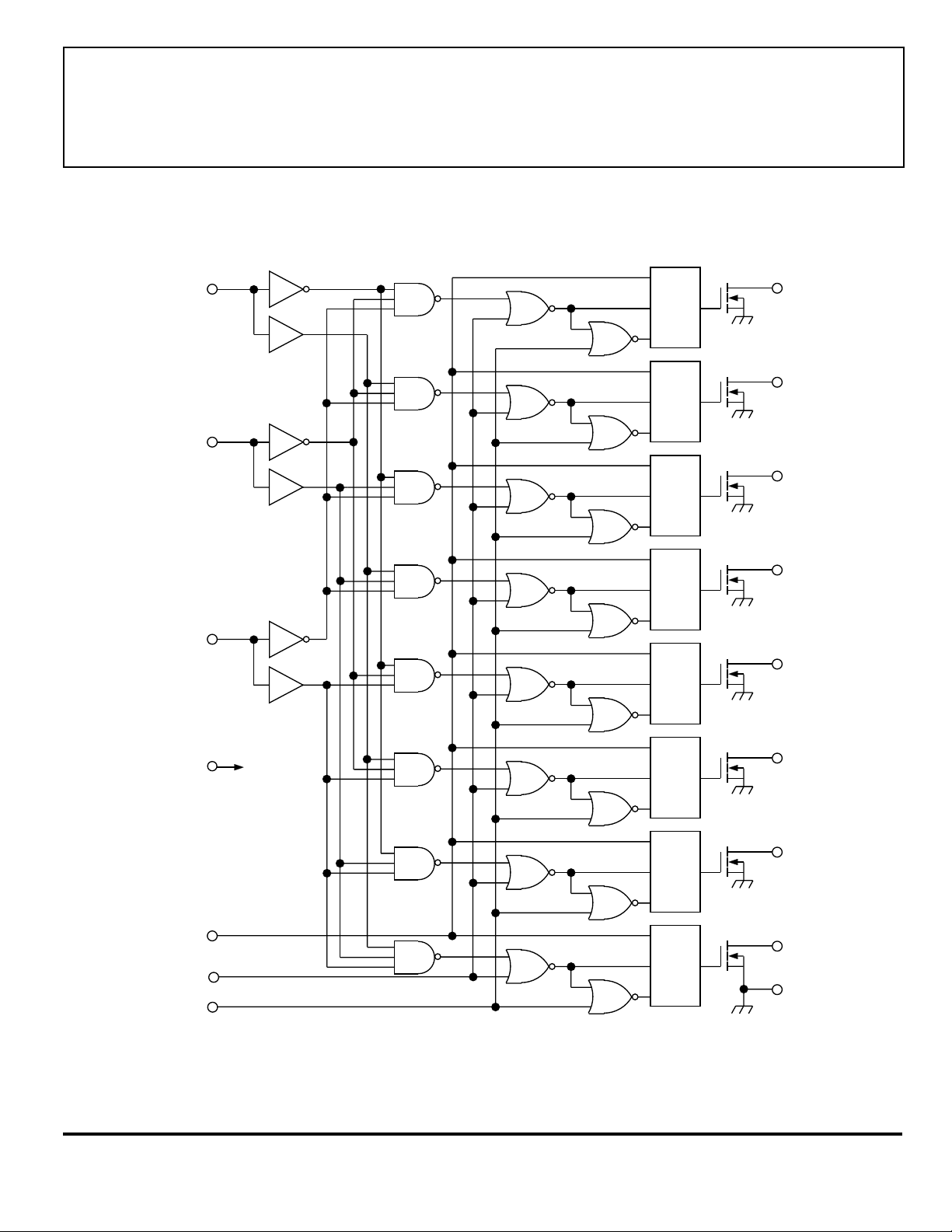
FUNCTIONAL BLOCK DIAGRAM
6B259
(LSB)
(MSB)
S
0
S
1
S
2
D
C1
CLR
D
C1
CLR
D
C1
CLR
D
C1
CLR
D
C1
CLR
OUT
OUT
OUT
OUT
OUT
0
1
2
3
4
LOGIC
SUPPLY
DATA
ENABLE
(ACTIVE LOW)
CLEAR
(ACTIVE LOW)
www.allegromicro.com
D
V
DD
C1
CLR
D
C1
CLR
D
C1
CLR
Grounds (terminals 9, 10, and 11) must be connected externally to a single point.
OUT
5
OUT
6
OUT
7
GROUND
Dwg. FP-047
Page 4
6B259
8-BIT ADDRESSABLE
DMOS POWER DRIVER
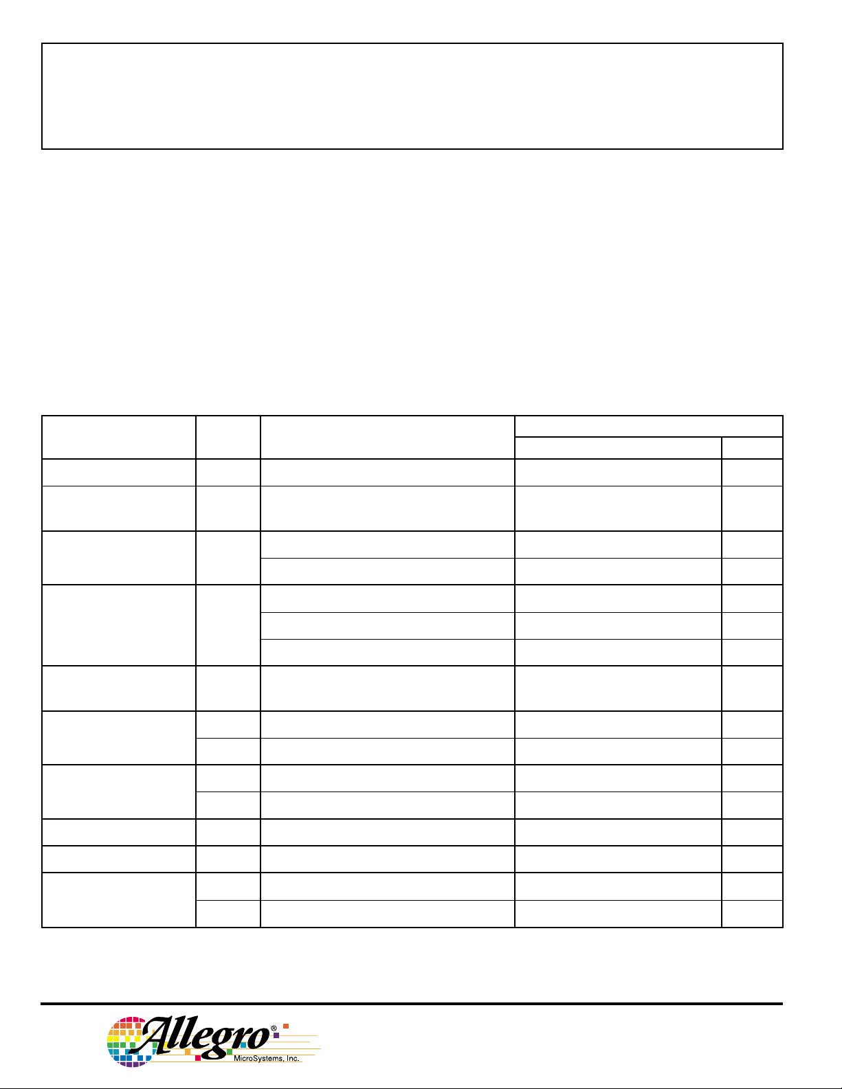
RECOMMENDED OPERATING CONDITIONS
over operating temperature range
Logic Supply Voltage Range, VDD............... 4.5 V to 5.5 V
High-Level Input Voltage, V
Low-level input voltage, V
............................ ≥ 0.85V
IH
................................. ≤0.15V
IL
DD
DD
ELECTRICAL CHARACTERISTICS at T
= +25°C, V
A
= 5 V, tir = t
DD
≤ 10 ns (unless otherwise
if
specified).
Limits
Characteristic Symbol Test Conditions Min. Typ. Max. Units
Logic Supply Voltage V
Output Breakdown V
(BR)DSXIO
Voltage
Off-State Output I
Current
Static Drain-Source r
On-State Resistance
Nominal Output I
Current
Logic Input Current I
Prop. Delay Time t
DD
DSX
DS(on)
ON
IH
I
IL
PLH
Operating 4.5 5.0 5.5 V
= 1 mA 50 — — V
VO = 40 V, V
VO = 40 V, VDD = 5.5 V, T
IO = 100 mA, V
IO = 100 mA, VDD = 4.5 V, T
IO = 350 mA, V
V
= 0.5 V, T
DS(on)
VI = V
DD
VI = 0, V
= 5.5 V — 0.1 5.0 µA
DD
= 125°C — 0.15 8.0 µA
A
= 4.5 V — 4.2 5.7 Ω
DD
= 125°C— 6.8 9.5 Ω
A
= 4.5 V (see note) — 5.5 8.0 Ω
DD
= 85°C—90—mA
A
= 5.5 V — — 1.0 µA
= 5.5 V — — -1.0 µA
DD
IO = 100 mA, CL = 30 pF — 150 — ns
Output Rise Time t
Output Fall Time t
Supply Current I
DD(OFF)
I
DD(ON)
t
PHL
r
f
IO = 100 mA, CL = 30 pF — 90 — ns
IO = 100 mA, CL = 30 pF — 200 — ns
IO = 100 mA, CL = 30 pF — 200 — ns
V
= 5.5 V, Outputs off — 20 100 µA
DD
V
= 5.5 V, Outputs on — 150 300 µA
DD
Typical Data is at VDD = 5 V and is for design information only.
NOTE — Pulse test, duration ≤100 µs, duty cycle ≤2%.
115 Northeast Cutoff, Box 15036
Worcester, Massachusetts 01615-0036 (508) 853-5000
Page 5

8-BIT ADDRESSABLE
DMOS POWER DRIVER
FUNCTIONAL DESCRIPTION and INPUT REQUIREMENTS
6B259
ENABLE
DATA
ADDRESSED
OUTPUT
50%
t
PLH
10%
t
r
t
PHL
90%
t
f
Dwg. WP-036
OUTPUT SWITCHING TIME
su(D)
50%
t
h(D)
t
w(D)
Dwg. WP-037
ENABLE
DATA
t
50%
DATA INPUT REQUIREMENTS
Data Active Time Before Enable
(Data Set-Up Time), t
Data Active Time After Enable
(Data Hold Time), t
Data Pulse Width, t
w(D)
Input Logic High, VIH................................................ ≥ 0.85V
Input Logic Low, VIL................................................. ≤ 0.15V
.............................................. 20 ns
su(D)
................................................... 20 ns
h(D)
....................................................... 40 ns
Four modes of operation are selectable by controlling
the CLEAR and ENABLE inputs as shown above.
In the addressable-latch mode, data at the DATA input
is written into the addressed transparent latch. The
addressed output inverts the data input with all other
outputs remaining in their previous states.
In the memory mode, all outputs remain in their
previous states and are unaffected by the DATA or
address (S
) inputs. To prevent entering erroneus data in
n
the latches, ENABLE should be held HIGH while the
address lines are changing.
In the demultiplexing/decoding mode, the addressed
output inverts the data input and all other outputs are OFF.
In the clear mode, all outputs are OFF and are unaffected by the DATA or address (S
) inputs.
N
Given the appropriate inputs, when DATA is LOW
for a given address, the output is OFF; when DATA is
HIGH, the output is ON and can sink current.
CC
CC
www.allegromicro.com
Page 6

6B259
8-BIT ADDRESSABLE
DMOS POWER DRIVER
TEST CIRCUITS
INPUT
I
O
V
O
t
av
IAS = 500 mA
V
(BR)DSX
V
O(ON)
EAS = IAS x V
(BR)DSX
DUT
x tAV/2
+15 V
10.5 Ω
200 mH
OUT
Dwg. EP-066
Single-Pulse Avalanche Energy Test Circuit
and Waveforms
115 Northeast Cutoff, Box 15036
Worcester, Massachusetts 01615-0036 (508) 853-5000
Page 7

DMOS POWER DRIVER
TYPICAL CHARACTERISTICS
6B259
8-BIT ADDRESSABLE
www.allegromicro.com
Page 8

6B259
8-BIT ADDRESSABLE
DMOS POWER DRIVER
TYPICAL CHARACTERISTICS
115 Northeast Cutoff, Box 15036
Worcester, Massachusetts 01615-0036 (508) 853-5000
Page 9

8-BIT ADDRESSABLE
DMOS POWER DRIVER
TERMINAL DESCRIPTIONS
Terminal No. Terminal Name Function
1 NC No (internal) connection.
2 LOGIC SUPPLY (VDD) The logic supply voltage (typically 5 V).
3S0Binary-coded output-select input, least-significant bit.
6B259
4 OUT
5 OUT
6 OUT
7 OUT
0
1
2
3
Current-sinking, open-drain DMOS output, address 000.
Current-sinking, open-drain DMOS output, address 001.
Current-sinking, open-drain DMOS output, address 010.
Current-sinking, open-drain DMOS output, address 011.
8S1Binary-coded output-select input.
9 LOGIC GROUND Reference terminal for logic voltage measurements.
10 POWER GROUND Reference terminal for output voltage measurements (OUT
11 POWER GROUND Reference terminal for output voltage measurements (OUT
12 S
2
Binary-coded output-select input, most-significant bit.
0-3
4-7
).
).
13 ENABLE Mode control input; see Function Table.
14 OUT
15 OUT
16 OUT
17 OUT
4
5
6
7
Current-sinking, open-drain DMOS output, address 100.
Current-sinking, open-drain DMOS output, address 101.
Current-sinking, open-drain DMOS output, address 110.
Current-sinking, open-drain DMOS output, address 111.
18 DATA CMOS data input to the addressed output latch. When enabled, the
addressed output inverts the data input (DATA = HIGH, OUTPUT = LOW).
19 CLEAR Mode control input; see Function Table.
20 NC No (internal) connection.
NOTE — Grounds (terminals 9, 10, and 11) must be connected externally to a single point.
www.allegromicro.com
Page 10

6B259
8-BIT ADDRESSABLE
DMOS POWER DRIVER
20
0.280
0.240
A6B259KA
Dimensions in Inches
(controlling dimensions)
11
0.014
0.008
0.300
BSC
0.430
MAX
0.210
MAX
7.11
6.10
0.015
MIN
1
0.070
0.045
0.022
0.014
1.060
0.980
0.100
BSC
10
0.005
MIN
0.150
0.115
Dwg. MA-001-20 in
Dimensions in Millimeters
(for reference only)
0.355
20
1
1.77
1.15
26.92
24.89
2.54
BSC
11
10
0.13
MIN
0.204
7.62
BSC
10.92
MAX
5.33
MAX
0.39
MIN
0.558
0.356
3.81
2.93
NOTES: 1. Exact body and lead configuration at vendor’s option within limits shown.
2. Lead spacing tolerance is non-cumulative.
3. Lead thickness is measured at seating plane or below.
115 Northeast Cutoff, Box 15036
Worcester, Massachusetts 01615-0036 (508) 853-5000
Dwg. MA-001-20 mm
Page 11

A6B259KLW
Dimensions in Inches
(for reference only)
6B259
8-BIT ADDRESSABLE
DMOS POWER DRIVER
20 11
0.2992
0.2914
0.020
1 2
0.013
0.0926
0.1043
0.0040
3
MIN.
20
0.050
0.5118
0.4961
BSC
Dimensions in Millimeters
(controlling dimensions)
11
0.419
0.394
0° TO 8°
0.0125
0.0091
0.050
0.016
Dwg. MA-008-20 in
0.32
0.23
7.60
7.40
0.51
0.33
2.65
2.35
1
0.10
2
MIN.
3
13.00
12.60
1.27
BSC
10.65
10.00
NOTES: 1. Exact body and lead configuration at vendor’s option within limits shown.
2. Lead spacing tolerance is non-cumulative.
www.allegromicro.com
0° TO 8°
Dwg. MA-008-20 mm
1.27
0.40
Page 12

6B259
8-BIT ADDRESSABLE
DMOS POWER DRIVER
The products described here are manufactured under one or more
U.S. patents or U.S. patents pending.
Allegro MicroSystems, Inc. reserves the right to make, from time to
time, such departures from the detail specifications as may be
required to permit improvements in the performance, reliability, or
manufacturability of its products. Before placing an order, the user is
cautioned to verify that the information being relied upon is current.
Allegro products are not authorized for use as critical components
in life-support devices or systems without express written approval.
The information included herein is believed to be accurate and
reliable. However, Allegro MicroSystems, Inc. assumes no responsibility for its use; nor for any infringement of patents or other rights of
third parties which may result from its use.
115 Northeast Cutoff, Box 15036
Worcester, Massachusetts 01615-0036 (508) 853-5000
 Loading...