

Page 1
A6275ELW
Data Sheet
26185.200
8-BIT SERIAL-INPUT, CONSTANTCURRENT LATCHED LED DRIVER
Always order by complete part number, e.g., A6275EA .
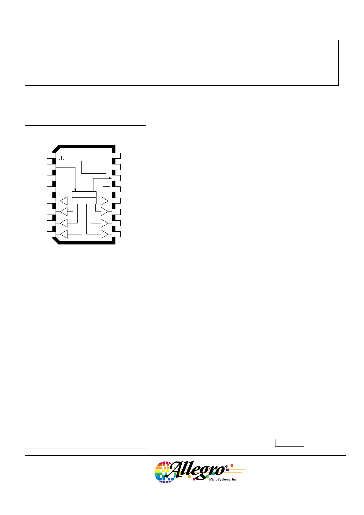
The A6275EA and A6275ELW are specifically designed for LEDdisplay applications. Each BiCMOS device includes an 8-bit CMOS
shift register, accompanying data latches, and eight npn constantcurrent sink drivers. Except for package style and allowable package
power dissipation, the two devices are identical.
The CMOS shift register and latches allow direct interfacing with
microprocessor-based systems. With a 5 V logic supply, typical serial
data-input rates are up to 20 MHz. The LED drive current is determined by the user’s selection of a single resistor. A CMOS serial data
output permits cascade connections in applications requiring additional
drive lines. For inter-digit blanking, all output drivers can be disabled
with an ENABLE input high. Similar 16-bit devices are available as
the A6276EA and A6276ELW.
Two package styles are provided for through-hole DIP (suffix A) or
surface-mount SOIC (suffix LW). Under normal applications, copper
lead frames and low logic-power dissipation allow these devices to
sink maximum rated current through all outputs continuously over the
operating temperature range (90 mA, 0.9 V drop, +85°C). Both
devices are also available for operation over the standard temperature
range of -20°C to +85°C. To order, change the suffix letter ‘E’ to ‘S’.
ABSOLUTE MAXIMUM RATINGS
Supply Voltage, VDD...................... 7.0 V
Output Voltage Range,
V
O
............................ -0.5 V to +17 V
Output Current, I
O
........................ 90 mA
Ground Current, I
GND
................. 750 mA
Input Voltage Range,
V
I
.................... -0.4 V to VDD + 0.4 V
Package Power Dissipation,
P
D
..................................... See Graph
Operating Temperature Range,
TA............................. -40°C to +85°C
Storage Temperature Range,
T
S
........................... -55°C to +150°C
Caution: These CMOS devices have input
static protection (Class 2) but are still susceptible to damage if exposed to extremely high
static electrical charges.
GROUND
REGISTER
LATCHES
1
2
3
89
10
11
12
13
15
4
5
6
7
14
16
SERIAL
DATA OUT
LOGIC
SUPPLY
SERIAL
DATA IN
OUTPUT
ENABLE
LATCH
ENABLE
CLOCK CK
V
DD
OE
OUT
1
OUT
2
Dwg. PP-029-10
OUT
0
OUT
4
OUT
6
OUT
5
OUT
3
OUT
7
R
EXT
I
REGULATOR
L
O
Note that the A6275EA (DIP) and the A6275ELW
(SOIC) are electrically identical and share a
common terminal number assignment.
6275
FEATURES
■ To 90 mA Constant-Current Outputs
■ Under-Voltage Lockout
■ Low-Power CMOS Logic and Latches
■ High Data Input Rate
■ Pin-Compatible with TB62705CP
Page 2
115 Northeast Cutoff, Box 15036
Worcester, Massachusetts 01615-0036 (508) 853-5000
6275
8-BIT SERIAL-INPUT,
CONSTANT-CURRENT
LATCHED LED DRIVER
2
Copyright © 2000, Allegro MicroSystems, Inc.
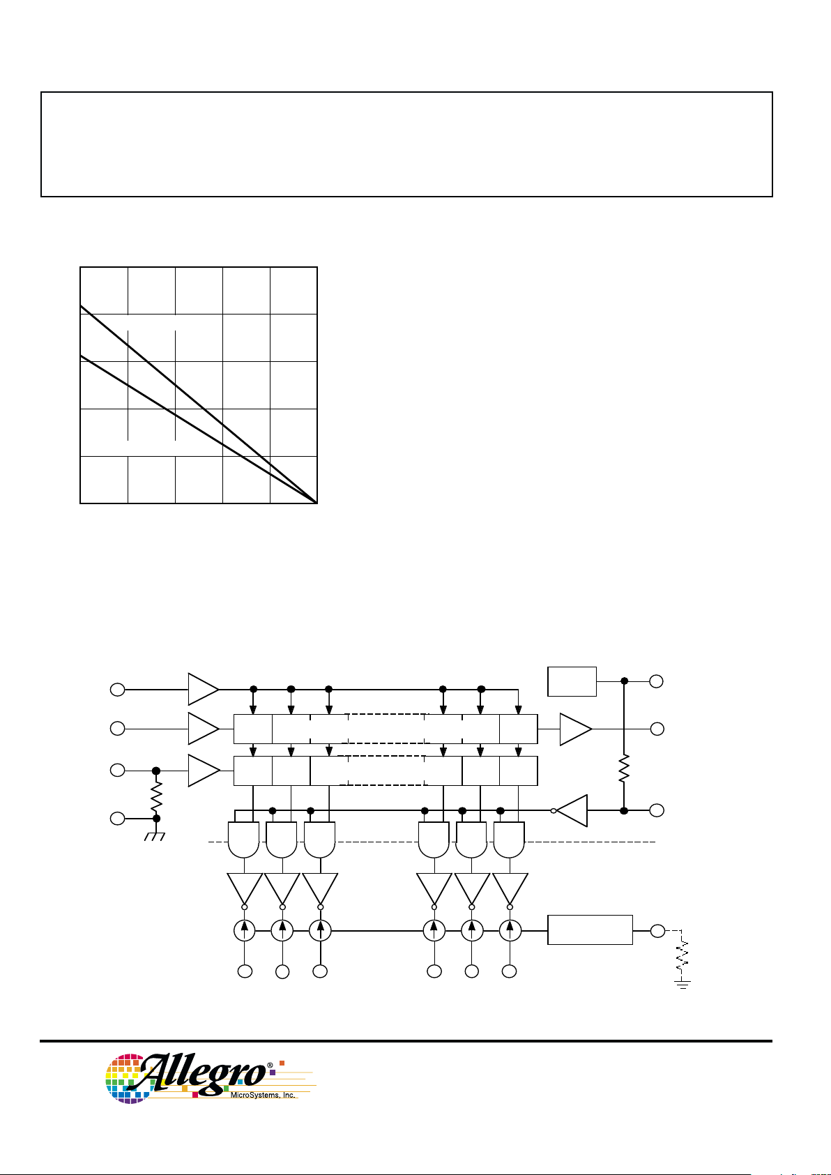
50 75 100 125 150
2.5
0.5
0
AMBIENT TEMPERATURE IN °C
2.0
1.5
1.0
25
Dwg. GP-018B
SUFFIX 'A', R = 60°C/W
θJA
SUFFIX 'LW', R = 80°C/W
θJA
ALLOWABLE PACKAGE POWER DISSIPATION IN WATTS
FUNCTIONAL BLOCK DIAGRAM
MOS
BIPOLAR
GROUND
LATCH
ENABLE
OUTPUT ENABLE
(ACTIVE LOW)
SERIAL
DATA OUT
CLOCK
SERIAL
DATA IN
SERIAL-PARALLEL SHIFT REGISTER
LATCHES
V
DD
LOGIC
SUPPLY
R
EXT
OUT0OUT
1
Dwg. FP-013-3
OUT
2
OUT
N
I
REGULATOR
O
UVLO
Page 3
6275
8-BIT SERIAL-INPUT,
CONSTANT-CURRENT
LATCHED LED DRIVER
www.allegromicro.com
3
CLOCK and SERIAL DATA IN SERIAL DATA OUT
LATCH ENABLEOUTPUT ENABLE (active low)
Dwg. EP-010-6
IN
V
DD
Dwg. EP-010-7
IN
V
DD
Dwg. EP-010-5
IN
V
DD
Dwg. EP-063-1
V
DD
OUT
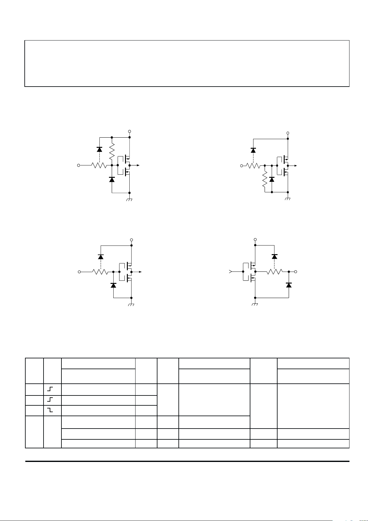
TRUTH TABLE
Serial Shift Register Contents Serial Latch Latch Contents Output Output Contents
Data Clock Data Enable Enable
Input Input I
1I2I3
... I
N-1IN
Output Input I1I2I3... I
N-1IN
Input I1I2I3... I
N-1
I
N
HHR
1R2
... R
N-2RN-1
R
N-1
LLR
1R2
... R
N-2RN-1
R
N-1
XR
1R2R3
... R
N-1RN
R
N
XXX...X X X L R1R2R3... R
N-1 RN
P1P2P3... P
N-1PN
P
N
HP1P2P3... P
N-1 PN
LP1P2P3... P
N-1 PN
XXX...X X H H H H ... H H
L = Low Logic (Voltage) Level H = High Logic (Voltage) Level X = Irrelevant P = Present State R = Previous State
Page 4
115 Northeast Cutoff, Box 15036
Worcester, Massachusetts 01615-0036 (508) 853-5000
6275
8-BIT SERIAL-INPUT,
CONSTANT-CURRENT
LATCHED LED DRIVER
4
ELECTRICAL CHARACTERISTICS at TA = +25°C, VDD = 5 V (unless otherwise noted).
Limits
Characteristic Symbol Test Conditions Min. Typ. Max. Unit
Supply Voltage Range V
DD
Operating 4.5 5.0 5.5 V
Under-Voltage Lockout V
DD(UV)
VDD = 0 → 5 V 3.4 – 4.0 V
Output Current I
O
VCE = 0.7 V, R
EXT
= 250 Ω 64.2 75.5 86.8 mA
(any single output)
VCE = 0.7 V, R
EXT
= 470 Ω 34.1 40.0 45.9 mA
Output Current Matching ∆I
O
0.4 V ≤ V
CE(A)
= V
CE(B)
≤ 0.7 V:
(difference between any R
EXT
= 250 Ω – ±1.5 ±6.0 %
two outputs at same VCE)
R
EXT
= 470 Ω – ±1.5 ±6.0 %
Output Leakage Current I
CEX
VOH = 15 V – 1.0 5.0 µA
Logic Input Voltage V
IH
0.7V
DD
–VDDV
V
IL
GND – 0.3V
DD
V
SERIAL DATA OUT V
OL
IOL = 500 µA––0.4V
Voltage
V
OH
IOH = -500 µ4A4.6––V
Input Resistance R
I
ENABLE Input, Pull Up 150 300 600 kΩ
LATCH Input, Pull Down 100 200 400 kΩ
Supply Current I
DD(OFF)
R
EXT
= open, VOE = 5 V – 0.8 1.4 mA
R
EXT
= 470 Ω, VOE = 5 V 3.5 6.0 8.0 mA
R
EXT
= 250 Ω, VOE = 5 V 6.5 11 15 mA
I
DD(ON)
R
EXT
= 470 Ω, VOE = 0 V 5.0 10 14 mA
R
EXT
= 250 Ω, VOE = 0 V 8.0 16 24 mA
Typical Data is at VDD = 5 V and is for design information only.
Page 5

6275
8-BIT SERIAL-INPUT,
CONSTANT-CURRENT
LATCHED LED DRIVER
www.allegromicro.com
5
RECOMMENDED OPERATING CONDITIONS
Characteristic Symbol Conditions Min. Typ. Max. Unit
Supply Voltage V
DD
4.5 5.0 5.5 V
Output Voltage V
O
-1.04.0 V
Output Current I
O
Continuous, any one output - - 90 mA
I
OH
SERIAL DATA OUT - - -1.0 mA
I
OL
SERIAL DATA OUT - - 1.0 mA
Logic Input Voltage V
IH
0.7V
DD
-VDD + 0.3 V
V
IL
-0.3 - 0.3V
DD
V
Clock Frequency f
CK
Cascade operation - - 10 MHz
SWITCHING CHARACTERISTICS at TA = 25°C, VDD = VIH = 5 V, VCE = 0.4 V, VIL = 0 V,
R
EXT
= 470 Ω, IO = 40 mA, VL = 3 V, RL = 65 Ω, CL = 10.5 pF.
Limits
Characteristic Symbol Test Conditions Min. Typ. Max. Unit
Propagation Delay Time t
pHL
CLOCK-OUT
n
– 350 1000 ns
LATCH-OUT
n
– 350 1000 ns
ENABLE-OUT
n
– 350 1000 ns
CLOCK-SERIAL DATA OUT – 80 110 ns
Propagation Delay Time t
pLH
CLOCK-OUT
n
– 300 1000 ns
LATCH-OUT
n
– 300 1000 ns
ENABLE-OUT
n
– 300 1000 ns
CLOCK-SERIAL DATA OUT – 80 110 ns
Output Fall Time t
f
90% to 10% voltage 150 350 1000 ns
Output Rise Time t
r
10% to 90% voltage 150 300 600 ns
Page 6

115 Northeast Cutoff, Box 15036
Worcester, Massachusetts 01615-0036 (508) 853-5000
6275
8-BIT SERIAL-INPUT,
CONSTANT-CURRENT
LATCHED LED DRIVER
6
TIMING REQUIREMENTS and SPECIFICATIONS
(Logic Levels are VDD and Ground)
A. Data Active Time Before Clock Pulse
(Data Set-Up Time), t
su(D)
.......................................... 60 ns
B. Data Active Time After Clock Pulse
(Data Hold Time), t
h(D)
.............................................. 20 ns
C. Clock Pulse Width, t
w(CK)
............................................... 50 ns
D. Time Between Clock Activation
and Latch Enable, t
su(L)
............................................ 100 ns
E. Latch Enable Pulse Width, t
w(L)
................................... 100 ns
F. Output Enable Pulse Width, t
w(OE)
................................ 4.5 µs
NOTE – Timing is representative of a 10 MHz clock.
Significantly higher speeds are attainable.
— Max. Clock Transition Time, tr or tf.............................. 10 µs
Information present at any register is transferred to the
respective latch when the LATCH ENABLE is high (serial-toparallel conversion). The latches will continue to accept new
data as long as the LATCH ENABLE is held high. Applications where the latches are bypassed (LATCH ENABLE tied
high) will require that the OUTPUT ENABLE input be high
during serial data entry.
When the OUTPUT ENABLE input is high, the output
source drivers are disabled (OFF). The information stored in the
latches is not affected by the OUTPUT ENABLE input. With
the OUTPUT ENABLE input low, the outputs are controlled by
the state of their respective latches.
CLOCK
SERIAL
DATA IN
LATCH
ENABLE
OUTPUT
ENABLE
OUT
N
Dwg. WP-029-1
50%
SERIAL
DATA OUT
DATA
DATA
50%
50%
50%
C
A B
D E
LOW = ALL OUTPUTS ENABLED
p
t
DATA
50%
p
t
LOW = OUTPUT ON
HIGH = OUTPUT OFF
OUTPUT
ENABLE
OUT
N
Dwg. WP-030-1
DATA
10%
50%
dis(BQ)
t
F
en(BQ)
t
HIGH = ALL OUTPUTS DISABLED (BLANKED)
ftr
t
90%
Page 7

6275
8-BIT SERIAL-INPUT,
CONSTANT-CURRENT
LATCHED LED DRIVER
www.allegromicro.com
7
ALLOWABLE OUTPUT CURRENT AS A FUNCTION OF DUTY CYCLE
A6275EA A6275ELW
0 20
DUTY CYCLE IN PER CENT
100
0
Dwg. GP-062-5
ALLOWABLE OUTPUT CURRENT IN mA/BIT
6040
20
40
60
10080
VCE = 2 V
VCE = 3 V
VCE = 4 V
80
TA = +25°C
V
DD
= 5 V
R
θ
JA
= 60°C/W
0 20
DUTY CYCLE IN PER CENT
100
0
Dwg. GP-062-3
ALLOWABLE OUTPUT CURRENT IN mA/BIT
6040
20
40
60
10080
VCE = 2 V
VCE = 3 V
VCE = 4 V
80
TA = +50°C
V
DD
= 5 V
R
θ
JA
= 60°C/W
0 20
DUTY CYCLE IN PER CENT
100
0
Dwg. GP-062-2
ALLOWABLE OUTPUT CURRENT IN mA/BIT
6040
20
40
60
10080
VCE = 1 V
VCE = 2 V
VCE = 3 V
VCE = 4 V
80
TA = +50°C
V
DD
= 5 V
R
θ
JA
= 80°C/W
0 20
DUTY CYCLE IN PER CENT
100
0
Dwg. GP-062-4
ALLOWABLE OUTPUT CURRENT IN mA/BIT
6040
20
40
60
10080
VCE = 2 V
VCE = 3 V
VCE = 1 V
VCE = 4 V
80
TA = +25°C
V
DD
= 5 V
R
θ
JA
= 80°C/W
Page 8

115 Northeast Cutoff, Box 15036
Worcester, Massachusetts 01615-0036 (508) 853-5000
6275
8-BIT SERIAL-INPUT,
CONSTANT-CURRENT
LATCHED LED DRIVER
8
0 20
DUTY CYCLE IN PER CENT
100
0
Dwg. GP-062-1
ALLOWABLE OUTPUT CURRENT IN mA/BIT
6040
20
40
60
10080
VCE = 1 V
VCE = 2 V
VCE = 3 V
VCE = 4 V
80
TA = +85°C
V
DD
= 5 V
R
θ
JA
= 60°C/W
0 20
DUTY CYCLE IN PER CENT
100
0
Dwg. GP-062
ALLOWABLE OUTPUT CURRENT IN mA/BIT
6040
20
40
60
10080
VCE = 1 V
VCE = 2 V
VCE = 3 V
VCE = 4 V
80
TA = +85°C
V
DD
= 5 V
R
θ
JA
= 80°C/W
VCE = 0.7 V
ALLOWABLE OUTPUT CURRENT AS A FUNCTION OF DUTY CYCLE (cont.)
A6275EA A6275ELW
TYPICAL CHARACTERISTICS
0.5
Dwg. GP-063
1.0
2.0
1.5
VCE IN VOLTS
0
60
40
OUTPUT CURRENT IN mA/BIT
20
0
TA = +25°C
R
EXT
= 500 Ω
Page 9

6275
8-BIT SERIAL-INPUT,
CONSTANT-CURRENT
LATCHED LED DRIVER
www.allegromicro.com
9
TERMINAL DESCRIPTION
Terminal No. Terminal Name Function
1 GND Reference terminal for control logic.
2 SERIAL DATA IN Serial-data input to the shift-register.
3 CLOCK Clock input terminal for data shift on rising edge.
4 LATCH ENABLE Data strobe input terminal; serial data is latched with high-level input.
5-12 OUT
0-7
The eight current-sinking output terminals.
13 OUTPUT ENABLE When (active) low, the output drivers are enabled; when high, all output
drivers are turned OFF (blanked).
14 SERIAL DATA OUT CMOS serial-data output to the following shift-register.
15 R
EXT
An external resistor at this terminal establishes the output current for all sink
drivers.
16 SUPPLY (V
DD
) The logic supply voltage (typically 5 V).
The products described here are manufactured under one or more
U.S. patents or U.S. patents pending.
Allegro MicroSystems, Inc. reserves the right to make, from time to
time, such departures from the detail specifications as may be
required to permit improvements in the performance, reliability, or
manufacturability of its products. Before placing an order, the user is
cautioned to verify that the information being relied upon is current.
Allegro products are not authorized for use as critical components
in life-support devices or systems without express written approval.
The information included herein is believed to be accurate and
reliable. However, Allegro MicroSystems, Inc. assumes no responsibility for its use; nor for any infringement of patents or other rights of
third parties which may result from its use.
Page 10

115 Northeast Cutoff, Box 15036
Worcester, Massachusetts 01615-0036 (508) 853-5000
6275
8-BIT SERIAL-INPUT,
CONSTANT-CURRENT
LATCHED LED DRIVER
10
The load current per bit (IO) is set by the external resistor
(R
EXT
) as shown in the figure below.
300 500 700 1 k
2 k
CURRENT-CONTROL RESISTANCE, R
EXT
IN OHMS
100
0
100
Dwg. GP-061
OUTPUT CURRENT IN mA/BIT
5 k
200
3 k
20
40
60
80
VCE = 0.7 V
Package Power Dissipation (PD). The maximum
allowable package power dissipation is determined as
PD(max) = (150 - TA)/R
θJA
.
The actual package power dissipation is
PD(act) = dc(VCE • IO • 8) + (VDD • IDD).
When the load supply voltage is greater than 3 V to 5 V,
considering the package power dissipating limits of these
devices, or if P
D
(act) > PD(max), an external voltage
reducer (V
DROP
) should be used.
Load Supply Voltage (V
LED
). These devices are
designed to operate with driver voltage drops (VCE) of
0.4 V to 0.7 V with LED forward voltages (VF) of 1.2 V to
4.0 V. If higher voltages are dropped across the driver,
package power dissipation will be increased significantly.
To minimize package power dissipation, it is recommended to use the lowest possible load supply voltage or
to set any series dropping voltage (V
DROP
) as
V
DROP
= V
LED
- VF - V
CE
with V
DROP
= Io • R
DROP
for a single driver, or a Zener
diode (VZ), or a series string of diodes (approximately
0.7 V per diode) for a group of drivers. If the available
voltage source will cause unacceptable dissipation and
series resistors or diode(s) are undesirable, a regulator
such as the Sanken Series SAI or Series SI can be used to
provide supply voltages as low as 3.3 V.
For reference, typical LED forward voltages are:
Blue 3.0 – 4.0 V
Green 1.8 – 2.2 V
Yellow 2.0 – 2.1 V
Amber 1.9 – 2.65 V
Red 1.6 – 2.25 V
Infrared 1.2 – 1.5 V
Pattern Layout. This device has a common logic-
ground and power-ground terminal. If ground pattern
layout contains large common-mode resistance, and the
voltage between the system ground and the LATCH
ENABLE or CLOCK terminals exceeds 2.5 V (because of
switching noise), these devices may not operate correctly.
Dwg. EP-064
V
LED
V
DROP
V
F
V
CE
Applications Information
Page 11

6275
8-BIT SERIAL-INPUT,
CONSTANT-CURRENT
LATCHED LED DRIVER
www.allegromicro.com
11
A6275EA
Dimensions in Inches
(controlling dimensions)
Dimensions in Millimeters
(for reference only)
NOTES: 1. Exact body and lead configuration at vendor’s option within limits shown.
2. Lead spacing tolerance is non-cumulative
3. Lead thickness is measured at seating plane or below.
0.355
0.204
7.62
BSC
Dwg. MA-001-16A mm
10.92
MAX
16
1
8
7.11
6.10
5.33
MAX
1.77
1.15
0.39
MIN
0.558
0.356
2.54
BSC
0.13
MIN
3.81
2.93
9
19.68
18.67
0.014
0.008
0.300
BSC
Dwg. MA-001-16A in
0.430
MAX
16
1
8
0.280
0.240
0.210
MAX
0.070
0.045
0.015
MIN
0.022
0.014
0.100
BSC
0.005
MIN
0.150
0.115
9
0.775
0.735
Page 12

115 Northeast Cutoff, Box 15036
Worcester, Massachusetts 01615-0036 (508) 853-5000
6275
8-BIT SERIAL-INPUT,
CONSTANT-CURRENT
LATCHED LED DRIVER
12
A6275ELW
Dimensions in Inches
(for reference only)
Dimensions in Millimeters
(controlling dimensions)
NOTES: 1. Exact body and lead configuration at vendor’s option within limits shown.
2. Lead spacing tolerance is non-cumulative.
1 2
3
0.2992
0.2914
0.4133
0.3977
0.419
0.394
0.020
0.013
0.0926
0.1043
0.0040
MIN.
0.0125
0.0091
0.050
0.016
0° TO 8°
Dwg. MA-008-16A in
0.050
BSC
16 9
916
1 2
3
7.60
7.40
10.50
10.10
10.65
10.00
0.51
0.33
2.65
2.35
0.10
MIN.
0.32
0.23
1.27
0.40
0° TO 8°
Dwg. MA-008-16A mm
1.27
BSC
 Loading...