

Page 1

AEGIS
SEMICONDUTORES LTDA.
VOLTAGE RATINGS
Part Number
A5N:300.12H 1200 1200 1300
A5N:300.14H 1400 1400 1500
A5N:300.16H 1600 1600 1700
A5N:300.18H 1800 1800 1900
A5N:300.20H 2000 2000 2100
A5N:300.XXH
V
, VR (V)
RRM
Max. rep. peak reverse voltage
TJ = 0 to 125 C
O
TJ = -40 to 0 C
V
, VR (V) Max. non-
RSM
rep. peak reverse voltage
O
TJ = 25 to 125 C
O
MAXIMUM ALLOWABLE RATINGS
PARAMETER
TJ Junction Temperature
T
Storage Temperature
stg
I
T(AV)
I
T(RMS)
Max. Av. current 300 A
@ Max. T
C
Nom. RMS current -
VALUE UNITS
-40 to 125 C
-40 to 150 C
75 C
O
O
O
470 A
O
180 half sine wave
4.53 50 Hz half cycle sine wave
I
Max. Peak non-rep. surge
TSM
current
4.94 60 Hz half cycle sine wave
kA
5.23 50 Hz half cycle sine wave
5.70 60 Hz half cycle sine wave
109 t = 10ms
119 t = 8.3 ms
I2t Max. I2t capability kA2s
125 t = 10ms
136 t = 8.3 ms
1/2
I2t
di/dt Max. Non-repetitive rate-ofrise current
PGM Max. Peak gate power
P
G(AV)
+IGM Max. Peak gate current
-VGM Max. Peak negative gate
voltage
F Mounting Force -
1/2
Max. I2t
capability
Max. Av. gate power
1490
800
kA2s
A/ms
10 W
3 W
150 mA
2 V
450 N.m
Initial TJ = 125 C, no voltage applied after surge.
1/2
I2t for time tx = I2t
TJ = 125 C, VD = V
10ms, 0.5ms rise time, Max. repetitive di/dt is aproximately
40% of non-repetitive value.
tp < 5 ms
tp < 5 ms
O
1/2
O
NOTES
1/2
* t
. (0.1 < tx < 10ms).
x
, ITM = 1600A. Gate pulse: 20V, 20 W,
DRM
-
-
Initial TJ = 125 C, rated V
O
applied after surge.
Initial TJ = 125 C, no voltage
O
applied after surge.
Initial TJ = 125 C, rated V
O
applied after surge.
Initial TJ = 125 C, no voltage
O
applied after surge.
-
-
RRM
RRM
Page 2
AEGIS
0 100 200 300
70
75
80
85
90
95
100
105
110
115
120
125
180º
120º
90º
60º
30º
*Sinusoidal wavefor m
Maximum Allowable Case Temperature
Maximum Allowable Case Temperature (ºC)
Average Forward Current (A)
0 100 200 300 400
70
75
80
85
90
95
100
105
110
115
120
125
DC
180º
120º
90º
60º
30º
*Rectangular wavefor m
Maximum Allowable Case Temperature
Maximum Allowable Case Temperature (ºC)
Average Forward Current (A)
SEMICONDUTORES LTDA.
A5N:300.XXH
CHARACTERISTICS
PARAMETER MIN. TYP. MAX. UNITS
VTM peak on-state voltage
V
Threshold voltage
T(TO)
rT Slope resistance
--- --- 1.93 V
--- --- 0.88
--- ---
1.28
TEST CONDITIONS
Initial TJ = 25 C, 50-60Hz half sine, I
TJ = 125 C
V
Av. power = V
Use low values for ITM < p rated I
mW
O
O
* I
T(TO)
T(AV)
+rT * [I
= 924A.
peak
]2, 180 Half Sine.
T(RMS)
T(AV)
O
IL Latching current
IH Holding current
td Delay time
tq Turn-off time
dv/dt Critical rate-of-rise of
off-state voltage
IRM, IDM Peak reverse and offstate current
IGT DC gate current to trigger
VGT DC gate voltage to
trigger
VGD DC gate voltage not to
trigger
R
Thermal resistance,
thJC
junction-to-case
R
Thermal resistance,
thCS
case-to-sink
wt Weight
--- --- 400 mA
--- ---
--- 0.7 1
--- --- 100
--- --- 1000
500
mA
ms
ms
V/ms
--- 15 30 mA
--- --- 360
--- --- 180
6 --- ---
3 --- ---
mA
V
--- --- 0.3 V
---
O
O
O
O
g(oz.)
--- --- 0.085 C/W
--- --- 0.106 C/W
--- --- 0.109 C/W
--- --- 0.03 C/W
---
57(2.1)
Case Style JEDEC
TC = 125 C, 12V anode. Gate pulse: 10V, 20W, 100ms.
TC = 25 C, 12V anode. Initial IT = 15A.
TC = 25 C, VD = V
20W, 10ms, 1ms rise time.
TJ = 125 C, ITM = 550A, di/dt = 40A/ms, VR = 50V. dv/dt = 20
V/ms lin. to rated V
TJ = 125 C, Exp. To 67% V
TJ = 125 C, Rated V
TC = -40 C
TC = 25 C
TC = -40 C
TC = 25 C
TC = 25 C, Max. Value which will not trigger with rated V
O
O
O
O
O
O
O
O
O
O
O
, 50A resistive load. Gate pulse: 10V,
DRM
. Gate: 0V, 100 W.
DRM
, gate open.
DRM
RRM
and V
, gate open.
DRM
+12V anode-to-cathode. For recommended
gate drive see "Gate Characteristics" figure.
DRM
anode.
DC operation, double side cooled.
O
180 sine wave, double side cooled.
O
120 rectangular wave, double side cooled.
Mtg. Surface smooth, flat and greased. Double side cooled.
---
---TO-200AA
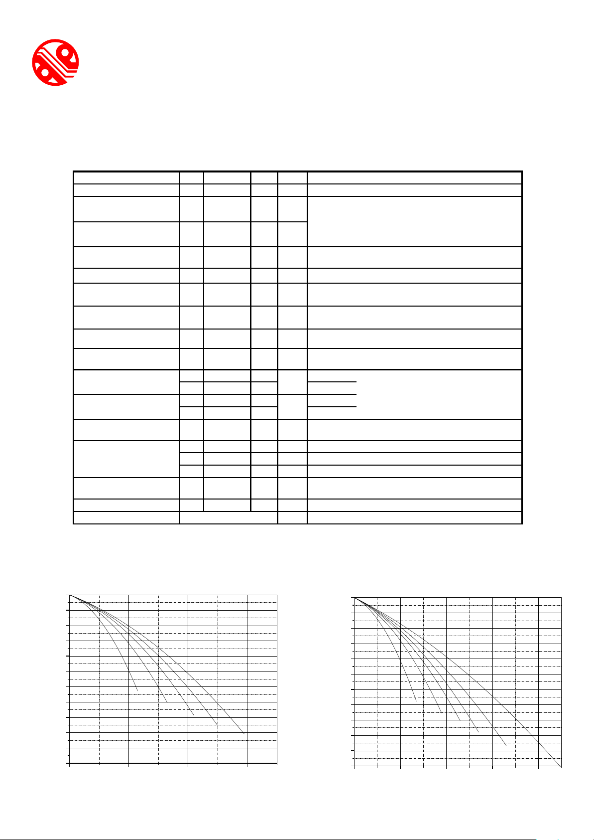
Fig. 1 - Current Ratings Characteristics
Fig. 2 - Current Ratings Characteristics
Page 3

AEGIS
0 100 200 300 400 500
0
1000
2000
3000
4000
5000
180º
120º
90º
60º
30º
*Sinusoidal wavefor m
Maximum Average Forward Power Loss
Maximum Average Forward Power Loss (W)
Average Forward Current (A)
0 100 200 300 400 500
0
500
1000
1500
2000
2500
3000
3500
4000
DC
180º
120º
90º
60º
30º
*Rectangular wavefor m
Maximum Average Forward Power Loss
Maximum Average Forward Power Loss (W)
Average Forward Current (A)
0.5 1.0 1.5 2.0 2.5 3.0 3.5 4.0 4.5 5.0
100
1000
10000
125ºC
25ºC
Forward Voltage Drop
Instantaneous Forward Current (A)
Instantaneous Forward Voltage (V)
10
-3
10
-2
10
-1
10
0
10
1
10
-2
10
-1
10
0
Transient Thermal Impedance Z
thJC
Transient Thermal Impedance Z
thJC
(ºC/W)
Time (s)
SEMICONDUTORES LTDA.
A5N:300.XXH
Fig. 3 - Forward Power Loss Characteristics
Fig. 5 - Forward Voltage Drop Characteristics
Fig. 4 - Forward Power Loss Characteristics
Fig. 6 - Transient Thermal Impedance
Characteristics
Page 4

1E-3 0.01 0.1 1 10 100 1000
0.1
1
10
100
(b)
(a)
T
J
= -40ºC
T
J
= 25ºC
T
J
= 140ºC
I
GD
V
GD
Rectangular gat e pulse
a) Recommended load line for
rated di/dt : 20V, 30W;
tr<=0.5ms, tp=>6ms.
b)Recommended load line for
<=30% rated di/dt : 15V, 40W;
tr<=1ms, tp=>6ms.
(1) PGM = 12W, tp = 5ms
(2) PGM = 30W, tp = 2ms
(3) PGM = 60W, tp = 1ms
(4) PGM = 200W, tp = 300ms
(4)(3)(2)(1)
Gate Characteristics
Instantaneous Gate Voltage (V)
Instantaneous Gate Current (A)
AEGIS
SEMICONDUTORES LTDA.
A5N:300.XXH
Fig. 7 - Gate Trigger Characteristics
Fig. 8 - Outline Characteristics
TO-200AA
 Loading...