

Page 1
1
C
1
2
C
2
DETECT
STROBE
+ SUPPLY V
HORN
3
4
5
6
IRED
7
I / O
89
1
Data Sheet
26110.10A
5358
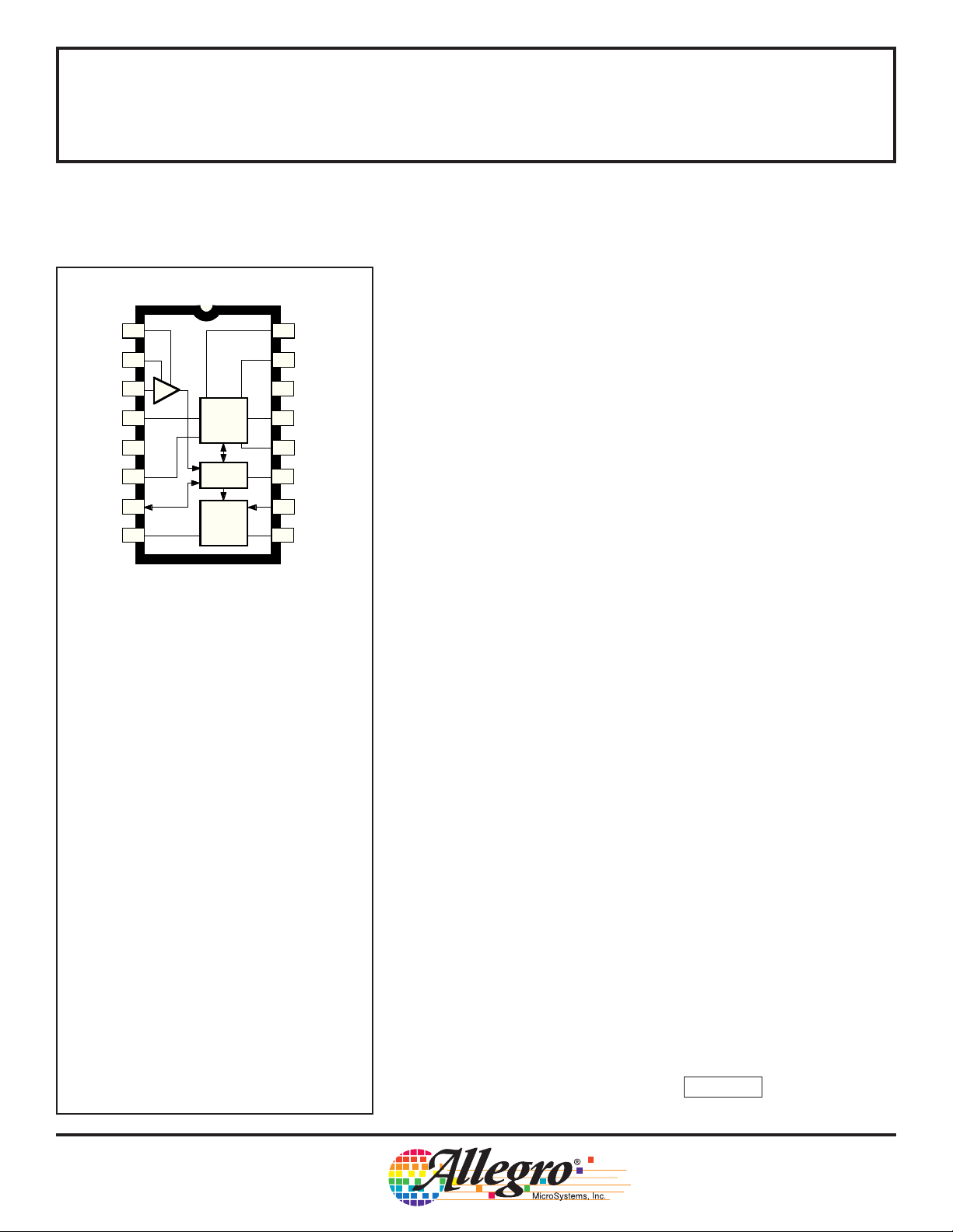
PHOTOELECTRIC SMOKE DETECTOR
WITH INTERCONNECT AND TIMER
The A5358CA is a low-current BiCMOS circuit providing all of the
required features for a photoelectric type smoke detector. This device
can be used in conjunction with an infrared photoelectric chamber to
16
TEST
HUSH
15
V
OSC. &
TIMING
DD
LOGIC
HORN
DRIVER
SS
– SUPPLY
14
TIMING RES.
13
OSC. CAP.
12
11
LED
10
FEEDBACK
HORN
Dwg. PC-007
2
sense scattered light from smoke particles. Special features are
incorporated in the design to facilitate calibration and testing of the
finished detector. The device is designed to comply with Underwriters
Laboratories Specification UL217 and British Standard BS 5446,
Part 1.
A variable-gain photo amplifier can be directly interfaced to an
infrared emitter/detector pair. The amplifier gain levels are determined
by two external capacitors that are then internally selected depending
on the operating mode. Low gain is selected during standby and timer
modes. During a local alarm this low gain is increased (internally) by
~10% to reduce false triggering. High gain is used during the pushbutton test and during standby to periodically monitor the chamber
sensitivity.
The internal oscillator and timing circuitry keeps standby power to
a minimum by sensing for smoke every 10 seconds in a 10 µs window.
A special three-stage speedup sensing scheme is incorporated to
minimize the time to an audible alarm and also to reduce false triggering. Also, two consecutive cycles of degraded chamber sensitivity are
required for a warning signal to occur.
ABSOLUTE MAXIMUM RATINGS
(Voltages are referenced to VSS)
Supply Voltage Range,
VDD.................................... -0.5 V to +15 V
Input Voltage Range,
VIN............................ -0.3 V to V
Input Current, IIN................................... 10 mA
Operating Temperature Range,
TA..................................... -25°C to +75°C
Storage Temperature Range,
TS................................... -55°C to +125°C
CAUTION: CMOS devices have input static
protection but are susceptible to damage if exposed
to extremely high static electrical charges.
+ 0.3 V
DD
The A5358CA is supplied in a low-cost 16-pin dual in-line plastic
package. It is rated for continuous operation over the temperature
range of -25°C to +75°C.
FEATURES
■ Interconnect Up to 50 Detectors
■ Piezoelectric Horn Driver
■ All Internal Low-Battery Detection
■ Power-ON Reset
■ Internal Timer & Control for Reduced Sensitivity
■ Built-In Circuits to Reduce False Triggering
■ 6 V to 12 V Operating Voltage Range
■ ESD-Protection Circuitry on All Pins
Always order by complete part number: A5358CA .
Page 2

5358
PHOTOELECTRIC SMOKE DETECTOR
with INTERCONNECT and TIMER
FUNCTIONAL BLOCK DIAGRAM
DETECT
STROBE
+ SUPPLY
9 V
3
C1
1
C2
2
4
6IRED
– SUPPLY
14
V
SS
V
DD
5
BAND-GAP
REFERENCE
+
–
LOW BATTERY
PHOTO AMP
+
–
V
DD
I / O
7
LOGIC
V
DD
15
HUSH
POWER-ON
OSCILLATOR
& TIMING
RESET
16
TEST
FEEDBACK
10
9
HORN
2
8
HORN
1
11
LED
TIMING RES.
13
12
OSC. CAP.
+V
+V
Dwg. FC-006
115 Northeast Cutoff, Box 15036
Worcester, Massachusetts 01615-0036 (508) 853-5000
Copyright © 1995, 1996 Allegro MicroSystems, Inc.
Page 3

5358
PHOTOELECTRIC SMOKE DETECTOR
with INTERCONNECT and TIMER
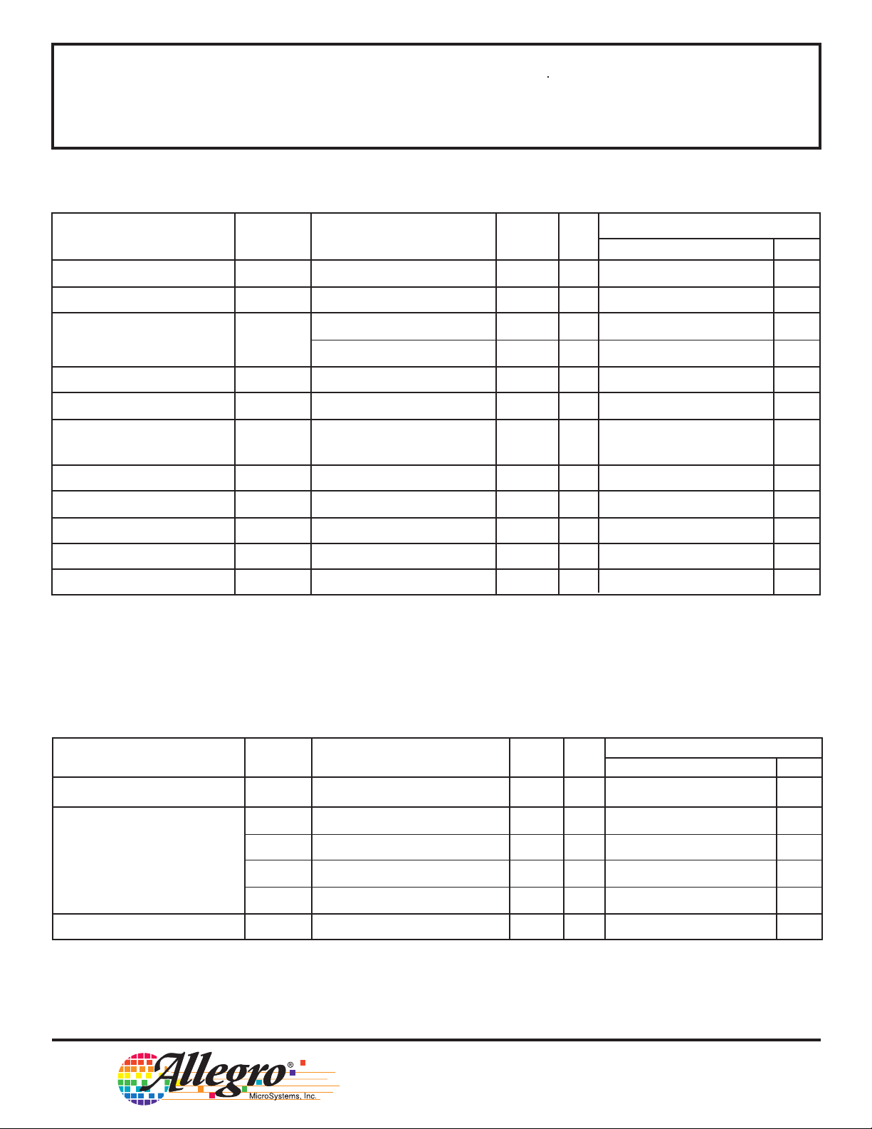
DC ELECTRICAL CHARACTERISTICS at T
= -25°C to +75°C*, V
A
(unless otherwise noted).
Test Limits
Characteristic Symbol Test Conditions Pin V
Supply Voltage Range V
Operating Supply Current I
Low-Level Input Voltage V
High-Level Input Voltage V
DD
DD
IH
Average Standby 5 12 – – 12 µA
Configured per Figure 1
During Strobe ON, I
OFF, 5 12 – – 2.0 mA
RED
Configured per Figure 1
During Strobe ON, I
ON, 5 12 – – 3.0 mA
RED
Configured per Figure 1
IL
5 – 6.0 – 12 V
79––1.5V
10 9 – – 2.7 V
16 9 – – 7.0 V
15 9 – – 0.5 V
793.2––V
10 9 6.3 – – V
16 9 8.5 – – V
15 9 1.6 – – V
= 0 V, in typical application
SS
Min. Typ. Max. Units
DD
Input Leakage High I
Input Leakage Low I
Input Pull-Down Current I
Low-Level Output Voltage V
High-Level Output Voltage V
Strobe Output Voltage V
IH
IL
IN
OL
OH
ST
VIN = VDD, Strobe Active, 1, 2 12 – – 100 nA
Pin 12 @ V
V
= V
IN
V
= VST, Strobe Active, 1, 2, 3 12 – – -100 nA
IN
Pin 12 @ V
V
= V
IN
DD
SS
DD
3, 10, 12 12 – – 100 nA
DD
10, 12 12 – – -100 nA
15, 16 12 – – -1.0 µA
V
= V
IN
DD
No Local Smoke, V
No Local Smoke, V
= V
IN
DD
= 17 V 7 12 – – 140 µA
IN
16, 15 9 0.25 – 10 µA
7920–80µA
IO = 10 mA 11 6.5 – – 0.6 V
= 16 mA 8, 9 6.5 – – 1.0 V
I
O
= 5 mA 13 6.5 – 0.5 – V
I
O
IO= -16 mA 8, 9 6.5 5.5 – – V
Inactive IO = -1 µA412
Active, I
= 100 µA to 500 µA4 9
O
VDD - 0.1
VDD - 5.25
––V
–
VDD - 4.75
V
Continued...
Page 4
5358
PHOTOELECTRIC SMOKE DETECTOR
with INTERCONNECT and TIMER
DC ELECTRICAL CHARACTERISTICS, continued
Test Limits
Characteristic Symbol Test Conditions Pin V
Line Regulation ∆V
ST(∆VDD)
Strobe Temperature Coeff. α
Output Voltage V
I
RED
Line Regulation ∆V
Temperature Coefficient α
I
RED
IRED(∆VDD)
High-Level Output Current I
OFF Leakage Current High I
OFF Leakage Current Low I
Low V
Alarm Threshold V
DD
Common Mode Voltage V
Smoke Comparator Ref. Volt. V
ST
IRED
IRED
OH
OZ
OZ
DD(th)
IC
REF
Active, V
VDD = 6 V to 12 V 4 – – 0.01 – %/°C
Inactive IO = 1 µA, TA = +25°C 6 12 – – 0.1 V
Active I
Active, VDD = 6 V to 12 V 6 – -35 – dB
VDD = 6 V to 12 V 6 – – +0.40 – %/°C
VDD = Alarm, I/O active, 7 9 -4.0 – – mA
V
= VDD - 2 V
O
VO = V
VO = V
Any Alarm Condition 1, 2, 3 Any Alarm Condition Internal -
= 6 V to 12 V 4 – – -60 – dB
DD
= -6 mA, TA = +25°C 6 9 2.85 3.1 3.35 V
O
DD
SS
11, 13 12 – – 1.0 µA
11, 13 12 – – -1.0 µA
5 - 6.9 7.2 7.5 V
Min. Typ. Max. Units
DD
VDD - 4
VDD - 3.7
–
–
VDD - 2
VDD - 3.3
V
V
* Limits over the operating temperature range are based on characterization data.
Characteristics are production tested at +25°C only.
Typical values are at +25°C and are given for circuit design information only.
AC ELECTRICAL CHARACTERISTICS at T
= -25°C to +75°C*, V
A
(unless otherwise noted).
Test Limits
Characteristic Symbol Test Conditions Pin V
Oscillator Period t
Led Pulse Period t
Led Pulse Width t
osc
led1
t
led4
t
led6
t
led7
w(led)
No Local or Remote Smoke 11 9 39 – 48 s
Remote Smoke Only 11 9 None – – –
Local Smoke or Test 11 9 0.60 0.67 0.74 s
Timer Mode, No Alarm 11 9 9.67 10.8 11.8 s
12 9 9.4 10.5 11.5 ms
11 9 9.5 – 11.5 ms
= 0 V, in typical application
SS
DD
Min. Typ. Max. Units
Continued...
115 Northeast Cutoff, Box 15036
Worcester, Massachusetts 01615-0036 (508) 853-5000
Page 5

5358
PHOTOELECTRIC SMOKE DETECTOR
with INTERCONNECT and TIMER
AC ELECTRICAL CHARACTERISTICS, continued.
Test Limits
Characteristic Symbol Test Conditions Pin V
Strobe Pulse Period t
st1
t
st2
t
st3
No Local or Remote Smoke 4 9 9.6 – 11.9 s
After 1 of 3 Valid Samples 4 9 2.42 2.70 2.96 s
After 2 of 3 Valid Samples 4 9 1.21 1.34 1.47 s
and During Local Alarm
DD
Min. Typ. Max. Units
Strobe Pulse Width t
Pulse Period t
I
RED
Pulse Width t
I
RED
Rise Time t
I
RED
Fall Time t
I
RED
I/O to Active Delay t
Rising Edge on I/O to Alarm t
Horn Warning Pulse Period t
t
st4
t
st5
t
st6
w(st)
ired1
t
ired2
t
ired3
t
ired4
t
ired5
t
ired6
w(ired)
r(ired)
f(ired)
d(io)
r(io)
horn
Remote Alarm 4 9 9.67 10.8 11.8 s
Chamber Test or Low Supply 4 9 38.9 – 47.1 s
Test, No Local Alarm
Pushbutton Test, No Alarm 4 9 300 336 370 ms
4 9 9.5 – 11.5 ms
No Local or Remote Smoke 6 9 9.6 – 11.9 s
After 1 of 3 Valid Samples 6 9 2.42 2.70 2.96 s
After 2 of 3 Valid Samples 6 9 1.21 1.34 1.47 s
and During Local Alarm
Remote Alarm 6 9 9.67 10.8 11.8 s
Chamber Test, No Local Alarm 6 9 38.9 – 47.1 s
Pushbutton Test, No Alarm 6 9 300 336 370 ms
6 9 94 – 116 µs
10% to 90% 6 – – 30 µs
90% to 10% 6 – – 200 µs
Local Alarm 7 9–0–s
No Local Alarm 7 9 – – 1.34 s
Low Supply and Degraded 8, 9 9 38.9 – 47.1 s
Chamber Sensitivity
Horn Warning Pulse Width t
w(horn)
Low Supply and Degraded 8, 9 9 9.5 – 11.5 ms
Chamber Sensitivity
Horn ON Time t
Horn OFF Time t
on(horn)
off(horn)
Local or Remote Alarm 8, 9 9 – 252 – ms
Local or Remote Alarm 8, 9 9 – 84 – ms
* Limits over the operating temperature range are based on characterization data.
Characteristics are production tested at +25°C only.
Typical values are at +25°C and are given for circuit design information only.
Page 6

5358
PHOTOELECTRIC SMOKE DETECTOR
with INTERCONNECT and TIMER
PIN AND CIRCUIT DESCRIPTION
(In Typical Application)
PIN 1 (C1)
A capacitor connected to this pin determines the gain
of the photo amplifier during the push-to-test mode and
during the chamber monitor test. A typical value for this
high-gain mode is 0.047 µF but should be selected
based on the photo chamber background reflections
reaching the detector and the desired level of sensitivity.
Ae ≈ 1+(C1/10) where C1 is in pF. Ae should not
exceed 10 000.
PIN 2 (C2)
A capacitor connected to this pin determines the gain
of the photo amplifier during standby. A typical value for
this low-gain mode is 4700 pF but should be selected
based on a specific photo chamber and the desired level
of sensitivity to smoke. Ae ≈ 1+(C2/10) where C2 is in pF.
Ae should not exceed 10 000. This gain increases by a
nominal 10% after a local alarm is detected (three consecutive detections). Coupling of other signals to C
(C1 and the DETECT inputs also) must be minimized.
A resistor must be installed in series with C2.
PIN 3 (DETECT)
This is the input to the photo amplifier and is connected to the cathode of the photo diode. The photo
diode is operated at zero bias and should have low darkleakage current and low capacitance.
PIN 4 (STROBE)
This output provides a strobed, regulated voltage of
V
– 5 V. The minus side of all internal and external
DD
photo amplifier circuitry is referenced to this pin.
2
PIN 5 (VDD)
This pin is connected to the most-positive supply
potential and can range from 6 V to 12 V with respect
to VSS.
PIN 6 (I
This output provides a pulsed base current for the
external npn transistor, which drives the IR emitter. Its
beta should be greater than 100. The I
active, to minimize noise impact, when the horn and
visible LED outputs are active.
PIN 7 (I/O)
A connection at this pin allows multiple smoke detectors to be interconnected. If a local smoke condition
occurs, this pin is driven high. As an input, this pin is
sampled nominally every 1.35 seconds during standby.
Any local-alarm condition causes this pin to be ignored as
an input.
This pin has an on-chip pull-down resistor and must
be left unconnected if not used. In application, there is a
series current-limiting resistor to other smoke alarms.
PIN 8 (HORN1)
PIN 9 (HORN2)
PIN 10 (FEEDBACK)
These three pins are used in conjunction with external
passive components and a self-resonating piezoelectric
transducer. HORN1 is connected to the piezo metal
support electrode; the complementary output, HORN2, is
connected to the ceramic electrode and the FEEDBACK
input to the feedback electrode.
RED
)
output is not
RED
A continuous modulated tone indicates either a local
or remote alarm condition. A short (10 ms) chirp indicates
a low-battery condition or degraded chamber sensitivity.
The low-battery chirp occurs almost simultaneous with the
visible LED flash. If the FEEDBACK pin is not used, it
must be connected to VDD or VSS.
115 Northeast Cutoff, Box 15036
Worcester, Massachusetts 01615-0036 (508) 853-5000
Continued...
Page 7

5358
PHOTOELECTRIC SMOKE DETECTOR
with INTERCONNECT and TIMER
PIN AND CIRCUIT DESCRIPTION, continued
PIN 11 (LED)
This open-drain NMOS output is used to directly drive
a visible LED. The load for the low-battery test is applied
to this output. The low-battery test does not occur coincident with any other test or alarm signal. The LED also
indicates detector status as follows (with component
values as in the typical application, all times nominal):
Standby - Pulses every 43 seconds.
Local Smoke - Pulses every 0.67 second.
Remote Alarm - No pulses.
Test Mode - Pulses every 0.67 second.
Timer Mode - Pulses every 10 seconds.
PIN 12 (OSC. CAP.)
A capacitor between this pin and VDD, along with a
parallel resistor, forms part of a two-terminal oscillator and
sets the internal clock low time. With component values
as shown, this nominal time is 11 ms and essentially the
oscillator period.
PIN 13 (TIMING RES.)
A resistor between this pin and OSC. CAP. (pin 12) is
part of the two-terminal oscillator and sets the internal
clock high time, which is also the I
component values as shown, this nominal time is 105 µs.
pulse width. With
RED
cycle, I
gain is increased by internal selection of C1. Background
reflections in the smoke chamber can be used to simulate
a smoke condition. After the third I
test (three consecutive simulated smoke conditions)
activates the horn drivers and the I/O pin. When the
push-button is released, the input returns to VSS due to
the internal pull down. After one oscillator cycle, the
amplifier gain returns to normal and after three additional
I
RED
mode and returns to standby. This high-to-low transition
on pin 16 also resets and starts the 10 minute hush timer
(timer mode).
Pin Name Pin No. Configuration
I/O 7 Disabled as an output. A logic
pulses every 336 ms (nominal) and amplifier
RED
pulse, a successful
RED
pulses (less than one second), the device exits this
high on this pin places the photo
amplifier output on pin 1 or pin 2
as determined by pin 15. The
amplifier output appears as
pulses.
PIN 14 (VSS)
This pin is connected to the most negative supply
potential (usually ground).
PIN 15 (HUSH)
This input pin serves two purposes in normal operation. It serves as an enable for the internal 10-minute
(nominal) timer and also as the reference for the smoke
comparator during the timer mode. This reference is
established by a resistive divider between VDD and
STROBE (RX1 and RX2). This allows the detector to have
a different sensitivity set point during the timer mode. If
the timer mode is not used, this pin can be left open or
connected to VSS, which disables this mode.
PIN 16 (TEST)
This pin has an internal pull-down device and is used
to manually invoke two test modes and a Timer Mode.
The Push-to-Test Mode is initiated by a high logic
level on this pin (usually the depression of a normally
open push-button switch to VDD). After one oscillator
HUSH 15 If the I/O pin is high, this pin
controls the amplifier gain capaci
tor. If pin 15 is low, normal gain is
selected and the amplifier output
is on pin 1. If pin 15 is high,
supervisory gain is selected and
the amplifier output is on pin 2.
FEEDBACK 10 If pin 7 is high and pin 15 is low
(normal gain), taking this pin to a
high logic level increases the
amplifier gain by ~10% (hysteresis).
OSC. CAP. 12 This pin may be driven by an
external clock source. Driving
this pin low and high drives the
internal clock low and high. The
external RC network may remain
intact.
Page 8

5358
PHOTOELECTRIC SMOKE DETECTOR
with INTERCONNECT and TIMER
PIN AND CIRCUIT DESCRIPTION, continued
The Diagnostic Test Mode is initiated by pulling this
pin below VSS and continuously sourcing 400 µA from the
pin for at least one clock cycle on the OSC. CAP. pin.
This mode is used to facilitate calibration and test of the IC
and the assembled detector. In this mode, certain device
pins are reconfigured as described below. In this mode,
the I
pulse rate is increased to one every OSC. CAP.
RED
cycle and the STROBE pin is always active. To exit this
mode, the test pin is floated for at least one OSC. CAP.
cycle.
TYPICAL APPLICATION
CONNECT FOR TIMER MODE OR "HUSH" OPERATION
V
DD
X1
R
X2
R
8.2kΩ
5kΩ
4.7kΩ
SMOKE
CHAMBER
C
1
1
C
2
560Ω
200kΩ
2
3
4
5
V
DD
Pin Name Pin No. Configuration
HORN
1
8 This pin is reconfigured as the
smoke integrator output. Three
consecutive smoke detections
will cause this pin to go high
and three consecutive nosmoke detections cause this
pin to go low.
LED 11 This pin becomes a low-battery
indicator. The open-drain
NMOS output is normally OFF.
If V
falls below the low-
DD
battery threshold, the output
turns ON.
CONNECT FOR
NON-TIMER MODE
OPERATION
+
22µF
10MΩ
9 V
330Ω
OSC. &
TIMING
PUSH
TO
TEST
16
15
V
14
SS
1500pF
13
100kΩ
12
1kΩ
TO/FROM
OTHER
UNITS
100µF
+
22Ω
220Ω
6
7
8 9
115 Northeast Cutoff, Box 15036
Worcester, Massachusetts 01615-0036 (508) 853-5000
LOGIC
HORN
DRIVER
11
1000pF 220kΩ
10
100kΩ
Dwg. EC-006
Page 9

5358
PHOTOELECTRIC SMOKE DETECTOR
with INTERCONNECT and TIMER
STANDBY TIMING DIAGRAM
(not to scale)
OSC. CAP
(PIN 12)
t
osc
INTERNAL
CLOCK
IRED
(PIN 6)
t
ired
t
w(ired)
STROBE
(PIN 4)
LED
(PIN 11)
SAMPLE
SMOKE
HORN
ENABLE
t
w(st)
t
w(led)
NO LOW SUPPLY
CHAMBER SENSITIVITY NORMAL
t
st
WARNING
CHIRP
t
led
t
horn
LOW SUPPLY OR
DEGRADED SENSITIVITY
WARNING CHIRPS ARE OFFSET
Dwg. WC-008
t
w(horn)
Page 10

5358
PHOTOELECTRIC SMOKE DETECTOR
with INTERCONNECT and TIMER
LOCAL ALARM TIMING DIAGRAM
(not to scale)
t
w(ired)
10%
IRED
(PIN 6)
t
ired3
90%
t
f(ired)
10%
t
ired4
t
ired6
STROBE
(PIN 4)
LED
(PIN 11)
I/O
(PIN 7)
HORN
ENABLE
t
st3
t
w(led)
LOCAL SMOKE
(REMOTE SMOKE =
DON'T CARE)
t
w(st)
t
led1
tt
on(horn)
NO SMOKE
3RD STROBE WITH SMOKE
off(horn)
3RD STROBE WITHOUT SMOKE
t
t
st4
(NO PULSES)
r(io)
REMOTE SMOKE
(NO LOCAL SMOKE)
t
st6
t
led6
(AS OUTPUT)(AS INPUT)(AS OUTPUT)
tt
on(horn) off(horn)
TEST
Dwg. WC-009
115 Northeast Cutoff, Box 15036
Worcester, Massachusetts 01615-0036 (508) 853-5000
Page 11

5358
PHOTOELECTRIC SMOKE DETECTOR
with INTERCONNECT and TIMER
Dimensions in Inches
(controlling dimensions)
16
0.280
0.240
0.014
9
0.008
0.300
BSC
0.430
MAX
0.210
MAX
7.11
6.10
0.015
MIN
1
0.070
0.045
16
1
1.77
1.15
0.022
0.014
8
0.775
0.100
BSC
0.735
Dimensions in Millimeters
(for reference only)
9
8
19.68
18.67
2.54
BSC
0.005
MIN
0.150
0.115
0.13
MIN
0.355
0.204
Dwg. MA-001-16A in
10.92
MAX
7.62
BSC
5.33
MAX
0.39
MIN
0.558
0.356
NOTES: 1. Lead thickness is measured at seating plane or below.
2. Lead spacing tolerance is non-cumulative.
3. Exact body and lead configuration at vendor’s option within limits shown.
3.81
2.93
Dwg. MA-001-16A mm
Page 12

5358
PHOTOELECTRIC SMOKE DETECTOR
with INTERCONNECT and TIMER
SAFETY & SECURITY ICs
SELECTION GUIDE
Part
Number Function
A3054KU/SU Multiplexed Two-Wire Hall-Effect Sensor
A5347CA Ionization-Type Smoke Detector with Interconnect and Timer
A5348CA Ionization-Type Smoke Detector with Interconnect, Timer, and Reverse-Battery Protection
A5349CA Ionization-Type Smoke Detector with Interconnect and Timer for AC Line Operation
A5350CA Ionization-Type Smoke Detector with Interconnect and Reverse-Battery Protection
A5358CA Photoelectric-Type Smoke Detector with Interconnect and Timer
Allegro MicroSystems, Inc. reserves the right to make, from time to time, such departures from
the detail specifications as may be required to permit improvements in the design of its products.
The information included herein is believed to be accurate and reliable. However, Allegro
MicroSystems, Inc. assumes no responsibility for its use; nor for any infringements of patents or
other rights of third parties which may result from its use.
115 Northeast Cutoff, Box 15036
Worcester, Massachusetts 01615-0036 (508) 853-5000
 Loading...