

Page 1
1
查询A500K050-BG272供应商
Advanced v.3
ProASIC
Features and Benefits
High Capacity
• 98,000 to 1.1 Million System Gates
• 14k to 138k Bits of Two-Port SRAM
• 210 to 623 User I/Os
Performance
• 33 MHz PCI 32-Bit
• Internal System Performance up to 250 MHz
• External System Performance up to 100 MHz
Low Power
• Low Impedance Flash Switches
• Segmented Hierarchical Routing Structure
• Small Efficient Logic Cells
High Performance Routing Hierarchy
• Ultra Fast Local Network
• Efficient Long Line Network
• High Speed Bus Network
• High Performance Global Network
Nonvolatile and Reprogrammable Flash
Technology
• Live at Power-Up
• No Configuration Boot Device Required
• Retains Programmed Design During Power-Down/
Power-Up Cycles
500K Family
™
I/O
• Mixed 2.5/3.3 Volt Support
• 3.3V, 33 MHz PCI Compliance (PCI Revision 2.2)
• Individually Selectable 2.5V or 3.3V I/Os and Slew Rate
(25, 50, and 100 mA/nsec)
Secure Programming
• Security Bit Prevents Read Back of Programming Bit
Stream
Standard FPGA and ASIC Design Flow
• Flexibility to Choose Vendor-Specific Front-End Tools
• Provide Efficient Design Through Front-End Timing and
Gate Optimization
ISP Support
• In-System Programming (ISP) with Silicon Sculptor and
Silicon Explorer II
Embedded Memory Netlist Generator for
SRAMs and FIFOs
• Ensures Optimal Usage of Embedded Memory Blocks
• Up to 133 MHz Synchronous and Asynchronous Operation
JTAG Support
• IEEE Std. 1149.1 (JTAG) Compliant
Individual ProASIC Device ID
• Control and Restrict IP Delivery to Individual ProASIC
Device
ProASIC Product Profile
Device A500K050 A500K130 A500K180 A500K270 A500K350 A500K440 A500K510
Maximum System Gates
Typical Gates
Maximum Flip-Flops
Embedded RAM Bits
Embedded RAM Blocks (256 X 9)
Logic Tiles
Global Clocks
Maximum User I/Os
JTAG
PCI
Package (by Pin Count)
PQFP
PBGA
FBGA
December 1999
© 1999 Actel Corporation
98,000 287,000 369,000 473,000 638,000 956,000 1,100,000
43,000 105,000 150,000 215,000 280,000 350,000 410,000
5,376 12,800 18,432 26,880 34,816 43,776 51,200
14k 46k 55k 65k 74k 124k 138k
6 202428325460
5,376 12,800 18,432 26,880 34,816 43,776 51,200
4444444
210 312 368 446 496 570 623
Yes Yes Yes Yes Yes Yes Yes
Yes Yes Yes Yes Yes Yes Yes
208
272
208
272, 456
208
456
580
208
456
580 580 580 580
Page 2
General Description
The ProASIC 500K family combines the advantages of ASICs
with the benefits of programmable devices through its
nonvolatile Flash technology. ProASIC 500K devices make it
possible to create high-density systems using existing ASIC or
FPGA design flows and tools, shortening time-to-production.
ASIC migration is not necessary for any volume because the
family offers cost effective reprogrammable solutions, ideal
for applications in the networking, telecom, computer, and
consumer markets.
The ProASIC 500K family offers seven devices with 98k to
1.1M system gates and includes up to 138k bits of embedded
Ordering Information
A500K130 – PQ 2081
two-port memory. These memory blocks include hardwired
FIFO circuitry as well as circuits to generate or check parity.
This minimizes external logic gate count and complexity
while maximizing flexibility and utility.
Process Technology
The ProASIC 500K family achieves its non-volatility and
reprogrammability through an advanced 4LM Flash-based
0.25µ channel length LVCMOS technology process. Standard
CMOS design techniques are used to implement logic and
control functions resulting in highly predictable performance
and gate array compatibility.
Package Lead Count
Package Type
BG = Ball Grid Array
PQ = Plastic Quad Flat Pack
FG = Fine Ball Grid Array
Speed Grade
Blank = Standard Speed
–1 = TBD
Part Number
A500K050 = 98,000 System Gates
A500K130 = 287,000 System Gates
A500K180 = 369,000 System Gates
A500K270 = 473,000 System Gates
A500K350 = 638,000 System Gates
A500K440 = 956,000 System Gates
A500K510 = 1,100,000 System Gates
Application (Ambient Temperature Range)
Blank = Commercial (0 to +70°C)
I = Industrial (–40 to +85°C)
PP = Pre-production
ES = Engineering Silicon (Room Temperature Only)
2
Page 3
✔
✔
✔
✔
✔
✔
Product Plan
A500K050 Device
208-Pin Plastic Quad Flat Pack (PQFP)
272-Pin Plastic Ball Grid Array (PBGA)
A500K130 Device
™
ProASIC
500K Family
Speed Grade Application
Std –1* C I
✔
✔
PPP
PPP
208-Pin Plastic Quad Flat Pack (PQFP)
272-Pin Plastic Ball Grid Array (PBGA)
456-Pin Plastic Ball Grid Array (PBGA)
✔
PPP
PPP
PPP
A500K180 Device
208-Pin Plastic Quad Flat Pack (PQFP)
456-Pin Plastic Ball Grid Array (PBGA)
PPP
PPP
580-Pin Fine Ball Grid Array (FBGA) P P P P
A500K270 Device
208-Pin Plastic Quad Flat Pack (PQFP)
456-Pin Plastic Ball Grid Array (PBGA)
PPP
PPP
580-Pin Fine Ball Grid Array (FBGA) P P P P
A500K350 Device
580-Pin Fine Ball Grid Array (FBGA) P P P P
A500K440 Device
580-Pin Fine Ball Grid Array (FBGA) P P P P
A500K510 Device
580-Pin Fine Ball Grid Array (FBGA) P P P P
Contact your Actel sales representative for package availability.
Applications: C = Commercial Availability:
✔
= Limited Availability. Contact your Actel Sales representative for the latest
I = Industrial availability information.
*Speed Grade: –1 = TBD P = Planned
Plastic Device Resources
User I/Os
Device
208-Pin
A500K050 170 210 — —
A500K130 170 210 312 —
A500K180 170 — 368 368
A500K270 170 — 368 446
A500K350 — — — 496
A500K440 — — — 496
A500K510 — — — 496
Package Definitions (Contact your Actel sales representative for product availability.)
PQFP = Plastic Quad Flat Pack, PBGA = Plastic Ball Grid Array, FBGA = Fine Ball Grid Array
PQFP
PBGA
272-Pin
PBGA
456-Pin
FBGA
580-Pin
3
Page 4
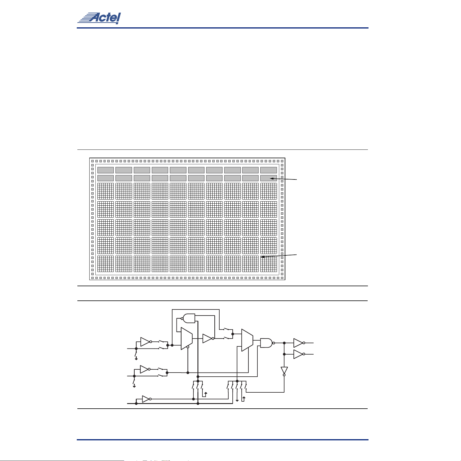
ProASIC 500K Architecture
The ProASIC 500K family utilizes a proprietary architecture
that results in granularity comparable to gate arrays. Unlike
SRAM-based FPGAs, ProASIC devices do not utilize look-up
tables or architectural mapping during design. Instead,
designs are directly synthesized to gates that streamline the
design flow, increase design productivity, and eliminate
dependencies on vendor-specific design tools.
The ProASIC 500K device core consists of a Sea-of-Tiles
™
(Figure 1). Each tile (Figure 2) can be configured into a
3-input logic function (i.e. NAND gate, D-Flip-Flop, etc.) by
programming the appropriate interconnect Flash switches,
shown in Figure 3 on page 5. Gates and larger functions are
connected together, utilizing the four levels of routing
hierarchy. Flash memory bits are distributed throughout each
device providing non-volatile, reconfigurable interconnect
programming. Flash switches are programmed to connect
signal lines to the appropriate logic cell inputs and outputs.
Dedicated high-performance lines are connected as needed
for fast, low-skew clock distribution throughout the core.
Maximum core utilization is possible for virtually any design.
The ProASIC 500K devices also contain embedded two-port
SRAM blocks that have built in FIFO/RAM control logic.
Programming options include synchronous or asynchronous
operation, two-port RAM configurations, user defined depth
and width, and parity generation or checking. Table 2 on
page 9 lists the 24 basic memory configurations.
Figure 1 • The ProASIC Device Architecture
In 1
256x9 Two-Port SRAM
or FIFO Block
Logic Tile
Local Routing
Efficient Long
Line Routing
In 2 (CLK)
In 3 (Reset)
Figure 2 • Core Logic Tile
4
Page 5
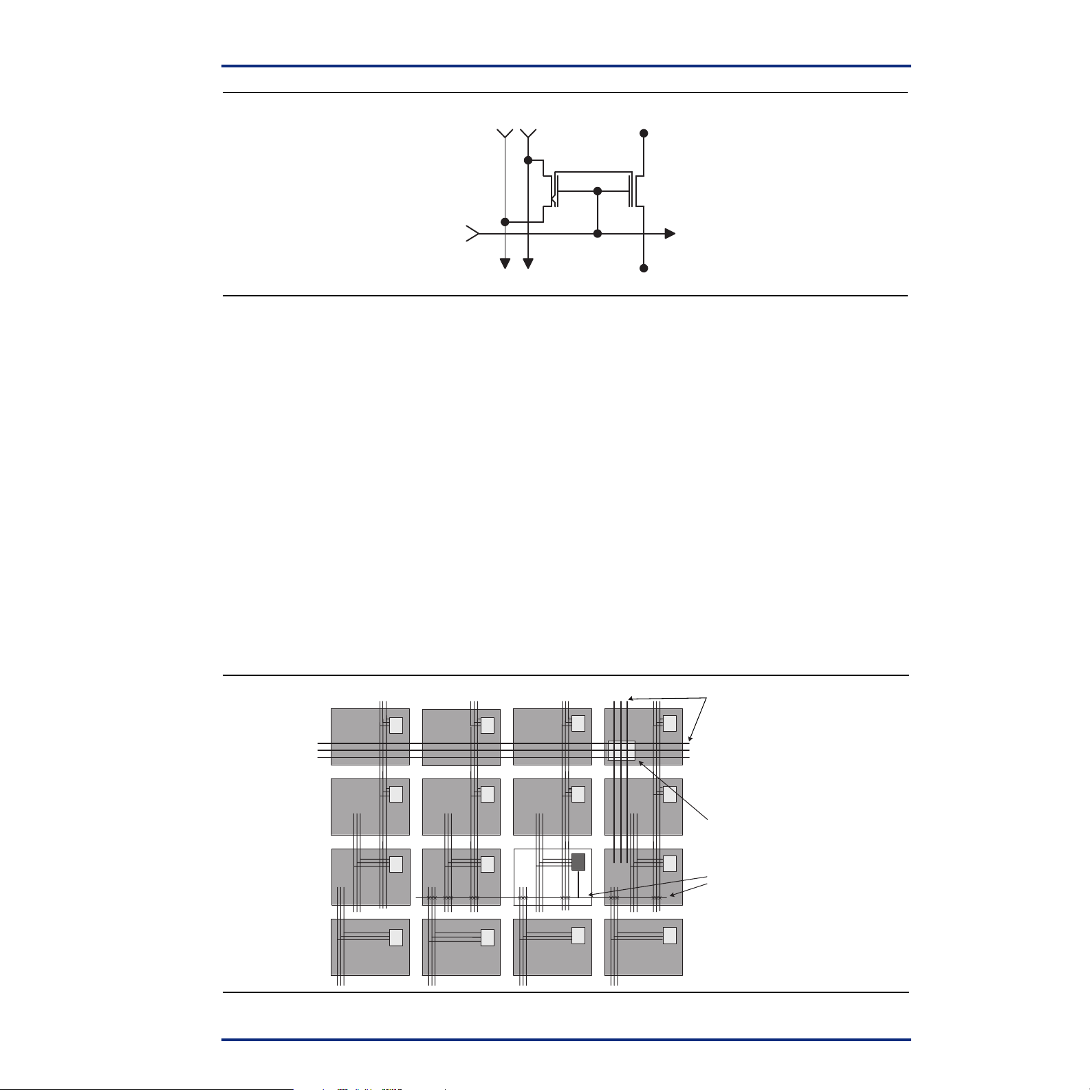
Sel 1 Sel 2
Word
Figure 3 • Flash Switch
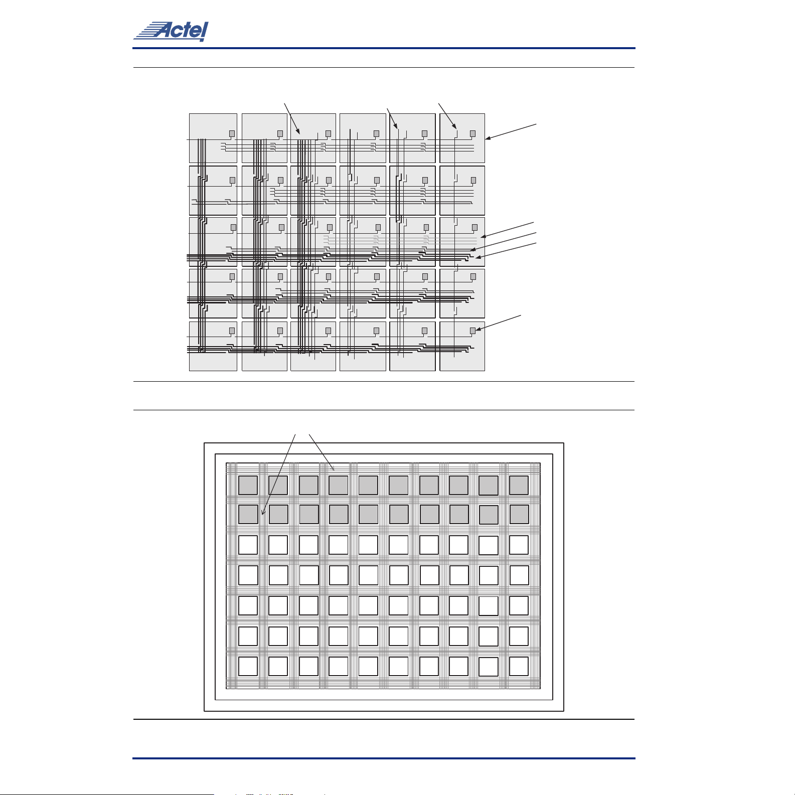
Routing Resources
The routing structure of the ProASIC 500K devices is
designed to provide high performance through routing
flexibility. It is composed of four levels of hierarchical
resources: ultra fast local resources, efficient long line
resources, high speed bus resources, and high performance
global networks.
The ultra fast local resources are high speed dedicated lines
that allow the output of each tile to directly connect to every
input of the eight surrounding tiles (Figure 4).
The efficient long line resources provide routing for longer
distance and higher fanout connections. These resources vary
in length (spanning 1, 2, or 4 tiles), run both vertically and
horizontally, and cover the entire ProASIC device (Figure 5
on page 6). Each tile can drive signals onto the efficient long
line resources, and the resources can access every input of a
tile. Active buffers are inserted automatically by the
ASICmaster software to limit the effects of loading due to
distance and fanout.
™
ProASIC
Switch In
Switch Out
500K Family
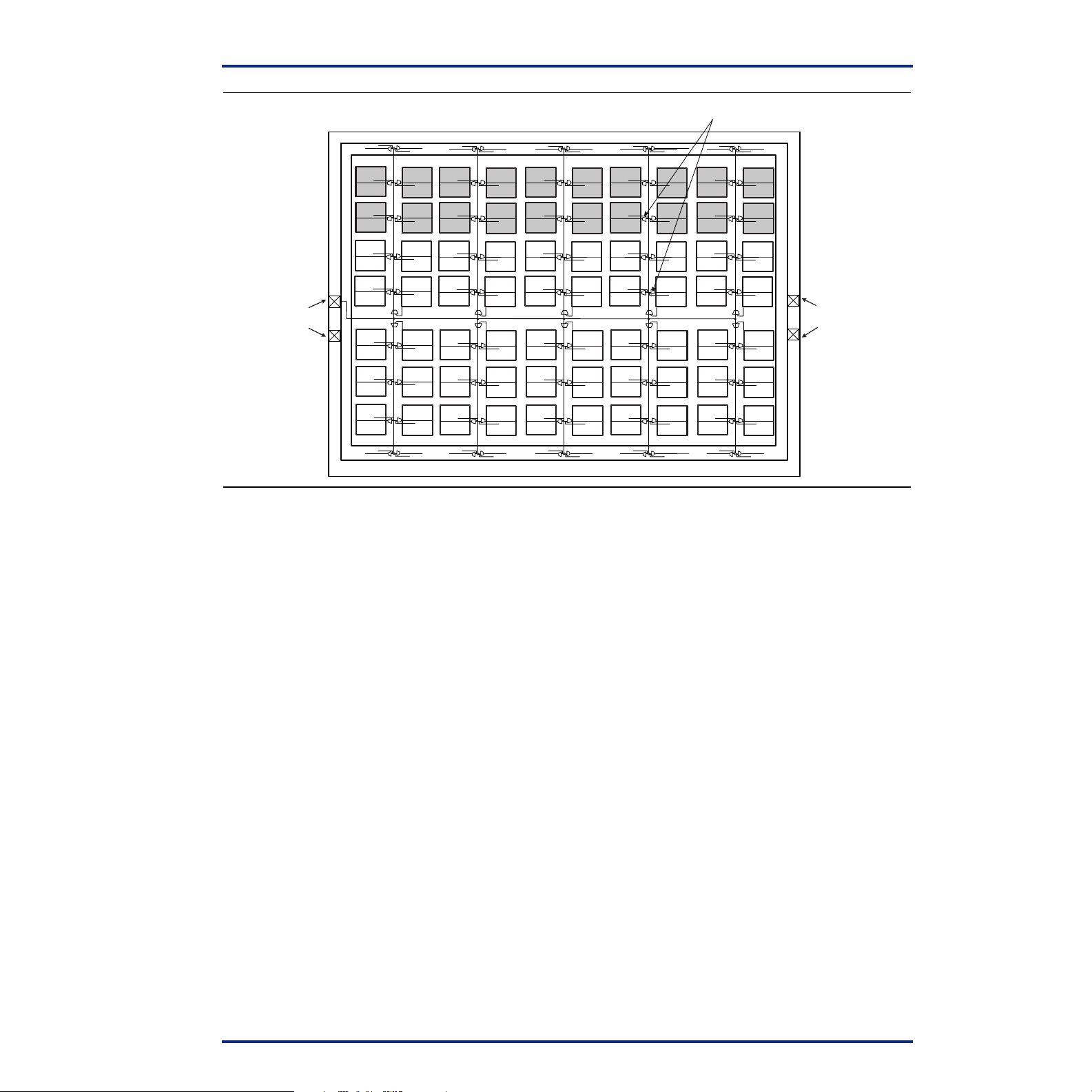
The high speed bus resources span across the entire device
with minimal delay and are used to route very long or very
high fanout nets. These resources run vertically and
horizontally, and provide multiple access to each group of
tiles throughout the device (Figure 6 on page 6).
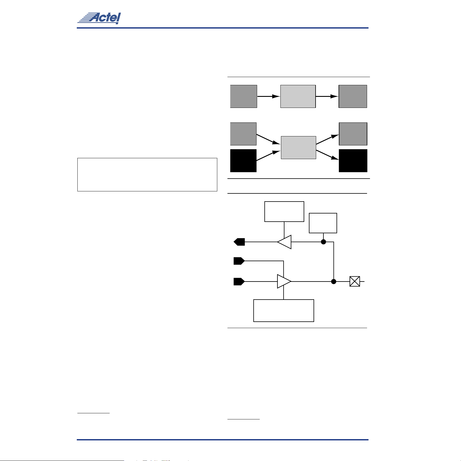
The high performance global networks are low skew, high
fanout nets that are accessible from four dedicated pins or
from internal logic (Figure 7 on page 7). These nets are
typically used to distribute clocks, resets, and other high
fanout nets requiring a minimum skew. The global networks
are implemented as clock trees, and signals can be
introduced at any junction. These can be used hierarchically,
with signals accessing every input on all tiles.
L
L
L
L L
Figure 4 • Ultra Fast Local Resources
Efficient
Long Lines
L
Inputs
L
L
LL
L
Output
L L
L
L
L
(1, 2, or 4 tiles long)
Connection to
logic cell inputs
Ultra Fast
Local Lines
(connects a tile to the
adjacent tile, I/O buffer,
or memory block)
5
Page 6
4 Tiles Long
LL LLLL
LL LLLL
LL LLLL
LL LLLL
LL LLLL
2 Tiles Long
1 Tile Long
Logic Tile
1 Tile Long
2 Tiles Long
4 Tilss Long
Logic Cell
Figure 5 • Efficient Long Line Resources
High Speed Bus Resouces
PAD RING
PAD RING
I/O RING
I/O RING
PAD RING
Figure 6 • High Speed Bus Resources
6
Page 7
PAD RING
PAD RING
ProASIC
High Performace
Global Network
I/O RING
™
500K Family
Global
Pads
I/O RING
PAD RING
Figure 7 • High Performance Global Network
Global
Pads
7
Page 8
Input/Output Blocks
To meet the needs of complex system designs, the ProASIC
500K family offers devices with a large number of I/O pins,
with the A500K510 device offering up to 623 user I/O pins. If
the I/O pad is powered at 3.3V, each I/O can be selectively
configured at 2.5V and 3.3V compliant threshold levels.
Table 1 shows the various supply voltage configurations
available in the ProASIC devices. Figure 8 illustrates I/O
interfaces with other devices. All I/Os also include an ESD
protection circuit. Each I/O is tested according to the
following models:
Human Body Model (HBM)
1500V
(Per Mil Std 883 Method 3015)
Machine Model 200V
Table 1 • ProASIC Power Supply Voltages
V
DDP
Input T olerance
2.5V 3.3V
2.5V 3.3V, 2.5V
• Selectable drive strengths
• Selectable slew rates (25mA/s, 50mA/s, 100mA/s)
• Three-state enable
2.5V
Device
2.5V
Device
3.3V
Device
ProASIC
V
DDL
V
DDP
ProASIC
V
DDL
V
DDP
= 2.5V
= 2.5V
= 2.5V
= 3.3V
2.5V
Device
2.5V
Device
3.3V
Device
Output Drive
Note: V
DDL
is always 2.5V.
2.5V 3.3V, 2.5V
The I/O pads are fully configurable to provide the maximum
flexibility and speed. Each pad can be configured as an input,
an output, a three-state driver, or a bi-directional buffer
(Figure 9). I/O pads configured as inputs have the following
features:
• Individually selectable 2.5V or 3.3V compliant threshold
1
levels
• Optional pull-up resistor
I/O pads configured as outputs have the following features:
• Individually selectable 2.5V or 3.3V compliant output
1
signals
• 3.3V PCI compliant
• Ability to drive LVTTL and LVCMOS levels
• Selectable drive strengths
• Selectable slew rates (25mA/s, 50mA/s, 100mA/s)
• Three-state enable
I/O pads configured as bi-directional buffers have the
following features:
• Individually selectable 2.5V or 3.3V compliant output
signals and threshold levels
1
• 3.3V PCI compliant
• Ability to drive LVTTL and LVCMOS levels
• Optional pull-up resistor
1. If V
= 2.5V, pads are compliant to 2.5V level signals as defined by JEDEC
DDP
JESD 8-5.
Figure 8 • I/O Interfaces
3.3V/2.5V
Signal Control
Y
EN
A
3.3V/2.5V Signal Control
Drive Strength and Slew
Rate Control
Pull-up
Control
Pad
Figure 9 • I/O Block Schematic Representation
User Security and Traceability
2
The ProASIC 500K devices have a read-protect bit that, once
programmed, prevents the programmed contents from being
read from the part. To clear the read-protect bit, the entire
part must be erased. This capability lets you secure the
programmed design and prevent it from being read back and
duplicated. For traceability a 12-character alphanumeric user
part number field allows the user to assign a user part ID,
which can subsequently be read back by the programmer.
2. Available after completion of full qualification/characterization 2H, 2000.
8
Page 9

Embedded Memory Floorplan
The embedded memory is located across the top of the device
(see Figure 1 on page 4). Depending upon the device, 6 to 60
(256x9) blocks of memory are available to support a variety of
possible memory configurations. Each block can be
programmed as an independent memory or combined, using
dedicated memory routing resources, to form larger and more
complex memories.
Embedded Memory Configurations
The embedded memory in the ProASIC 500K family offers
great flexibility in memory configuration. Whereas other
programmable vendors typically provide single port memories
that can be transformed into a two-port memory at the loss of
half the memory, each ProASIC block is designed and
optimized as a two-port memory (1r1w). This provides 138k
total memory bits for two-port and single port memory usage
in the A500K510 device.
Each memory can be configured as a FIFO or SRAM, with
independent selection of synchronous or asynchronous read
and write ports (Table 2). However, multiple write ports are
not supported. Additional characteristics include
programmable FIFO flags and selectable depth, and parity
check and generation. Figure 10 and Figure 11 on page 10
™
ProASIC
500K Family
show the block diagram of the basic SRAM and FIFO blocks.
These memories are designed to operate at up to 133 MHz
when operated individually. Each block contains a 256 word
deep by 9-bit wide (1r, 1w) memory. The memory blocks,
shown in Figure 12 on page 11, may be combined in parallel
to form wider memories or stacked to form deeper memories.
This provides optimal bit widths of 9 (1 block), 18, 36, and 72,
and optimal depths of 256, 572, 768, and 1024. Refer to the
ProASIC Macro Library Guide for more information.
Figure 13 on page 11 shows an example of optimal memory
usage. Three memories have been compiled with various
widths and depths using 10 blocks and consuming all 23,040
bits. Figure 14 on page 11 shows an example of doubling up
memory to create extra read ports. In this example, 10 out of
60 blocks of the A500K510 are fully used, but yield an
effective 6,912 bits of multiple port memories. The
MEMORYmaster
™
software facilitates an easy means of
building wider and deeper memories for optimal memory
usage.
Table 2 • Basic Memory Configurations
Type Write Access Read Access Parity Library Cell Name
RAM Asynchronous Asynchronous Checked RAM256x9AA
RAM Asynchronous Asynchronous Generated RAM256x9AAP
RAM Asynchronous Synchronous T ransparent Chec ked RAM256xAST
RAM Asynchronous Synchronous T ransparent Gener ated RAM256xASTP
RAM Asynchronous Synchronous Pipelined Checked RAM256x9ASR
RAM Asynchronous Synchronous Pipelined Generated RAM256x9ASRP
RAM Synchronous Asynchronous Checked RAM256x9SA
RAM Synchronous Asynchronous Generated RAM256xSAP
RAM Synchronous Synchronous T r ansparent Chec ked RAM256x9SST
RAM Synchronous Synchronous T r ansparent Generated RAM256x9SSTP
RAM Synchronous Synchronous Pipelined Checked RAM256x9SSR
RAM Synchronous Synchronous Pipelined Generated RAM256x9SSRP
FIFO Asynchronous Asynchronous Checked FIFO256xAA
FIFO Asynchronous Asynchronous Generated FIFO256x9AAP
FIFO Asynchronous Synchronous Transparent Checked FIFO256xAST
FIFO Asynchronous Synchronous Transparent Generated FIFO256x9ASTP
FIFO Asynchronous Synchronous Pipelined Checked FIFO256x9ASR
FIFO Asynchronous Synchronous Pipelined Generated FIFO256x9ASRP
FIFO Synchronous Asynchronous Checked FIFO256x9SA
FIFO Synchronous Asynchronous Generated FIFO256xSAP
FIFO Synchronous Synchronous Transparent Checked FIFO256x9SST
FIFO Synchronous Synchronous Transparent Generated FIFO256x9SSTP
FIFO Synchronous Synchronous Pipelined Checked FIFO256x9SSR
FIFO Synchronous Synchronous Pipelined Generated FIFO256x9SSRP
9
Page 10
WDATA <0:8>
WADDR <0:7>
WRB
WBLKB
WCLK
WPE
WDATA <0:8>
WADDR <0:7>
WRB
WBLKB
WCLK
WPE
SRAM
(256 X 9)
SyncWrite &
Sync Read
Ports
PARODD
SRAM
(259 X 9)
Sync Write
&
Async Read
ports
PARODD
Figure 10 • Example SRAM Block Diagrams
RDATA <0:8>
RADDR <0:7>
RDB
RBLKB
RCLK
RPE
RDATA <0:8>
RADDR <0:7>
RDB
RBLKB
RPE
WDATA <0:8>
WADDR <0:7>
WRB
WBLKB
WPE
WDATA <0:8>
WADDR <0:7>
WRB
WBLKB
WPE
SRAM
(256 X 9)
Async Write
&
Async Read
Ports
PARODD
SRAM
(259 X 9)
Async Write
&
Sync Read
Ports
PARODD
RDATA <0:8>
RADDR <0:7>
RDB
RBLKB
RPE
RDATA <0:8>
RADDR <0:7>
RDB
RBLKB
RCLK
RPE
WDATA<0:8>
LEVEL<0:7>
LGDEP<0:2>
WRB
WBLKB
RDB
RBLKB
PARODD
WCLK
WDATA <0:8>
LEVEL <0:7>
LGDEP<0:2>
WRB
WBLKB
RDB
RBLKB
PARODD
FIFO
(256 X 9)
Sync Write &
Sync Read
Ports
FIFO
(256 X 9)
Async Write &
Sync Read
Ports
Figure 11 • Basic FIFO Block Diagrams
RDATA <0:8>
WPE
RPE
FULL
EMPTY
EQTH
GEQTH
RCLK
RDATA <0:8>
WPE
RPE
FULL
EMPTY
EQTH
GEQTH
RCLK
WDATA <0:8>
LEVEL <0:7>
LGDEP<0:2>
WRB
WBLKB
RDB
RBLKB
PARODD
WCLK
WDATA <0:8>
LEVEL <0:7>
LGDEP<0:2>
WRB
WBLKB
RDB
RBLKB
PARODD
FIFO
(256 X 9)
Sync Write &
Async Read
Ports
FIFO
(256 X 9)
Async Write &
Async.Read
Ports
RDATA <0:8>
WPE
RPE
FULL
EMPTY
EQTH
GEQTH
RDATA <0:8>
WPE
RPE
FULL
EMPTY
EQTH
GEQTH
10
Page 11
Word Width
ProASIC
™
500K Family
Word
256925692569256
Depth
Figure 12 • A500K510 Memory Block Architecture
Word Width
9
Word
Depth
256
9
9
18 bit x 512 word 1r1w
9
9
256
…
60 blocks
9
9
9
2569256925692569256
9
256
18 bit x 256 word 1r1w
9 bit x 1,024 word 1r1w
Figure 13 • Memories with Different Width and Depth
Word Width
9
9
Word
Depth
256
9
Read Ports
9 bit x 512 word, 4r1w
Figure 14 • Multiport Memory Usage
Total Memory Blocks Used = 10
Total Memory Bits = 23,040
Write Port Write Port
9
9
256
Read Ports
9 bit x 256 word, 2r1w
Total Memory Blocks Used = 10
Total Memory Bits = 6,912
11
Page 12
Design Environment
ProASIC devices are supported by Actel’s ASICmaster and
MEMORYmaster software, as well as third party CAE tools.
Using the standard VHDL or Verilog HDL descriptions, no
special HDL design techniques, as required by some FPGA
vendors, are needed. This allows designers to use technology
independent HDL code for ProASIC devices. This and the
ProASIC design flow ensure a seamless transition to an ASIC,
should production volumes warrant a migration to a gate
array or a standard cell product (Figure 15).
MEMORYmaster automatically generates memories from
inputs given by the designer. The designer can select the
depth and width, usage of parity generation or check, and
synchronous or asynchronous functionality of the ports. If it is
a synchronous read port, the designer can choose whether the
output is pipelined or transparent. MEMORYmaster allows
any bit width up to 252 (for the A500K270 device), but if an
intermediate bit width is chosen, such as 16 bits, the
remaining two bits are no longer accessible for other
memories. MEMORYmaster also enables optimal memory
stacking in 256 word increments. However, any word depth
may be compiled for up to 7,168 words.
Place and route is performed by Actel’s ASICmaster software.
Available for SunOS
®
, Solaris
®
®
, HP
, and Windows NT
®
, it
accepts standard netlists in Verilog, VHDL, and in EDIF 2.0.0,
performs place and route of the design into the selected
device, and provides post layout delay information for back
annotation simulation or static timing analysis. The
ASICmaster software also contains very powerful interactive
layout capabilities for the experienced user.
Once the design is finalized, the programming bitstream is
downloaded into the device programmer for ProASIC part
programming. ProASIC 500K devices can be programmed
with the Silicon Sculptor programmer. In-system
programming is also available using the Silicon Sculptor
programmer or Silicon Explorer II.
Design Creation/Verification
Design Implementation
P&R User
Constraints
Programming
Programming
Data
Silicon
Sculptor
Silicon
Explorer II
Forward
Constraints
High-Level
Design
(Verilog or VHDL)
Synthesis T ool
ASICmaster
(P&R T ool)
Backannotation
Timing
Libraries
Timing
Analyzer
Simulation
(behavioral)
Synthesis
Library
Structural
Netlist
Placement
Constraints
SDF
Timing
File
Simulation
Library
MEMORYmaster
Timing Analysis and Simulation
Simulation
Library
Simulation
(mixed-level structural)
Figure 15 • Design Flow
12
Page 13
Package Thermal Characteristics
P
TJTA–
Θ
ja
------------------=
The ProASIC 500K family is available in a number of package
types. Actel has selected packages based on high pin count,
reliability factors, and superior thermal characteristics.
The ability of a package to conduct heat away from the
silicon, through the package, to the surrounding air is
expressed in terms of thermal resistance. This
junction-to-ambient thermal resistance is measured in
degrees Celsius/Watt and is represented as Theta ja
(
Θ
ja
The lower this thermal resistance, the easier it is for the
package to dissipate heat.
The maximum allowed power (P) for a package is a function
of the maximum junction temperature (T
ambient operating temperature (T
), the maximum
J
), and the
A
™
ProASIC
junction-to-ambient thermal resistance
500K Family
Θ
junction temperature is the maximum temperature on the
active surface of the IC and is 110° C. P is defined as
Θ
is a function of the rate of airflow in contact with the
).
ja
package, in linear feet per minute (lfpm). When the
estimated power consumption exceeds the maximum allowed
power, other means of cooling must be used, such as
increasing the airflow rate.
.
ja
Maximum
:
Package T ype Pin Count
Plastic Quad Flat Pack (PQFP) 208 3.5 20 17 ˚C/W
Plastic Ball Grid Array (PBGA) 272 3 20 16.5 ˚C/W
Plastic Ball Grid Array (PBGA) 456 3 18 14.5 ˚C/W
Θ
jc
Still Air
Θ
ja
300 ft/min Units
Θ
ja
Calculating Power Dissipation
ProASIC device power is calculated in the same manner as
LVCMOS gate arrays and includes both a static and an active
component. The active component is a function of both the
number of tiles utilized and the system speed. ASICmaster
provides an automatic power calculator that can be used to
quickly and easily calculate power dissipation. Power
dissipation can also be calculated using the following
formula:
P = V
DD
* I
DD
where:
= I
I
DD
STATIC
+ I
OUTPUT
+ I
LOGIC
and
I
OUTPUT
I
LOGIC
= I
I
STATIC
STATIC CORE
is the current due to the outputs switching.
is the current due to the internal logic
+ I
STATIC I/O
signals switching.
The static power (I
) is the amount of current drawn
STATIC
when no inputs are switching. This is equal to the Quiescent
Supply Current I
specified under DC Electrical
DDQ
Specifications beginning on page 16.
Active power includes both the current due to outputs
switching and the current due to internal logic signals
switching.
n
I
OUTPUT
=
∑
i 1=
CiVifiI
+⋅⋅()
DCi
where:
C
V
i
f
i
= Capacitance on the i th output pad
i
= Voltage swing on the i th output pad
= Switching frequency on the i th output pad
n = Number of outputs
I
DCi
In most cases I
= Average DC load on each pad, if any
can be approximated by the following
OUTPUT
formula, measured in mA:
I
OUTPUT
= n * C
typ
* V * f
avg
where:
n = Number of active outputs
C
typ
= Typical capacitance load on an output
V = Average voltage swing
f
avg
= Average switching frequency of the outputs.
Typically this is less than 25% of the clock
frequency
is represented by this formula, measured in mA:
I
LOGIC
I
LOGIC
= I
* G * f * F
E
where:
I
E
= Effective µA per gate per MHz of the Actel parts.
For the ProASIC products the value is 1.2
G = Number of gates used in the design, in thousands
13
Page 14
f = Operating frequency in MHz
F = Fraction of devices active on each clock edge. F
varies for different designs, but 0.15 is a
conservative and commonly used value.
For an A500K130 design that has 47,000 used gates, 20
memory blocks, 150 active outputs, an average load of 20pF,
and a 66 MHz clock, resulting in an average switching
frequency of 16.5 MHz, the power calculation appears below.
I
OUTPUT
= 150 * 20 * 10
–12
* 3.6 * 16.5 * 106 mA
= 140 mA
P
OUTPUT
I
LOGIC
= 3.6V * 140 mA = .5W
= 1.2 * 47 * 66 * 0.15 mA
= 558 mA
Therefore
I
LOGIC
P
Logic
= 558 mA
= 2.75V * 558 mA
= 1.5W
Assumptions .5k gates per 256x9 block
I
memory
= 1.2 * .5 * 66 * .15 * 20 mA
= 118 mA
P
memory
= 2.75V * 143 mA = .326
P = 1.5W + .5W + .32W = 2.32W
I
STATIC CORE
and I
STATIC I/O
are not included in this
calculation.
1000
900
800
700
600
500
400
300
200
Power Consumption (mW)
100
0
20
ProASIC
SRAM
30
110 instances of 16-bit binary counters
50 60
40
Frequency (MHz)
70
80
90
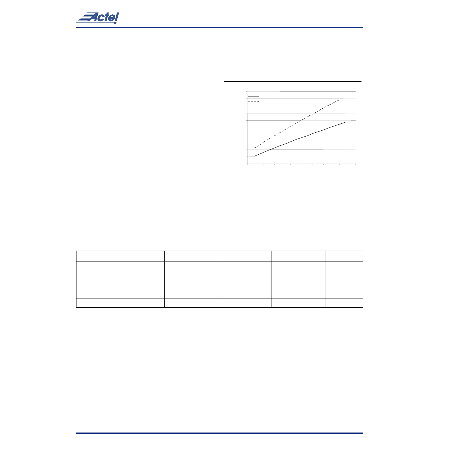
Figure 16 • Power Consumption of a 500K Device
100 120
Operating Conditions
Absolute Maximum Ratings
Parameter Condition Minimum Maximum Units
Supply Voltage Core (V
Supply Voltage IO Ring (V
DC Input Voltage –0.3 V
PCI DC Input Voltage –0.5 V
DC Input Clamp Current (IIK) V
Note: Stresses beyond those listed under Absolute Maximum ratings can cause permanent damage to the device. Exposure to maximum rated
conditions for extended periods can adversely affect device reliability. Operation of the device at these conditions or any others beyond
those listed in the Recommended Operating Conditions table on page 15 is not implied.
) –0.3 3.0 V
DDL
) –0.3 4.0 V
DDP
+ 0.3 V
DDP
+ 0.5 V
DDP
< 0 or > V
IN
DDP
–10 +10 mA
14
Page 15
Temperature Maximums
ProASIC™ 500K Family
Parameter Min. Max. Units
Retention
Storage Temperature –65 +150 °C N/A
Storage Temperature—Programmed –65 +110 °C 20 years
Program
Programming Limits and Recommended Operating Conditions
Junction T emperature
Product Grade
Programming
Cycles
Program
Retention
Min. Max.
Commercial 500 20 years 0°C 110°C
Industrial 500 20 years –40°C 110°C
Supply Voltages
Mode V
DDL
V
DDP
V
PP
V
PN
Single V oltage 2.5V 2.5V 2.5V ≤ VPP ≤ 16.5 V –12V ≤ VPN ≤ 0V
Mixed V oltage 2.5V 3.3V 3.3V ≤ V
Recommended Operating Conditions
≤ 16.5V –12V ≤ VPN ≤ 0V
PP
Parameter Symbol Limits
Commercial
DC Supply Voltage (2.5V I/Os) V
DC Supply Voltage (3.3V, 2.5V I/Os) V
Operation Ambient Temperature Range T
Operation Junction Temperature (maximum) T
DDL
V
& V
DDP
DDL
A
J
DDP
2.3V to 2.7V
3.0V to 3.6V
2.3V to 2.7V
0°C to 70°C
≤ 110°C
Industrial
DC Supply Voltage (2.5V I/Os) V
DDL
DC Supply Voltage (2.5V, 3.3V I/Os) V
V
Operation Ambient Temperature Range T
Operation Junction Temperature (maximum) T
& V
DDP
DDL
A
J
DDP
2.3V to 2.7V
3.0V to 3.6V
2.3V to 2.7V
–40°C to 85°C
≤ 110°C
15
Page 16
DC Electrical Specifications (V
DDP
= 2.5V)
Symbol Parameter Conditions Min. Typ. Max. Units
V
V
V
V
V
I
IN
I
DDQ
I
OZ
I
OSH
I
OSL
C
C
DDP
OH
OL
IH
IL
I/O
CLK
, V
DDL
Supply V oltage 2.3 2.7 V
Output High Voltage
High Drive
Low Drive
= –2.0 mA
I
OH
I
= –4.0 mA
OH
I
= –8.0 mA
OH
= –1.0 mA
I
OH
I
= –2.0 mA
OH
I
= –4.0 mA
OH
2.1
2.0
1.7
2.1
2.0
1.7
V
Output Low Voltage
High Drive
Low Drive
Input High Voltage 1.7 V
= 5.0 mA
I
OL
I
= 10.0 mA
OL
I
= 15.0 mA
OL
= 2.0 mA
I
OL
I
= 3.5 mA
OL
I
= 5.0 mA
OL
0.2
0.4
0.7
0.2
0.4
0.7
+ 0.3 V
DDP
V
Input Low Voltage –0.3 .7 V
Input Current
Input Current
Quiescent Supply Current VIN = V
3-State Output Leakage Current VOH = VSS or V
with pull-up
without pull-up
†
or V
SS
DDL
DDL
–20
–10
–100
10
µA
µA
1.0 10 mA
–10 +10 µA
Output Short Circuit Current High
High Drive
Low Drive
–120
–100
mA
Output Short Circuit Current Low
High Drive
Low Drive
100
30
mA
I/O Pad Capacitance 8pF
Clock Input Pad Capacitance 8 pF
Notes: All process conditions. Junction Temperature: –40 to +110°C.
† No pull-up resistor.
16
Page 17
ProASIC™ 500K Family
DC Electrical Specifications (V
= 3.3V)
DDP
Symbol Parameter Conditions Min. Typ. Max. Units
V
DDP
V
DDL
V
OH
V
OL
V
IH
V
IL
I
IN
I
DDQ
Supply V oltage 3.0 3.6 V
Supply Voltage, Logic Array 2.3 2.7 V
Output High Voltage
3.3V I/O, High Drive
3.3V I/O, Low Drive
2.5V I/O, High Drive
2.5V I/O, Low Drive
= –3.0 mA
I
OH
I
= –5.0 mA
OH
I
= –10.0 mA
OH
= –2.0 mA
I
OH
I
= –3.0 mA
OH
I
= –6.0 mA
OH
= –0.5 mA
I
OH
I
= –1.0 mA
OH
I
= –2.0 mA
OH
= –0.5 mA
I
OH
I
= –1.0 mA
OH
I
= –2.0 mA
OH
V
DDP
0.9
V
DDP
0.9
– 0.2
* VDDP
2.4
– 0.2
* VDDP
2.4
2.1
2.0
1.7
2.1
2.0
1.7
Output Low Voltage
3.3V I/O, High Drive
3.3V I/O, Low Drive
2.5V I/O, High Drive
2.5V I/O, Low Drive
= 7.5 mA
I
OL
I
= 12.0 mA
OL
I
= 15.0 mA
OL
= 2.5 mA
I
OL
I
= 4.0 mA
OL
I
= 5.0 mA
OL
= 7.5 mA
I
OL
I
= 15.0 mA
OL
I
= 24.0 mA
OL
= 2.5 mA
I
OL
I
= 5.0 mA
OL
I
= 8.0 mA
OL
0.1
0.1
0.2
* VDDP
0.4
0.2
* VDDP
0.4
0.2
0.4
0.7
0.2
0.4
0.7
Input High Voltage
LVTTL/LVCMOS
2.5V Mode
2
1.7
V
V
DDP
DDP
+ 0.3
+ 0.3
Input Low Voltage
LVTTL/LVCMOS
2.5V Mode
–0.3
–0.3
0.8
0.7
Input Current
LVTTL/LVCMOS
LVTTL/LVCMOS
Quiescent Supply Current VIN = V
with pull-up
without pull-up
†
or V
SS
DD
–40
–10
–200
10
µA
µA
1.0 10 mA
V
V
V
V
V
V
Notes: Refer to PCI Specifications Revision 2.2. for 3.3V high drive, high slew-rate output pads, and all 3.3V input/clock pads.
† No pull-up resistor.
17
Page 18
DC Electrical Specifications (V
= 3.3V) (Continued)
DDP
Symbol Parameter Conditions Min. Typ. Max. Units
I
OZ
I
OSH
I
OSL
C
C
I/O
CLK
3-State Output Leakage Current VOH = V
Output Short Circuit Current High
3.3V I/O, High Drive
3.3V I/O, Low Drive
2.5V I/O, High Drive
2.5V I/O, Low Drive
Output Short Circuit Current Low
3.3V I/O, High Drive
3.3V I/O, Low Drive
2.5V I/O, High Drive
2.5V I/O, Low Drive
I/O Pad Capacitance 8pF
Clock Input Pad Capacitance 8 pF
SS
†
or V
DD
–10 +10 µA
–200
mA
–140
–100
–100
160
mA
50
160
50
Notes: Refer to PCI Specifications Revision 2.2. for 3.3V high drive, high slew-rate output pads, and all 3.3V input/clock pads.
† No pull-up resistor.
18
Page 19

Timing Characteristics
ProASIC™ 500K Family
EN
A
PAD
OTBx
A
PAD
V
OL
50%
t
DLH
50%
V
OH
50%
t
DHL
50%
EN
PAD
50%
V
CC
t
ENZL
50%
50%
V
OL
10%
EN
PAD
GND
50%
t
ENZH
50%
V
OH
50%
90%
Figure 17 • Tri-State Buffer Delays
Table 3 • Tri-State Buffer Delays
(Worst-Case Commercial Conditions, V
DDP
= 3.0V, V
Macro T ype Description
OTB33PH 3.3V, PCI Output Current, High Slew Rate 4.41 4.28 4.40 3.71 ns
OTB33PN 3.3V, PCI Output Current, Nominal Slew Rate 4.91 6.08 4.90 5.46 ns
OTB33PL 3.3V, PCI Output Current, Low Slew Rate 5.51 7.41 5.50 6.86 ns
OTB33LH 3.3V, Low Output Current, High Slew Rate 6.23 6.90 6.24 6.09 ns
OTB33LN 3.3V, Low Output Current, Nominal Slew Rate 6.98 9.63 6.98 9.26 ns
OTB33LL 3.3V, Low Output Current, Low Slew Rate 7.80 12.56 7.80 12.28 ns
OTB25HH 2.5V, High Output Current, High Slew Rate 7.15 3.73 7.15 3.48 ns
OTB25HN 2.5V, High Output Current, Nominal Slew Rate 7.54 5.41 7.54 5.14 ns
OTB25HL 2.5V, High Output Current, Low Slew Rate 8.45 6.66 8.45 6.38 ns
OTB25LH 2.5V, Low Output Current, High Slew Rate 10.77 5.74 10.76 5.37 ns
OTB25LN 2.5V, Low Output Current, Nominal Slew Rate 11.54 8.60 11.52 8.35 ns
OTB25LL 2.5V, Low Output Current, Low Slew Rate 12.39 11.37 12.38 11.12 ns
OTB25LPHH 2.5V, Low Power, High Output Current, High Slew Rate 5.30 5.29 5.27 4.57 ns
OTB25LPHN 2.5V, Low Power, High Output Current, Nominal Slew Rate 6.27 7.99 6.24 7.46 ns
OTB25LPHL 2.5V, Low Power, High Output Current, Low Slew Rate 7.15 10.20 7.12 9.74 ns
OTB25LPLH 2.5V, Low Power, Low Output Current, High Slew Rate 7.74 9.02 7.71 8.10 ns
OTB25LPLN 2.5V, Low Power, Low Output Current, Nominal Slew Rate 8.96 13.11 8.93 12.76 ns
OTB25LPLL 2.5V, Low Power, Low Output Current, Low Slew Rate 10.24 17.72 10.21 17.38 ns
Notes:
1. t
2. t
3. t
4. t
= Data-to-Pad HIGH
DLH
= Data-to-Pad LOW
DHL
= Enable-to-Pad, Z to HIGH
ENZH
= Enable-to-Pad, Z to LOW
ENZL
= 2.3V, 35 pF load, TJ = 70°C)
DDL
Max
t
DLH
Max
t
DHL
Max
t
ENZH
Max
t
ENZL
Units
19
Page 20

A
A
PAD
PAD
V
OBx
50%
OL
t
DLH
50%
V
OH
50%
t
DHL
50%
Figure 18 • Output Buffer Delays
Table 4 • Output Buffer Delays
(Worst-Case Commercial Conditions, V
DDP
= 3.0V, V
Macro T ype Description Max. t
OB33PH 3.3V, PCI Output Current, High Slew Rate 4.41 4.28 ns
OB33PN 3.3V, PCI Output Current, Nominal Slew Rate 4.91 6.08 ns
OB33PL 3.3V, PCI Output Current, Low Slew Rate 5.51 7.41 ns
OB33LH 3.3V, Low Output Current, High Slew Rate 6.23 6.90 ns
OB33LN 3.3V, Low Output Current, Nominal Slew Rate 6.98 9.63 ns
OB33LL 3.3V, Low Output Current, Low Slew Rate 7.80 12.56 ns
OB25HH 2.5V, High Output Current, High Slew Rate 7.15 3.73 ns
OB25HN 2.5V, High Output Current, Nominal Slew Rate 7.54 5.41 ns
OB25HL 2.5V, High Output Current, Low Slew Rate 8.45 6.66 ns
OB25LH 2.5V, Low Output Current, High Slew Rate 10.77 5.74 ns
OB25LN 2.5V, Low Output Current, Nominal Slew Rate 11.54 8.60 ns
OB25LL 2.5V, Low Output Current, Low Slew Rate 12.39 11.37 ns
OB25LPHH 2.5V, Low Power, High Output Current, High Slew Rate 5.30 5.29 ns
OB25LPHN 2.5V, Low Power, High Output Current, Nominal Slew Rate 6.27 7.99 ns
OB25LPHL 2.5V, Low Power, High Output Current, Low Slew Rate 7.15 10.20 ns
OB25LPLH 2.5V, Low Power, Low Output Current, High Slew Rate 7.74 9.02 ns
OB25LPLN 2.5V, Low Power, Low Output Current, Nominal Slew Rate 8.96 13.11 ns
OB25LPLL 2.5V, Low Power, Low Output Current, Low Slew Rate 10.24 17.72 ns
Notes:
1. t
2. t
= Data-to-Pad HIGH
DLH
= Data-to-Pad LOW
DHL
= 2.3V, 35 pF load, TJ = 70°C)
DDL
DLH
Max. t
DHL
Units
20
Page 21

PAD
IBx
ProASIC™ 500K Family
V
CC
PAD
Y
Y
50%
50%
V
CC
50%
0V
50%
GND
t
INYH
t
INYL
Figure 19 • Input Buffer Delays
Table 5 • Input Buffer Delays
(Worst-Case Commercial Conditions, V
DDP
= 3.0V, V
Macro T ype Description
IB25 2.5V, CMOS Input Levels, No Pull-up Resistor 2.26 0.70 ns
IB25LP 2.5V, CMOS Input Levels, Low Power 2.25 1.51 ns
IB33 3.3V, CMOS Input Levels, No Pull-up Resistor 1.98 1.02 ns
Notes:
1. t
2. t
= Input Pad-to-Y HIGH
INYH
= Input Pad-to-Y LOW
INYL
= 2.3V, TJ = 70°C)
DDL
Max.
t
INYH
Max.
t
INYL
Units
Table 6 • Global Input Buffer Delays
(Worst-Case Commercial Conditions, V
Macro T ype Description
GL25 2.5V, CMOS Input Levels 2.17 1.74 ns
GL25LP 2.5V, CMOS Input Levels 2.38 2.37 ns
GL33 3.3V, CMOS Input Levels 3.97 1.17 ns
GL25U 2.5V, CMOS Input Levels, with Pull-up Resistor 2.17 1.74 ns
GL25LPU 2.5V, CMOS Input Levels, Low Power, with Pull-up Resistor 2.38 2.37 ns
GL33U 3.3V, CMOS Input Levels, with Pull-up Resistor 3.97 1.17 ns
DDP
= 3.0V, V
= 2.3V, TJ = 70°C)
DDL
Max.
t
INYH
Max.
t
INYL
Units
Table 7 • Predicted Global Routing Delay*
(Worst-Case Commercial Conditions, V
Parameter Description Max. Units
t
RCKH
t
RCKL
t
RCKH
t
RCKL
* The timing delay difference between tile locations is less than 15ps.
Input Low to High (fully loaded row—32 inputs) 1.19 ns
Input High to Low (fully loaded row—32 inputs) 1.1 ns
Input Low to High (minimally loaded row—1 input) 0.89 ns
Input High to Low (minimally loaded row—1 input) 0.85 ns
DDP
= 3.0V, V
= 2.3V, TJ = 70°C)
DDL
Table 8 • Global Routing Skew
(Worst-Case Commercial Conditions, V
Parameter Description Max. Units
t
RCKSWH
t
RCKSHH
Maximum Skew Low to High 0.30 ns
Maximum Skew High to Low 0.26 ns
DDP
= 3.0V, V
= 2.3V, TJ = 70°C)
DDL
21
Page 22

A
B
Y
C
A
B
C
50%Y50%
50%
t
DALH
t
DAHL
50% 50%
t
DBLH
50%
t
DBHL
50% 50%
50%50%
t
DCLH
50%
t
DCHL
50%
Figure 20 • Module Delays
Table 9 • Sample Macrocell Library Listing
(Worst-Case Commercial Conditions, V
Cell Name Description
NAND2 2-Input NAND 0.42 ns
AND2 2-Input AND 0.40 ns
NOR3 3-Input NOR 0.42 ns
MUX2L 2-1 Mux with Active Low Select 0.42 ns
OA21 2-Input OR into a 2-Input AND 0.40 ns
XOR2 2-Input Exclusive OR 0.34 ns
LDL Active Low Latch (LH/HL) D: 0.26/0.21 t
DFFL Negative Edge-Triggered D-type Flip-Flop (LH/HL) CLK-Q:
Note: Assumes fanout of two.
= 2.3V, TJ = 70º C)
DDL
Maximum
Intrinsic Delay
0.42/0.37
Minimum
Setup/Hold Units
0.54
setup
t
0.20
hold
0.43
t
setup
t
0.20
hold
ns
ns
22
Page 23

Embedded Memory Specifications
This section focuses on the embedded memory of the
ProASIC 500K family. It describes the SRAM and FIFO
interface signals and includes timing diagrams that show the
relationships of signals as they pertain to single embedded
memory blocks (Table 10). Refer to Table 2 on page 9 for
basic RAM configurations.
Enclosed Timing Diagrams—SRAM Mode:
• Asynchronous RAM Read, Address Controlled, RDB=0
• Asynchronous RAM Read, RDB Controlled
• Asynchronous RAM Write
• Synchronous RAM Read, Access Timed Output Strobe
(Synchronous Transparent)
• Synchronous RAM Read, Pipeline Mode Outputs
(Synchronous Pipelined)
• Synchronous RAM Write
• Synchronous Write & Read to the Same Location
• Asynchronous Write & Synchronous Read to the Same
Location
• Asynchronous Write & Read to the Same Location
• Synchronous Write & Asynchronous Read to the Same
Location
ProASIC™ 500K Family
Note: The difference between synchronous transparent
and pipeline modes is the timing of all the output
signals from the memory. In transparent mode
the outputs will change within the same clock
cycle to reflect the data requested by the currently
valid access to the memory. However, if clock
cycles are short (high clock speed) the data
requires most of the clock cycle to change to valid
values (stable signals). This makes processing of
this data in the same clock cycle nearly
impossible. Most designers solve this problem by
adding registers at all outputs of the memory to
push the data processing into the next clock cycle.
In this setup, the whole cycle time can be used to
process the data. To simplify the use of this kind
of memory setup these registers have been
implemented as part of the memory primitive
and are available to the user in the synchronous
pipeline mode. In this mode the output signals
will change shortly after the second rising edge
following the initiation of the read access.
Table 10 • Memory Block SRAM Interface Signals
SRAM Signal Bits In/Out Description
WCLKS 1 IN Write clock used on synchronization on write side
RCLKS 1 IN Read clock used on synchronization on read side
RADDR<0:7> 8 IN Read address
RBLKB 1 IN Negative true read block select
RDB 1 IN Negative true read pulse
WADDR<0:7> 8 IN Write address
WBLKB 1 IN Negative true write block select
DI<0:8> 9 IN Input data bits <0:8>, <8> will be generated if PARGEN is true
WRB 1 IN Negative true write pulse
DO<0:8> 9 OUT Output data bits <0:8>
RPE 1 OUT Read parity error
WPE 1 OUT Write parity error
PARODD 1 IN Selects odd parity generation/detect when high, even when low
Notes: Not all signals shown are used in all modes.
23
Page 24

Synchronous RAM Read, Access Timed Output Strobe (Synchronous Transparent)
RCLK
RB=(RBD+RBLKB)
RADDR
RDATA
RPE
t
RACS
t
RDCS
Old Data Out
t
RDCH
t
RACH
New Valid
Address
t
OCH
t
RPCH
Cycle Start
t
CMH
t
OCA
t
RPC
t
CCYC
New Valid Data Out
t
CM
T
= 0°C to 110°C; V
J
Symbol t
Description Min. Max. Units Notes
xxx
= 2.3V to 2.7V
DDL
CCYC Cycle time 7.5 ns
CMH Clock high phase 3.0 ns
CML Clock low phase 3.0 ns
OCA New RDATA access from RCLK ↑ 7.5 ns
OCH Old RDATA valid from RCLK ↑ 3.0 ns
RACH RADDR hold from RCLK ↑ 0.5 ns
RACS RADDR setup to RCLK ↑ 1.0 ns
RDCH RDB hold from RCLK ↑ 0.5 ns
RDCS RDB setup to RCLK ↑ 1.0 ns
RPCA New RPE access from RCLK ↑ 9.5 ns
RPCH Old RPE valid from RCLK ↑ 3.0 ns
24
Page 25

Synchronous RAM Read, Pipeline Mode Outputs (Synchronous Pipelined)
ProASIC™ 500K Family
RCLK
RB=(RDB+RBLKB)
RADDR
RDATA
RPE
t
RACS
t
RACH
t
RDCH
t
RDCS
New Valid
Address
Cycle Start
t
CMH
Old Data Out
New Valid Data Out
Old RPE Out New RPE Out
t
t
t
OCH
t
RPCA
t
CML
t
CCYC
OCA
RPCH
T
= 0°C to 110°C; V
J
Symbol t
CCYC Cycle time 7.5 ns
CMH Clock high phase 3.0 ns
CML Clock low phase 3.0 ns
OCA New RDATA access from RCLK ↑ 2.0 ns
OCH Old RDATA valid from RCLK ↑ .75 ns
RACH RADDR hold from RCLK ↑ 0.5 ns
RACS RADDR setup to RCLK ↑ 1.0 ns
RDCH RDB hold from RCLK ↑ 0.5 ns
RDCS RDB setup to RCLK ↑ 1.0 ns
RPCA New RPE access from RCLK ↑ 4.0 ns
RPCH Old RPE valid from RCLK ↑ 1.0 ns
Description Min. Max. Units Notes
xxx
= 2.3V to 2.7V
DDL
25
Page 26

Asynchronous RAM Write
WB=(WRB+WBLKB)
WADDR
WDATA
WPE
= 0°C to 110°C; V
T
J
Symbol t
Description Min. Max. Units Notes
xxx
t
AWRS
t
WPDA
= 2.3V to 2.7V
DDL
t
t
WRML
DWRS
t
WRCYC
t
WRMH
t
AWRH
t
DWRH
t
WPDH
AWRH WADDR hold from WB ↑ 1.0 ns
AWRS WADDR setup to WB ↓ 0.5 ns
DWRH WDATA hold from WB ↑ 1.5 ns
DWRS WDATA setup to WB ↑ 0.5 ns PARGEN is inactive
DWRS WDATA setup to WB ↑ 2.5 ns PARGEN is active
WPDA WPE access from WDATA 3.0 ns WPE is invalid while
WPDH WPE hold from WDATA 1.0 ns PARGEN is active
WRCYC Cycle time 7.5 ns
WRMH WB high phase 3.0 ns Inactive
WRML WB low phase 3.0 ns Active
26
Page 27

Asynchronous RAM Read, Address Controlled, RDB=0
RADDR
RDATA
RPE
t
OAH
t
RPAH
t
OAA
t
RPAA
t
ACYC
ProASIC™ 500K Family
= 0°C to 110°C; V
T
J
Symbol t
Description Min. Max. Units Notes
xxx
= 2.3V to 2.7V
DDL
ACYC Read cycle time 7.5 ns
OAA New RDATA access from RADDR stable 7.5 ns
OAH Old RDATA hold from RADDR stable 3.0 ns
RPAA New RPE access from RADDR stable 10.0 ns
RPAH Old RPE hold from RADDR stable 3.0 ns
27
Page 28

Asynchronous RAM Read, RDB Controlled
RB=(RDB+RBLKB)
RDATA
RPE
t
ORDH
t
RPRDH
t
ORDA
t
RPRDA
t
RDML
t
RDCYC
t
RDMH
= 0°C to 110°C; V
T
J
Symbol t
Description Min. Max. Units Notes
xxx
= 2.3V to 2.7V
DDL
ORDA New RDATA access from RB ↓ 7.5 ns
ORDH Old RDATA valid from RB ↓ 3.0 ns
RDCYC Read cycle time 7.5 ns
RDMH RB high phase 3.0 ns Inactive setup to new cycle
RDML RB low phase 3.0 ns Active
RPRDA New RPE access from RB ↓ 9.5 ns
RPRDH Old RPE valid from RB ↓ 3.0 ns
28
Page 29

Synchronous RAM Write
ProASIC™ 500K Family
WCLK
WRB, WBLKB
WADDR, WDATA
WPE
t
WRCH, tWBCH
t
WRCS, tWBCS
t
DCS, tWDCS
t
DCH, tWACH
t
WPCH
Cycle Start
t
WPCA
t
CMH
t
CCYC
t
CML
T
= 0°C to 110°C; V
J
Symbol t
Description Min. Max. Units Notes
xxx
= 2.3V to 2.7V
DDL
CCYC Cycle time 7.5 ns
CMH Clock high phase 3.0 ns
CML Clock low phase 3.0 ns
DCH WDATA hold from WCLK ↑ 0.5 ns
DCS WDATA setup to WCLK ↑ 1.0 ns
WACH WADDR hold from WCLK ↑ 0.5 ns
WACS WADDR setup to WCLK ↑ 1.0 ns
WPCA New WPE access from WCLK ↑ 3.0 ns WPE is invalid while
WPCH Old WPE valid from WCLK ↑ 0.5 ns
WRCH,
WRB & WBLKB hold from WCLK ↑ 0.5 ns
PARGEN is active
WBCH
WRCS,
WRB & WBLKB setup to WCLK ↑ 1.0 ns
WBCS
Note: On simultaneous read and write accesses to the same location WDATA is output to RDATA.
29
Page 30

Synchronous Write & Read to the Same Location
RCLK
RDATA
Last Cycle Data
New Data*
WCLK
t
WCLKRCLKH
t
WCLKRCLKS
t
OCH
t
OCA
* New data is read if WCLK ↑ occurs before setup time.
The data stored is read if WCLK ↑ occurs after hold time.
= 0°C to 110°C; V
T
J
Symbol t
xxx
Description Min. Max. Units Notes
= 2.3V to 2.7V
DDL
CCYC Cycle time 7.5 ns
CMH Clock high phase 3.0 ns
CML Clock low phase 3.0 ns
WCLKRCLKS WCLK ↑ to RCLK ↑ setup time – 0.1 ns
WCLKRCLKH WCLK ↑ to RCLK ↑ hold time 7.0 ns
OCH Old RDATA valid from RCLK ↑ 3.0 ns
OCA New RDATA valid from RCLK ↑ 7.5 ns
OCA/OCH displayed for
Access Timed Output
Notes:
1. This behavior is valid for Access Timed Output and Pipelined Mode Output. Shown are the timings of an access timed output.
2. During synchronous write and synchronous read access to the same location, the new write data will be read out if the active write clock
edge occurs before or at the same time as the active read clock edge. The negative setup time insures this behavior for WCLK and RCLK
driven by the same design signal.
3. If WCLK changes after the hold time, the data will be read.
4. A setup or hold time violation will result in unknown output data.
30
Page 31

Asynchronous Write & Synchronous Read to the Same Location
RCLK
ProASIC™ 500K Family
RDATA
Last Cycle Data
New Data*
WB = {WRB + WBLKB}
WDATA
t
WCLKRCLKS
t
WCLKRCLKH
t
OCH
t
OCA
t
DWRRCLKS
t
DWRH
* New data is read if WB ↓ occurs before setup time.
The stored data is read if WB ↓ occurs after hold time.
= 0°C to 110°C; V
T
J
Symbol t
xxx
Description Min. Max. Units Notes
= 2.3V to 2.7V
DDL
CCYC Cycle time 7.5 ns
CMH Clock high phase 3.0 ns
CML Clock low phase 3.0 ns
WBRCLKS WB ↓ to RCLK ↑ setup time –0.1 ns
WBRCLKH WB ↓ to RCLK ↑ hold time 7.0 ns
OCH Old RDATA valid from RCLK ↑ 3.0 ns
OCA New RDATA valid from RCLK ↑ 7.5 ns
OCA/OCH displayed for
Access Timed Output
DWRRCLKS WDATA to RCLK ↑ setup time 0 ns
DWRH WDATA to WB ↑ hold time 1.5 ns
Notes:
1. This behavior is valid for Access Timed Output and Pipelined Mode Output. Shown are the timings of an access timed output.
2. In asynchronous write and synchronous read access to the same location, the new write data will be read out if the active write signal edge
occurs before or at the same time as the active read clock edge. If WB changes to low after hold time, the data will be read.
3. A setup or hold time violation will result in unknown output data.
31
Page 32

Asynchronous Write & Read to the Same Location
RB, RADDR
RDATA
OLD
NEWERNEW
WB = {WRB+WBLKB}
0°C to 110°C; V
T
J =
Symbol t
xxx
t
ORDA
t
ORDH
t
RAWRS
= 2.3V to 2.7V
DDL
t
OWRA
t
OWRH
Description Min. Max. Units Notes
t
RAWRH
ORDA New RDATA access from RB ↓ 7.5 ns
ORDH Old RDATA valid from RB ↓ 3.0 ns
OWRA New RDATA access from WB ↑ 3.0 ns
OWRH Old RDATA valid from WB ↑ 0.5 ns
RAWRS RB ↓ or RADDR from WB ↓ 5.0 ns
RAWRH RB ↑ or RADDR from WB ↑ 5.0 ns
Notes:
1. During an asynchronous read cycle, each write operation (sync. or async.) to the same location will automatically trigger a read
operation which updates the read data.
2. Violation or RAWRS will disturb access to the OLD data.
3. Violation of RAWRH will disturb access to the NEWER data.
32
Page 33

Synchronous Write & Asynchronous Read to the Same Location
RB, RADDR
ProASIC™ 500K Family
RDATA
OLD
NEW NEWER
WCLK
t
RAWCLKS
T
= 0°C to 110°C; V
J
Symbol t
xxx
t
ORDA
t
ORDH
t
OWRA
t
OWRH
= 2.3V to 2.7V
DDL
Description Min. Max. Units Notes
t
RAWCLKH
ORDA New RDATA access from RB ↓ 7.5 ns
ORDH Old RDATA valid from RB ↓ 3.0 ns
OWRA New RDATA access from WCLK ↓ 3.0 ns
OWRH Old RDATA valid from WCLK ↓ 0.5 ns
RAWCLKS RB ↓ or RADDR from WCLK ↑ 5.0 ns
RAWCLKH RB ↑ or RADDR from WCLK ↓ 5.0 ns
Notes:
1. During an asynchronous read cycle, each write operation (sync. or async.) to the same location will automatically trigger a read
operation which updates the read data.
2. Violation of RAWCLKS will disturb access to OLD data.
3. Violation of RAWCLKH will disturb access to NEWER data.
33
Page 34

Asynchronous FIFO Full and Empty Transitions
The asynchronous FIFO accepts writes and reads while not
full or not empty, respectively. When the FIFO is full, all
writes are inhibited. Conversely, when the FIFO is empty, all
reads are inhibited. A problem is created if the FIFO is
written during the transition out of full to not full or read
during the transition out of empty to not empty. The exact
time at which the write (read) operation changes from
inhibited to accepted after the read (write) signal which
causes the transition from full (empty) to not full (empty) is
indeterminate. This indeterminate period starts 1 ns after the
RB (WB) transition which deactivates full (not empty) and
ends 3 ns after the RB (WB) transition, for slow cycles. For
fast cycles, the indeterminate period ends 3 ns (7.5 ns – RDL
(WRL)) after the RB (WB) transition, whichever is later.
The timing diagram for write is shown in Figure 21 on page
35. The timing diagram for read is shown in Figure 22 on page
35. For basic RAM configurations, see Table 2 on page 9.
Enclosed Timing Diagrams—FIFO Mode:
• Asynchronous FIFO Read
• Asynchronous FIFO Write
• Synchronous FIFO Read, Access Timed Output
Strobe (Synchronous Transparent)
• Synchronous FIFO Read, Pipeline Mode Outputs
(Synchronous Pipelined)
• Synchronous FIFO Write
• FIFO Reset
Table 11 • Memory Block FIFO Interface Signals
FIFO Signal Bits In/Out Description
WCLK 1 IN Write clock used on synchronization on write side
RCLK 1 IN Read clock used on synchronization on read side
LEVEL <0:7> 8 IN Direct configuration implements static flag logic.
RBLKB 1 IN Negative true read block select.
RDB 1 IN Negative true read pulse.
RESET 1 IN Negative true reset for FIFO pointers.
WBLKB 1 IN Negative true write block select.
DI<0:8> 9 IN Input data bits <0:8>, <8> will be generated if PARGEN is true.
WRB 1 IN Negative true write pulse.
FULL, EMPTY 2 OUT FIFO flags. FULL prevents write and EMPTY prevents read.
EQTH, GEQTH 2 OUT
DO<0:8> 9 OUT Output data bits <0:8>
RPE 1 OUT Read parity error.
WPE 1 OUT Write parity error.
LGDEP <0:2> 3 IN Configures DEPTH of the FIFO to 2
PARODD 1 IN Selects odd parity generation/detect when high, even when low.
EQTH is true when the FIFO holds (LEVEL) words. GEQTH is true when the
FIFO holds (LEVEL) words or more.
(LGDEP+1)
34
Page 35

FULL
RB
ProASIC™ 500K Family
Write
cycle
WB
Figure 21 • Write Timing Diagram
EMPTY
WB
Read
cycle
Write acceptedWrite inhibited
1ns
3ns
Read acceptedRead inhibited
1ns
RB
Figure 22 • Read Timing Diagram
3ns
35
Page 36

Asynchronous FIFO Read
RB=(RDB+RBLKB)
RDATA
RPE
WB
EMPTY
FULL
EQTH, GETH
t
RDWRS
t
ORDH
t
RPRDH
Cycle Start
t
ORDA
t
RPRDA
t
RDL
t
RDCYC
t
THRDH
t
THRDA
t
RDH
(Empty inhibits read)
t
, t
ERDH
FRDH
t
, t
ERDA
FRDA
T
= 0°C to 110°C; V
J
Symbol t
ERDH,
FRDH,
Description Min. Max. Units Notes
xxx
Old EMPTY, FULL, EQTH, & GETH valid
hold time from RB ↑
THRDH
ERDA New EMPTY access from RB ↑ 3.0
FRDA FULL↓ access from RB ↑ 3.0
= 2.3V to 2.7V
DDL
0.5 ns Empty/full/thresh are invalid
from the end of hold until the
new access is complete
1
1
ns
ns
ORDA New RDATA access from RB ↓ 7.5 ns
ORDH Old RDATA valid from RB ↓ 3.0 ns
RDCYC Read cycle time 7.5 ns
RDWRS WB ↑, clearing EMPTY, setup to
RB ↓
3.0
2
ns Enabling the read operation
1.0 ns Inhibiting the read operation
RDH RB high phase 3.0 ns Inactive
RDL RB low phase 3.0 ns Active
RPRDA New RPE access from RB ↓ 9.5 ns
RPRDH Old RPE valid from RB ↓ 4.0 ns
THRDA EQTH or GETH access from RB↑ 4.5 ns
Notes:
1. At fast cycles, ERDA & FRDA = MAX (7.5 ns – RDL), 3.0 ns
2. At fast cycles, RDWRS (for enabling read) = MAX (7.5 ns – WRL), 3.0 ns
36
Page 37

Asynchronous FIFO Write
ProASIC™ 500K Family
WB=(WRB+WBLKB)
WDATA
WPE
RB
FULL
EMPTY
EQTH, GETH
t
WRRDS
t
WPDA
t
DWRS
t
EWRH
t
EWRA
Cycle Start
, t
FWRH
, t
FWRA
t
WRL
t
WRCYC
t
THWRH
t
THWRA
t
WRH
(Full inhibits write)
t
DWRH
t
WPDH
T
= 0°C to 110°C; V
J
Symbol t
Description Min. Max. Units Notes
xxx
= 2.3V to 2.7V
DDL
DWRH WDATA hold from WB ↑ 1.5 ns
DWRS WDATA setup to WB ↑ 0.5 ns PARGEN is inactive.
DWRS WDATA setup to WB ↑ 2.5 ns PARGEN is active.
EWRH,
FWRH,
THWRH
EWRA EMPTY ↓ access from WB ↑ 3.0
FWRA New FULL access from WB ↑ 3.0
Old EMPTY, FULL, EQTH, & GETH valid
hold time after WB ↑
0.5 ns Empty/full/thresh are invalid
from the end of hold until the
new access is complete.
1
1
ns
ns
THWRA EQTH or GETH access from WB ↑ 4.5 ns
WPDA WPE access from WDATA 3.0 ns
WPDH WPE hold from WDATA 1.0 ns
WPE is invalid while
PARGEN is active.
WRCYC Cycle time 7.5 ns
WRRDS RB ↑, clearing FULL, setup to
WB ↓
3.0
2
ns Enabling the write operation.
1.0 Inhibiting the write operation.
WRH WB high phase 3.0 ns Inactive
WRL WB low phase 3.0 ns Active
Notes:
1. At fast cycles, EWRA, FWRA = MAX (7.5 ns – WRL), 3.0 ns
2. At fast cycles, WRRDS (for enabling write) = MAX (7.5 ns – RDL), 3.0 ns
37
Page 38

Synchronous FIFO Read, Access Timed Output Strobe (Synchronous Transparent)
RCLK
RDB
RDATA
RPE
EMPTY
FULL
EQTH, GETH
Cycle Start
Old Data Out New Valid Data Out (Empty Inhibits Read)
t
RDCS
t
RDCH
t
OCH
t
RPCH
t
OCA
t
RPCA
t
CMH
t
CCYC
t
THCBH
t
THCB
t
CML
t
ECBH
t
ECBA
, t
, t
FCBH
FCBA
T
= 0°C to 110°C; V
J
Symbol t
Description Min. Max. Units Notes
xxx
= 2.3V to 2.7V
DDL
CCYC Cycle time 7.5 ns
CMH Clock high phase 3.0 ns
CML Clock low phase 3.0 ns
ECBA New EMPTY access from RCLK ↓ 3.0
FCBA FULL ↓ access from RCLK ↓ 3.0
ECBH,
FCBH,
Old EMPTY, FULL, EQTH, & GETH valid
hold time from RCLK ↓ 1.0 ns
1
1
THCBH
OCA New RDATA access from RCLK ↑ 7.5 ns
OCH Old RDATA valid from RCLK ↑ 3.0 ns
RDCH RDB hold from RCLK ↑ 0.5 ns
RDCS RDB setup to RCLK ↑ 1.0 ns
RPCA New RPE access from RCLK ↑ 9.5 ns
RPCH Old RPE valid from RCLK ↑ 3.0 ns
THCBA EQTH or GETH access from RCLK ↓ 4.5 ns
Note:
1. At fast cycles, ECBA & FCBA = MAX (7.5 .ns – CMH), 3.0 ns
ns
ns
Empty/full/thresh are invalid
from the end of hold until the
new access is complete
38
Page 39

Synchronous FIFO Read, Pipeline Mode Outputs (Synchronous Pipelined)
ProASIC™ 500K Family
RCLK
RDB
RDATA
RPE
EMPTY
FULL
EQTH, GETH
t
RDCS
t
RDCH
Cycle Start
t
ECBH
t
CMH
Old Data Out New Valid Data Out
Old RPE Out New RPE Out
, t
FCBH
t
THCBH
t
THCB
t
RPCA
t
CML
t
CCYC
t
OCA
t
ECBA
t
RPCH
t
OCH
, t
FCBA
T
= 0°C to 110°C; V
J
Symbol t
Description Min. Max. Units Notes
xxx
= 2.3V to 2.7V
DDL
CCYC Cycle time 7.5 ns
CMH Clock high phase 3.0 ns
CML Clock low phase 3.0 ns
ECBA New EMPTY access from RCLK ↓ 3.0
FCBA FULL ↓ access from RCLK ↓ 3.0
ECBH,
FCBH,
Old EMPTY, FULL, EQTH, & GETH valid
hold time from RCLK ↓
1
1
1.0 ns Empty/full/thresh are invalid
THCBH
OCA New RDATA access from RCLK ↑ 2.0 ns
OCH Old RDATA valid from RCLK ↑ 0.75 ns
RDCH RDB hold from RCLK ↑ 0.5 ns
RDCS RDB setup to RCLK ↑ 1.0 ns
RPCA New RPE access from RCLK ↑ 4.0 ns
RPCH Old RPE valid from RCLK ↑ 1.0 ns
THCBA EQTH or GETH access from RCLK ↓ 4.5 ns
Note:
1. At fast cycles, ECBA & FCBA = MAX (7.5 ns – CMS), 3.0 ns
ns
ns
from the end of hold until the
new access is complete
39
Page 40

Synchronous FIFO Write
WCLK
WRB, WBLKB
WDATA
WPE
FULL
EMPTY
EQTH, GETH
t
, t
WRCH
WBCH
t
, t
WRCS
WBCS
t
DCS
t
WPCH
t
DCS
Cycle Start
t
WPCA
t
CMH
t
CCYC
t
THCBH
t
CLM
(Full Inhibits Write)
t
, t
ECBH
FCBH
t
, t
ECBA
FCBA
t
, t
ECBH
FCBH
= 0°C to 110°C; V
T
J
Symbol t
xxx
= 2.3V to 2.7V
DDL
Description Min. Max. Units Notes
CCYC Cycle time 7.5 ns
CMH Clock high phase 3.0 ns
CML Clock low phase 3.0 ns
DCH WDATA hold from WCLK ↑ 0.5 ns
DCS WDATA setup to WCLK ↑ 1.0 ns
FCBA New FULL access from WCLK ↓ 3.0
ECBA EMPTY↓ access from WCLK ↓ 3.0
ECBH,
FCBH,
Old EMPTY, FULL, EQTH, & GETH valid
hold time from WCLK ↓
1
1
1.0 ns Empty/full/thresh are invalid
THCBH
THCBA EQTH or GETH access from WCLK ↓ 4.5 ns
WPCA New WPE access from WCLK ↑ 3.0 ns
WPCH Old WPE valid from WCLK ↑ 0.5 ns
WRCH,
WRB & WBLKB hold from WCLK ↑ 0.5 ns
WBCH
WRCS,
WRB & WBLKB setup to WCLK ↑ 1.0 ns
WBCS
Note:
1. At fast cycles, ECBA & FCBA = MAX (7.5 ns – CMH), 3.0 ns
ns
ns
from the end of hold until the
new access is complete
WPE is invalid while
PARGEN is active
40
Page 41

FIFO Reset
ProASIC™ 500K Family
RESETB
t
WBRSS
Cycle Start
Cycle Start
t
t
WBRSH
CBRSH
WB*
WCLK, RCLK
FULL
EMPTY
EQTH, GETH
t
, t
ERSA
FRSA
t
THRSA
t
CBRSS
t
RSL
*WB = WRB + WBLRB
= 0°C to 110°C; V
T
J
Symbol t
Description Min. Max. Units Notes
xxx
= 2.3V to 2.7V
DDL
CBRSH WCLK or RCLK ↑ hold from RESETB ↑ 1.5 ns Synchronous mode only
CBRSS WCLK or RCLK ↓ setup to RESETB ↑ 1.5 ns Synchronous mode only
ERSA New EMPTY ↑ access from RESETB ↓ 3.0 ns
FRSA FULL ↓ access from RESETB ↓ 3.0 ns
RSL RESETB low phase 7.5 ns
THRSA EQTH or GETH access from RESETB ↓ 4.5 ns
WBRSH WB ↓ hold from RESETB ↑ 1.5 ns Asynchronous mode only
WBRSS WB ↑ setup to RESETB ↑ 1.5 ns Asynchronous mode only
41
Page 42

Pin Description
I/O User Input/Output
The I/O pin functions as an input, output, three-state, or
bi-directional buffer. Input and output signal levels are
compatible with standard LVTTL and LVCMOS specifications.
Unused I/O pins are configured as inputs with pull-up resistor.
N/C No Connect
To maintain compatibility with future Actel ProASIC products
it is recommended that this pin not be connected to the
circuitry on the board.
GL Global Input Pin
Low skew input pin for clock or other global signals. Input
only. This pin can be configured with a pull-up resistor.
GND Ground
Common ground supply voltage.
V
DDL
Logic Array Power Supply Pin
2.5V supply voltage.
V
I/O Pad Power Supply Pin
DDP
2.5V or 3.3V supply voltage.
V
PP
This pin must be connected to V
Programming Supply Pin
during normal operation,
DDP
or it can remain at 16.5V in an ISP application. This pin must
not float.
V
PN
Programming Supply Pin
This pin must be connected to GND during normal operation,
or it can remain at –12V in an ISP application. This pin must
not float.
TMS Test Mode Select
The TMS pin controls the use of JTAG circuitry.
TCK Test Clock
Clock input pin for JTAG.
TDI Test Data In
Serial input for JTAG.
TDO Test Data Out
Serial output for JTAG.
TRST Test Reset Input
An optimal JTAG reset pin.
RCK Running Clock
A free running clock is needed during programming if the
programmer cannot guarantee that TCK will be
uninterrupted.
42
Page 43

Package Pin Assignments
208-Pin PQFP
208
1
ProASIC™ 500K Family
208-Pin PQFP
43
Page 44

208-Pin PQFP
Pin
Number
A500K050
Function
A500K130
Function
A500K180
Function
A500K270
Function
Pin
Number
A500K050
Function
1 GND GND GND GND 53 V
DDP
A500K130
Function
V
DDP
A500K180
Function
V
DDP
2 I/O I/O I/O I/O 54 I/O I/O I/O I/O
3 I/O I/O I/O I/O 55 I/O I/O I/O I/O
4 I/O I/O I/O I/O 56 I/O I/O I/O I/O
5 I/O I/O I/O I/O 57 I/O I/O I/O I/O
6 I/O I/O I/O I/O 58 I/O I/O I/O I/O
7 I/O I/O I/O I/O 59 I/O I/O I/O I/O
8 I/O I/O I/O I/O 60 I/O I/O I/O I/O
9 I/O I/O I/O I/O 61 I/O I/O I/O I/O
10 I/O I/O I/O I/O 62 I/O I/O I/O I/O
11 I/O I/O I/O I/O 63 I/O I/O I/O I/O
12 I/O I/O I/O I/O 64 I/O I/O I/O I/O
13 I/O I/O I/O I/O 65 GND GND GND GND
14 I/O I/O I/O I/O 66 I/O I/O I/O I/O
15 I/O I/O I/O I/O 67 I/O I/O I/O I/O
16 V
DDL
V
DDL
V
DDL
V
DDL
68 I/O I/O I/O I/O
17 GND GND GND GND 69 I/O I/O I/O I/O
18 I/O I/O I/O I/O 70 I/O I/O I/O I/O
19 I/O I/O I/O I/O 71 V
20 I/O I/O I/O I/O 72 V
DDL
DDP
V
V
DDL
DDP
V
DDL
V
DDP
21 I/O I/O I/O I/O 73 I/O I/O I/O I/O
22 V
DDP
V
DDP
V
DDP
V
DDP
74 I/O I/O I/O I/O
23 I/O I/O I/O I/O 75 I/O I/O I/O I/O
24 I/O I/O I/O I/O 76 I/O I/O I/O I/O
25 GL GL GL GL 77 I/O I/O I/O I/O
26 GL GL GL GL 78 I/O I/O I/O I/O
27 I/O I/O I/O I/O 79 I/O I/O I/O I/O
28 I/O I/O I/O I/O 80 I/O I/O I/O I/O
29 GND GND GND GND 81 GND GND GND GND
30 I/O I/O I/O I/O 82 I/O I/O I/O I/O
31 I/O I/O I/O I/O 83 I/O I/O I/O I/O
32 I/O I/O I/O I/O 84 I/O I/O I/O I/O
33 I/O I/O I/O I/O 85 I/O I/O I/O I/O
34 I/O I/O I/O I/O 86 I/O I/O I/O I/O
35 I/O I/O I/O I/O 87 I/O I/O I/O I/O
36 V
DDL
V
DDL
37 I/O I/O I/O I/O 89 V
V
DDL
V
DDL
88 V
DDL
DDP
V
V
DDL
DDP
V
DDL
V
DDP
38 I/O I/O I/O I/O 90 I/O I/O I/O I/O
39 I/O I/O I/O I/O 91 I/O I/O I/O I/O
40 V
DDP
V
DDP
V
DDP
V
DDP
92 I/O I/O I/O I/O
41 GND GND GND GND 93 I/O I/O I/O I/O
42 I/O I/O I/O I/O 94 I/O I/O I/O I/O
43 I/O I/O I/O I/O 95 I/O I/O I/O I/O
44 I/O I/O I/O I/O 96 I/O I/O I/O I/O
45 I/O I/O I/O I/O 97 GND GND GND GND
46 I/O I/O I/O I/O 98 I/O I/O I/O I/O
47 I/O I/O I/O I/O 99 I/O I/O I/O I/O
48 I/O I/O I/O I/O 100 I/O I/O I/O I/O
49 I/O I/O I/O I/O 101 TCK, I/O TCK, I/O TCK, I/O TCK, I/O
50 I/O I/O I/O I/O 102 TDI, I/O TDI, I/O TDI, I/O TDI, I/O
51 I/O I/O I/O I/O 103 TMS, I/O TMS, I/O TMS, I/O TMS, I/O
52 GND GND GND GND 104 V
DDP
V
DDP
V
DDP
A500K270
Function
V
DDP
V
DDL
V
DDP
V
DDL
V
DDP
V
DDP
44
Page 45

ProASIC™ 500K Family
208-Pin PQFP (Continued)
Pin
Number
105 GND GND GND GND 157 V
106 V
107 V
A500K050
Function
PP
PN
A500K130
Function
V
PP
V
PN
A500K180
Function
V
PP
V
PN
A500K270
Function
V
PP
V
PN
Pin
Number
A500K050
Function
DDP
A500K130
Function
V
DDP
A500K180
Function
V
DDP
158 I/O I/O I/O I/O
159 I/O I/O I/O I/O
108 TDO, I/O TDO, I/O TDO, I/O TDO, I/O 160 I/O I/O I/O I/O
109 TRST, I/O TRST, I/O TRST, I/O TRST, I/O 161 I/O I/O I/O I/O
110 RCK, I/O RCK, I/O RCK, I/O RCK, I/O 162 GND GND GND GND
111 I/O I/O I/O I/O 163 I/O I/O I/O I/O
112 I/O I/O I/O I/O 164 I/O I/O I/O I/O
113 I/O I/O I/O I/O 165 I/O I/O I/O I/O
114 I/O I/O I/O I/O 166 I/O I/O I/O I/O
115 I/O I/O I/O I/O 167 I/O I/O I/O I/O
116 I/O I/O I/O I/O 168 I/O I/O I/O I/O
117 I/O I/O I/O I/O 169 I/O I/O I/O I/O
118 I/O I/O I/O I/O 170 V
119 I/O I/O I/O I/O 171 V
DDP
DDL
V
V
DDP
DDL
V
V
DDP
DDL
120 I/O I/O I/O I/O 172 I/O I/O I/O I/O
121 I/O I/O I/O I/O 173 I/O I/O I/O I/O
122 GND GND GND GND 174 I/O I/O I/O I/O
123 V
DDP
V
DDP
V
DDP
V
DDP
175 I/O I/O I/O I/O
124 I/O I/O I/O I/O 176 I/O I/O I/O I/O
125 I/O I/O I/O I/O 177 I/O I/O I/O I/O
126 V
DDL
V
DDL
V
DDL
V
DDL
178 GND GND GND GND
127 I/O I/O I/O I/O 179 I/O I/O I/O I/O
128 I/O I/O I/O I/O 180 I/O I/O I/O I/O
129 I/O I/O I/O I/O 181 I/O I/O I/O I/O
130 GND GND GND GND 182 I/O I/O I/O I/O
131 I/O I/O I/O I/O 183 I/O I/O I/O I/O
132 I/O I/O I/O I/O 184 I/O I/O I/O I/O
133 GL GL GL GL 185 I/O I/O I/O I/O
134 GL GL GL GL 186 V
135 I/O I/O I/O I/O 187 V
DDP
DDL
V
V
DDP
DDL
V
V
DDP
DDL
136 I/O I/O I/O I/O 188 I/O I/O I/O I/O
137 I/O I/O I/O I/O 189 I/O I/O I/O I/O
138 V
DDP
V
DDP
V
DDP
V
DDP
190 I/O I/O I/O I/O
139 I/O I/O I/O I/O 191 I/O I/O I/O I/O
140 I/O I/O I/O I/O 192 I/O I/O I/O I/O
141 GND GND GND GND 193 I/O I/O I/O I/O
142 V
DDL
V
DDL
V
DDL
V
DDL
194 I/O I/O I/O I/O
143 I/O I/O I/O I/O 195 GND GND GND GND
144 I/O I/O I/O I/O 196 I/O I/O I/O I/O
145 I/O I/O I/O I/O 197 I/O I/O I/O I/O
146 I/O I/O I/O I/O 198 I/O I/O I/O I/O
147 I/O I/O I/O I/O 199 I/O I/O I/O I/O
148 I/O I/O I/O I/O 200 I/O I/O I/O I/O
149 I/O I/O I/O I/O 201 I/O I/O I/O I/O
150 I/O I/O I/O I/O 202 I/O I/O I/O I/O
151 I/O I/O I/O I/O 203 I/O I/O I/O I/O
152 I/O I/O I/O I/O 204 I/O I/O I/O I/O
153 I/O I/O I/O I/O 205 I/O I/O I/O I/O
154 I/O I/O I/O I/O 206 I/O I/O I/O I/O
155 I/O I/O I/O I/O 207 I/O I/O I/O I/O
156 GND GND GND GND 208 V
DDP
V
DDP
V
DDP
A500K270
Function
V
DDP
V
DDP
V
DDL
V
DDP
V
DDL
V
DDP
45
Page 46

Package Pin Assignments (Continued)
272-Pin PBGA (Bottom View)
A
B
C
D
E
F
G
H
J
K
L
M
N
P
R
T
U
V
W
Y
1234567891011121314151617181920
46
Page 47

ProASIC™ 500K Family
272-Pin PBGA
Pin
Number
A1 I/O I/O C7 I/O I/O F17 V
A500K050
Function
A500K130
Function
Pin
Number
A500K050
Function
A500K130
Function
Pin
Number
A500K050
Function
DDP
A2 I/O I/O C8 I/O I/O F18 I/O I/O
A3 I/O I/O C9 I/O I/O F19 I/O I/O
A4 I/O I/O C10 I/O I/O F20 I/O I/O
A5 I/O I/O C11 I/O I/O G1 I/O I/O
A6 I/O I/O C12 I/O I/O G2 I/O I/O
A7 I/O I/O C13 I/O I/O G3 I/O I/O
A8 I/O I/O C14 I/O I/O G4 I/O I/O
A9 I/O I/O C15 I/O I/O G17 I/O I/O
A10 I/O I/O C16 I/O I/O G18 I/O I/O
A11 I/O I/O C17 I/O I/O G19 I/O I/O
A12 I/O I/O C18 I/O I/O G20 I/O I/O
A13 I/O I/O C19 I/O I/O H1 I/O I/O
A14 I/O I/O C20 I/O I/O H2 I/O I/O
A15 I/O I/O D1 I/O I/O H3 I/O I/O
A16 I/O I/O D2 I/O I/O H4 I/O I/O
A17 I/O I/O D3 I/O I/O H17 I/O I/O
A18 I/O I/O D4 V
A19 I/O I/O D5 V
A20 I/O I/O D6 V
DDP
DDP
DDP
V
V
V
DDP
DDP
DDP
H18 I/O I/O
H19 I/O I/O
H20 GL GL
B1 I/O I/O D7 I/O I/O J1 I/O I/O
B2 I/O I/O D8 V
B3 I/O I/O D9 V
B4 I/O I/O D10 V
B5 I/O I/O D11 V
B6 I/O I/O D12 V
B7 I/O I/O D13 V
DDL
DDL
DDL
DDL
DDL
DDL
V
V
V
V
V
V
DDL
DDL
DDL
DDL
DDL
DDL
J2 GL GL
J3 GL GL
J4 V
DDL
J9 GND GND
J10 GND GND
J11 GND GND
B8 I/O I/O D14 I/O I/O J12 GND GND
B9 I/O I/O D15 V
B10 I/O I/O D16 V
B11 I/O I/O D17 V
DDP
DDP
DDP
V
V
V
DDP
DDP
DDP
J17 V
DDL
J18 GL GL
J19 I/O I/O
B12 I/O I/O D18 I/O I/O J20 I/O I/O
B13 I/O I/O D19 I/O I/O K1 I/O I/O
B14 I/O I/O D20 I/O I/O K2 I/O I/O
B15 I/O I/O E1 I/O I/O K3 I/O I/O
B16 I/O I/O E2 I/O I/O K4 V
DDL
B17 I/O I/O E3 I/O I/O K9 GND GND
B18 I/O I/O E4 V
B19 I/O I/O E17 V
DDP
DDP
V
V
DDP
DDP
K10 GND GND
K11 GND GND
B20 I/O I/O E18 I/O I/O K12 GND GND
C1 I/O I/O E19 I/O I/O K17 V
DDL
C2 I/O I/O E20 I/O I/O K18 I/O I/O
C3 I/O I/O F1 I/O I/O K19 I/O I/O
C4 I/O I/O F2 I/O I/O K20 I/O I/O
C5 I/O I/O F3 I/O I/O L1 I/O I/O
C6 I/O I/O F4 V
DDP
V
DDP
L2 I/O I/O
A500K130
Function
V
DDP
V
DDL
V
DDL
V
DDL
V
DDL
47
Page 48

272-Pin PBGA (Continued)
Pin
Number
A500K050
Function
A500K130
Function
Pin
Number
A500K050
Function
A500K130
Function
Pin
Number
A500K050
Function
L3 I/O I/O T1 I/O I/O V19 I/O I/O
L4 V
DDL
V
DDL
T2 I/O I/O V20 I/O I/O
L9 GND GND T3 I/O I/O W1 I/O I/O
L10 GND GND T4 V
L11 GND GND T17 V
DDP
DDP
V
V
DDP
DDP
W2 I/O I/O
W3 I/O I/O
L12 GND GND T18 I/O I/O W4 I/O I/O
L17 V
DDL
V
DDL
T19 I/O I/O W5 I/O I/O
L18 I/O I/O T20 I/O I/O W6 I/O I/O
L19 I/O I/O U1 I/O I/O W7 I/O I/O
L20 I/O I/O U2 I/O I/O W8 I/O I/O
M1 I/O I/O U3 I/O I/O W9 I/O I/O
M2 I/O I/O U4 V
M3 I/O I/O U5 V
M4 V
DDL
V
DDL
U6 V
DDP
DDP
DDP
V
V
V
DDP
DDP
DDP
W10 I/O I/O
W11 I/O I/O
W12 I/O I/O
M9 GND GND U7 I/O I/O W13 I/O I/O
M10 GND GND U8 V
M11 GND GND U9 V
M12 GND GND U10 V
M17 V
DDL
V
DDL
U11 V
M18 I/O I/O U12 V
M19 I/O I/O U13 V
DDL
DDL
DDL
DDL
DDL
DDL
V
DDL
V
DDL
V
DDL
V
DDL
V
DDL
V
DDL
W14 I/O I/O
W15 I/O I/O
W16 I/O I/O
W17 TCK, I/O TCK, I/O
W18 V
PP
W19 TRST, I/O TRST, I/O
M20 I/O I/O U14 I/O I/O W20 I/O I/O
N1 I/O I/O U15 V
N2 I/O I/O U16 V
N3 I/O I/O U17 V
N4 V
N17 V
DDL
DDL
V
DDL
V
DDL
U18 RCK, I/O RCK, I/O Y4 I/O I/O
U19 I/O I/O Y5 I/O I/O
DDP
DDP
DDP
V
V
V
DDP
DDP
DDP
Y1 I/O I/O
Y2 I/O I/O
Y3 I/O I/O
N18 I/O I/O U20 I/O I/O Y6 I/O I/O
N19 I/O I/O V1 I/O I/O Y7 I/O I/O
N20 I/O I/O V2 I/O I/O Y8 I/O I/O
P1 I/O I/O V3 I/O I/O Y9 I/O I/O
P2 I/O I/O V4 I/O I/O Y10 I/O I/O
P3 I/O I/O V5 I/O I/O Y11 I/O I/O
P4 V
P17 V
DDP
DDP
V
V
DDP
DDP
V6 I/O I/O Y12 I/O I/O
V7 I/O I/O Y13 I/O I/O
P18 I/O I/O V8 I/O I/O Y14 I/O I/O
P19 I/O I/O V9 I/O I/O Y15 I/O I/O
P20 I/O I/O V10 I/O I/O Y16 I/O I/O
R1 I/O I/O V11 I/O I/O Y17 I/O I/O
R2 I/O I/O V12 I/O I/O Y18 TDI, I/O TDI, I/O
R3 I/O I/O V13 I/O I/O Y19 V
R4 V
R17 V
DDP
DDP
V
V
DDP
DDP
V14 I/O I/O Y20 I/O I/O
V15 I/O I/O
PN
R18 I/O I/O V16 I/O I/O
R19 I/O I/O V17 TMS, I/O TMS, I/O
R20 I/O I/O V18 TDO, I/O TDO, I/O
A500K130
Function
V
PP
V
PN
48
Page 49

Package Pin Assignments (Continued)
456-Pin PBGA (Bottom View)
A
B
C
D
E
F
G
H
J
K
L
M
N
P
R
T
U
V
W
Y
AA
AB
AC
AD
AE
AF
ProASIC™ 500K Family
12356789101115 14 13 121617181920212223 4242526
49
Page 50

456-Pin PBGA
Pin Number
A1 V
A2 V
A500K130
Function
DDP
DDP
A500K180
Function
V
DDP
V
DDP
A500K270
Function Pin Number
V
DDP
V
DDP
AB11 I/O I/O I/O
AB12 I/O I/O I/O
A500K130
Function
A500K180
Function
A3 NC I/O I/O AB13 I/O I/O I/O
A4 I/O I/O I/O AB14 I/O I/O I/O
A5 I/O I/O I/O AB15 I/O I/O I/O
A6 NC I/O I/O AB16 I/O I/O I/O
A7 I/O I/O I/O AB17 I/O I/O I/O
A8 NC I/O I/O AB18 I/O I/O I/O
A9 NC I/O I/O AB19 I/O I/O I/O
A10 I/O I/O I/O AB20 V
A11 NC I/O I/O AB21 V
A12 NC I/O I/O AB22 V
DDL
DDL
DDL
V
DDL
V
DDL
V
DDL
A13 I/O I/O I/O AB23 I/O I/O I/O
A14 NC I/O I/O AB24 I/O I/O I/O
A15 NC I/O I/O AB25 I/O I/O I/O
A16 I/O I/O I/O AB26 I/O I/O I/O
A17 NC I/O I/O AC1 I/O I/O I/O
A18 NC I/O I/O AC2 I/O I/O I/O
A19 I/O I/O I/O AC3 I/O I/O I/O
A20 NC I/O I/O AC4 V
DDP
V
DDP
A21 NC I/O I/O AC5 I/O I/O I/O
A22 I/O I/O I/O AC6 I/O I/O I/O
A23 NC I/O I/O AC7 I/O I/O I/O
A24 NC I/O I/O AC8 I/O I/O I/O
A25 V
A26 V
DDP
DDP
V
V
DDP
DDP
V
DDP
V
DDP
AC9 I/O I/O I/O
AC10 I/O I/O I/O
AA1 I/O I/O I/O AC11 I/O I/O I/O
AA2 I/O I/O I/O AC12 I/O I/O I/O
AA3 I/O I/O I/O AC13 I/O I/O I/O
AA4 I/O I/O I/O AC14 I/O I/O I/O
AA5 V
AA22 V
DDL
DDL
V
DDL
V
DDL
V
DDL
V
DDL
AC15 I/O I/O I/O
AC16 I/O I/O I/O
AA23 I/O I/O I/O AC17 I/O I/O I/O
AA24 I/O I/O I/O AC18 I/O I/O I/O
AA25 I/O I/O I/O AC19 I/O I/O I/O
AA26 NC I/O I/O AC20 I/O I/O I/O
AB1 NC I/O I/O AC21 TMS, I/O TMS, I/O TMS, I/O
AB2 I/O I/O I/O AC22 TDO, I/O TDO, I/O TDO, I/O
AB3 I/O I/O I/O AC23 V
DDP
V
DDP
AB4 I/O I/O I/O AC24 RCK, I/O RCK, I/O RCK, I/O
AB5 V
AB6 V
AB7 V
DDL
DDL
DDL
V
DDL
V
DDL
V
DDL
V
DDL
V
DDL
V
DDL
AC25 I/O I/O I/O
AC26 NC I/O I/O
AD1 NC I/O I/O
AB8 I/O I/O I/O AD2 I/O I/O I/O
AB9 I/O I/O I/O AD3 V
DDP
V
DDP
AB10 I/O I/O I/O AD4 I/O I/O I/O
A500K270
Function
V
DDL
V
DDL
V
DDL
V
DDP
V
DDP
V
DDP
50
Page 51

ProASIC™ 500K Family
456-Pin PBGA (Continued)
Pin Number
Function
AD5 I/O I/O I/O AE25 V
AD6 I/O I/O I/O AE26 V
AD7 I/O I/O I/O AF1 V
AD8 I/O I/O I/O AF2 V
A500K130
A500K180
Function
A500K270
Function Pin Number
A500K130
Function
DDP
DDP
DDP
DDP
A500K180
Function
V
DDP
V
DDP
V
DDP
V
DDP
AD9 I/O I/O I/O AF3 NC I/O I/O
AD10 I/O I/O I/O AF4 NC I/O I/O
AD11 I/O I/O I/O AF5 I/O I/O I/O
AD12 I/O I/O I/O AF6 NC I/O I/O
AD13 I/O I/O I/O AF7 NC I/O I/O
AD14 I/O I/O I/O AF8 I/O I/O I/O
AD15 I/O I/O I/O AF9 NC I/O I/O
AD16 I/O I/O I/O AF10 NC I/O I/O
AD17 I/O I/O I/O AF11 I/O I/O I/O
AD18 I/O I/O I/O AF12 NC I/O I/O
AD19 I/O I/O I/O AF13 NC I/O I/O
AD20 I/O I/O I/O AF14 I/O I/O I/O
AD21 TCK, I/O TCK, I/O TCK, I/O AF15 NC I/O I/O
AD22 V
PP
V
PP
V
PP
AF16 NC I/O I/O
AD23 I/O I/O I/O AF17 I/O I/O I/O
AD24 V
DDP
V
DDP
V
DDP
AF18 NC I/O I/O
AD25 I/O I/O I/O AF19 NC I/O I/O
AD26 NC I/O I/O AF20 I/O I/O I/O
AE1 V
AE2 V
DDP
DDP
V
V
DDP
DDP
V
V
DDP
DDP
AF21 NC I/O I/O
AF22 I/O I/O I/O
AE3 I/O I/O I/O AF23 TDI, I/O TDI, I/O TDI, I/O
AE4 I/O I/O I/O AF24 NC I/O I/O
AE5 I/O I/O I/O AF25 V
AE6 I/O I/O I/O AF26 V
AE7 I/O I/O I/O B1 V
AE8 I/O I/O I/O B2 V
DDP
DDP
DDP
DDP
V
DDP
V
DDP
V
DDP
V
DDP
AE9 I/O I/O I/O B3 I/O I/O I/O
AE10 I/O I/O I/O B4 I/O I/O I/O
AE11 I/O I/O I/O B5 I/O I/O I/O
AE12 I/O I/O I/O B6 I/O I/O I/O
AE13 I/O I/O I/O B7 I/O I/O I/O
AE14 I/O I/O I/O B8 I/O I/O I/O
AE15 I/O I/O I/O B9 I/O I/O I/O
AE16 I/O I/O I/O B10 I/O I/O I/O
AE17 I/O I/O I/O B11 I/O I/O I/O
AE18 I/O I/O I/O B12 I/O I/O I/O
AE19 I/O I/O I/O B13 I/O I/O I/O
AE20 I/O I/O I/O B14 I/O I/O I/O
AE21 I/O I/O I/O B15 I/O I/O I/O
AE22 I/O I/O I/O B16 I/O I/O I/O
AE23 V
PN
V
PN
V
PN
B17 I/O I/O I/O
AE24 TRST, I/O TRST, I/O TRST, I/O B18 I/O I/O I/O
A500K270
Function
V
DDP
V
DDP
V
DDP
V
DDP
V
DDP
V
DDP
V
DDP
V
DDP
51
Page 52

456-Pin PBGA (Continued)
Pin Number
A500K130
Function
A500K180
Function
A500K270
Function Pin Number
A500K130
Function
A500K180
Function
B19 I/O I/O I/O D13 I/O I/O I/O
B20 I/O I/O I/O D14 I/O I/O I/O
B21 I/O I/O I/O D15 I/O I/O I/O
B22 I/O I/O I/O D16 I/O I/O I/O
B23 I/O I/O I/O D17 I/O I/O I/O
B24 I/O I/O I/O D18 I/O I/O I/O
B25 V
B26 V
C1 V
DDP
DDP
DDP
V
V
V
DDP
DDP
DDP
V
DDP
V
DDP
V
DDP
D19 I/O I/O I/O
D20 I/O I/O I/O
D21 I/O I/O I/O
C2 I/O I/O I/O D22 I/O I/O I/O
C3 V
DDP
V
DDP
V
DDP
D23 V
DDP
V
DDP
C4 I/O I/O I/O D24 I/O I/O I/O
C5 I/O I/O I/O D25 I/O I/O I/O
C6 I/O I/O I/O D26 I/O I/O I/O
C7 I/O I/O I/O E1 NC I/O I/O
C8 I/O I/O I/O E2 I/O I/O I/O
C9 I/O I/O I/O E3 I/O I/O I/O
C10 I/O I/O I/O E4 I/O I/O I/O
C11 I/O I/O I/O E5 V
C12 I/O I/O I/O E6 V
C13 I/O I/O I/O E7 V
C14 I/O I/O I/O E8 V
DDL
DDL
DDL
DDL
V
DDL
V
DDL
V
DDL
V
DDL
C15 I/O I/O I/O E9 I/O I/O I/O
C16 I/O I/O I/O E10 I/O I/O I/O
C17 I/O I/O I/O E11 I/O I/O I/O
C18 I/O I/O I/O E12 I/O I/O I/O
C19 I/O I/O I/O E13 I/O I/O I/O
C20 I/O I/O I/O E14 I/O I/O I/O
C21 I/O I/O I/O E15 I/O I/O I/O
C22 I/O I/O I/O E16 I/O I/O I/O
C23 I/O I/O I/O E17 I/O I/O I/O
C24 V
DDP
V
DDP
V
DDP
E18 I/O I/O I/O
C25 I/O I/O I/O E19 I/O I/O I/O
C26 NC I/O I/O E20 V
D1 NC I/O I/O E21 V
D2 I/O I/O I/O E22 V
DDL
DDL
DDL
V
DDL
V
DDL
V
DDL
D3 I/O I/O I/O E23 I/O I/O I/O
D4 V
DDP
V
DDP
V
DDP
E24 I/O I/O I/O
D5 I/O I/O I/O E25 I/O I/O I/O
D6 I/O I/O I/O E26 I/O I/O I/O
D7 I/O I/O I/O F1 I/O I/O I/O
D8 I/O I/O I/O F2 I/O I/O I/O
D9 I/O I/O I/O F3 I/O I/O I/O
D10 I/O I/O I/O F4 I/O I/O I/O
D11 I/O I/O I/O F5 V
D12 I/O I/O I/O F22 V
DDL
DDL
V
DDL
V
DDL
A500K270
Function
V
DDP
V
DDL
V
DDL
V
DDL
V
DDL
V
DDL
V
DDL
V
DDL
V
DDL
V
DDL
52
Page 53

ProASIC™ 500K Family
456-Pin PBGA (Continued)
Pin Number
A500K130
Function
A500K180
Function
A500K270
Function Pin Number
A500K130
Function
A500K180
Function
F23 I/O I/O I/O L3 I/O I/O I/O
F24 I/O I/O I/O L4 I/O I/O I/O
F25 I/O I/O I/O L5 I/O I/O I/O
F26 NC I/O I/O L11 GND GND GND
G1 NC I/O I/O L12 GND GND GND
G2 I/O I/O I/O L13 GND GND GND
G3 I/O I/O I/O L14 GND GND GND
G4 I/O I/O I/O L15 GND GND GND
G5 V
G22 V
DDL
DDL
V
DDL
V
DDL
V
DDL
V
DDL
L16 GND GND GND
L22 I/O I/O I/O
G23 I/O I/O I/O L23 I/O I/O I/O
G24 I/O I/O I/O L24 I/O I/O I/O
G25 I/O I/O I/O L25 I/O I/O I/O
G26 I/O I/O I/O L26 NC I/O I/O
H1 NC I/O I/O M1 GL GL GL
H2 I/O I/O I/O M2 GL GL GL
H3 I/O I/O I/O M3 I/O I/O I/O
H4 I/O I/O I/O M4 I/O I/O I/O
H5 V
H22 V
DDL
DDL
V
DDL
V
DDL
V
DDL
V
DDL
M5 I/O I/O I/O
M11 GND GND GND
H23 I/O I/O I/O M12 GND GND GND
H24 I/O I/O I/O M13 GND GND GND
H25 I/O I/O I/O M14 GND GND GND
H26 NC I/O I/O M15 GND GND GND
J1 I/O I/O I/O M16 GND GND GND
J2 I/O I/O I/O M22 GL GL GL
J3 I/O I/O I/O M23 I/O I/O I/O
J4 I/O I/O I/O M24 I/O I/O I/O
J5 I/O I/O I/O M25 I/O I/O I/O
J22 I/O I/O I/O M26 NC I/O I/O
J23 I/O I/O I/O N1 NC I/O I/O
J24 I/O I/O I/O N2 I/O I/O I/O
J25 I/O I/O I/O N3 I/O I/O I/O
J26 NC I/O I/O N4 I/O I/O I/O
K1 NC I/O I/O N5 I/O I/O I/O
K2 I/O I/O I/O N11 GND GND GND
K3 I/O I/O I/O N12 GND GND GND
K4 I/O I/O I/O N13 GND GND GND
K5 I/O I/O I/O N14 GND GND GND
K22 I/O I/O I/O N15 GND GND GND
K23 I/O I/O I/O N16 GND GND GND
K24 I/O I/O I/O N22 I/O I/O I/O
K25 I/O I/O I/O N23 GL GL GL
K26 I/O I/O I/O N24 I/O I/O I/O
L1 NC I/O I/O N25 I/O I/O I/O
L2 I/O I/O I/O N26 I/O I/O I/O
A500K270
Function
53
Page 54

456-Pin PBGA (Continued)
Pin Number
A500K130
Function
A500K180
Function
A500K270
Function Pin Number
A500K130
Function
A500K180
Function
P1 NC I/O I/O T23 I/O I/O I/O
P2 I/O I/O I/O T24 I/O I/O I/O
P3 I/O I/O I/O T25 I/O I/O I/O
P4 I/O I/O I/O T26 I/O I/O I/O
P5 I/O I/O I/O U1 NC I/O I/O
P11 GND GND GND U2 I/O I/O I/O
P12 GND GND GND U3 I/O I/O I/O
P13 GND GND GND U4 I/O I/O I/O
P14 GND GND GND U5 I/O I/O I/O
P15 GND GND GND U22 I/O I/O I/O
P16 GND GND GND U23 I/O I/O I/O
P22 I/O I/O I/O U24 I/O I/O I/O
P23 I/O I/O I/O U25 I/O I/O I/O
P24 I/O I/O I/O U26 NC I/O I/O
P25 I/O I/O I/O V1 I/O I/O I/O
P26 NC I/O I/O V2 I/O I/O I/O
R1 I/O I/O I/O V3 I/O I/O I/O
R2 I/O I/O I/O V4 I/O I/O I/O
R3 I/O I/O I/O V5 I/O I/O I/O
R4 I/O I/O I/O V22 I/O I/O I/O
R5 I/O I/O I/O V23 I/O I/O I/O
R11 GND GND GND V24 I/O I/O I/O
R12 GND GND GND V25 I/O I/O I/O
R13 GND GND GND V26 NC I/O I/O
R14 GND GND GND W1 NC I/O I/O
R15 GND GND GND W2 I/O I/O I/O
R16 GND GND GND W3 I/O I/O I/O
R22 I/O I/O I/O W4 I/O I/O I/O
R23 I/O I/O I/O W5 V
R24 I/O I/O I/O W22 V
DDL
DDL
V
DDL
V
DDL
R25 I/O I/O I/O W23 I/O I/O I/O
R26 NC I/O I/O W24 I/O I/O I/O
T1 NC I/O I/O W25 I/O I/O I/O
T2 I/O I/O I/O W26 I/O I/O I/O
T3 I/O I/O I/O Y1 NC I/O I/O
T4 I/O I/O I/O Y2 I/O I/O I/O
T5 I/O I/O I/O Y3 I/O I/O I/O
T11 GND GND GND Y4 I/O I/O I/O
T12 GND GND GND Y5 V
T13 GND GND GND Y22 V
DDL
DDL
V
DDL
V
DDL
T14 GND GND GND Y23 I/O I/O I/O
T15 GND GND GND Y24 I/O I/O I/O
T16 GND GND GND Y25 I/O I/O I/O
T22 I/O I/O I/O Y26 NC I/O I/O
A500K270
Function
V
DDL
V
DDL
V
DDL
V
DDL
54
Page 55

Package Mechanical Drawings
208-Pin PQFP
Top View
ProASIC™ 500K Family
E1
E
See Detail A
A1
0.20 RAD Typ
Theta
Side View
Detail A
0.20 RAD Typ
D1
D
10° Typ
A2
A
C
L
b
e
ccc
55
Page 56

Plastic Quad Flat Pack
Jedec Equiv PQFP 208
Dimension Min. Nom. Max.
A 3.70 4.10
A1 0.25 0.38
A2 3.20 3.40 3.60
b 0.17 0.27
C 0.09 0.20
ccc 0.10
D/E 30.25 30.60 30.85
D1/E1 27.90 28.00 28.10
e 0.50 BSC
L 0.50 0.60 0.75
Theta 0 7 deg.
Notes:
1. All dimensions are in millimeters.
2. BSC – Basic Spacing between Centers.
56
Page 57

Package Mechanical Drawings (Continued)
272-Pin PBGA
ProASIC™ 500K Family
Top View
D
D2
16.10
E2
Bottom View
A
B
e
E
E1
1011121314151617181920
D1
123456789
A
B
C
D
E
F
G
H
J
K
J
M
N
P
R
T
U
V
W
Y
Side View
Detail A
D1/E1 SQ
Detail A
R0.025 Typ.
// ccc C
∅b
30°
aaa C
A
A1
A2
// bbb C
C
c
57
Page 58

Package Mechanical Drawings (Continued)
456-Pin PBGA
Top View
D
D2
Pin One
Corner
E
E2
e
E1
Bottom View
D1
Pin One Corner
136810121416202426 18 2479111315192325 1722 21 5
A
B
C
D
E
F
G
H
J
K
L
M
N
P
R
T
U
V
W
Y
AA
AB
AC
AD
AE
AF
Side View
Detail A
D1/E1 SQ
Detail A
R0.025 Typ.
// ccc C
A
30°
A2
// bbb C
C
∅b
aaa C
A1
c
58
Page 59

Plastic Ball Grid Array
JEDEC
Equivalent PBGA 272 PBGA 456
Dimension Min. Nom. Max. Min. Nom. Max.
A 2.18 2.33 2.50 2.13 2.33 2.50
A1 0.50 0.60 0.70 0.50 0.60 0.70
A2 1.15 1.17 1.19 1.12 1.17 1.19
aaa 0.15 0.15
b 0.60 0.75 0.90 0.60 0.75 0.90
bbb 0.20 0.20
c 0.53 0.56 0.61 0.51 0.56 0.61
ccc 0.25 0.25
D 26.80 27.00 27.20 34.80 35.00 35.20
D1 24.13 BSC 31.75 BSC
D2 23.90 24.00 24.10 29.80 30.00 30.20
E 26.80 27.00 27.20 34.80 35.00 35.20
E1 24.13 BSC 31.75 BSC
E2 23.90 24.00 24.10 29.80 30.00 30.20
e 1.27 typ. 1.27 typ.
Theta 30° typ. 30° typ.
Notes:
1. All dimensions are in millimeters
2. BSC – Basic Spacing between Centers
ProASIC™ 500K Family
59
Page 60

Actel and the Actel logo are registered trademarks of Actel Corporation.
All other trademarks are the property of their owners.
http://www.actel.com
Actel Europe Ltd.
Daneshill House, Lutyens Close
Basingstoke, Hampshire RG24 8AG
United Kingdom
Tel: +44-(0)1256-305600
Fax: +44-(0)1256-355420
Actel Corporation
955 East Arques Avenue
Sunnyvale, California 94086
USA
Tel: 408-739-1010
Fax: 408-739-1540
Actel Asia-Pacific
EXOS Ebisu Bldg. 4F
1-24-14 Ebisu Shibuya-ku
Tokyo 150 Japan
Tel: +81-(0)3-3445-7671
Fax: +81-0)3-3445-7668
5172140-2/12.99
 Loading...