

Page 1
Data Sheet
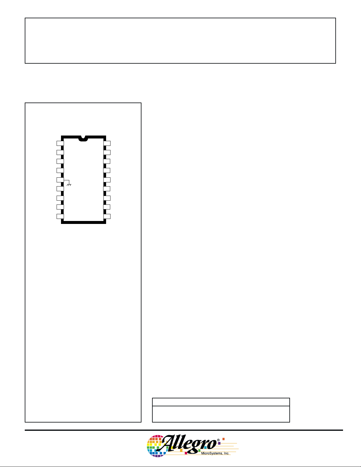
MODE SELECT
MODE SELECT
STEP IN
RESET
GROUND
MONITOR OUT
SHIFT CLOCK
SERIAL DATA OUT
STROBE OUT
1
1
2
2
3
4
5
6
7
8
9
A4255CA
DD
18
MODE SELECT
DIRECTION
17
CONTROL IN
16
OSC/CLOCK IN
15
OSC/CLOCK OUT
14
SUPPLYV
13
PFD
12
PHASE
11
PFD
10
PHASE
A
A
B
B
Dwg. PP-071A
4255
MICROCONTROLLER
The A4255CA and A4255CLN microcontrollers make designing
with step motors easy, inexpensive, and productive. A reference design
technique is integral to the implementation of a system that includes the
power circuitry, a low-cost, 8-bit, preprogrammed microcontroller and
the other components needed to complete the control hardware. The
0
A4255Cx eliminates the need for software development, expedites the
product creation, and hastens the time to market.
The reference design can be utilized directly or integrated into a
larger printed wiring board. A further benefit is the compactness of the
circuit layout. Power-driver output ratings presently available with these
devices are 50 V and ±1.5 A (with the A3955 or A3957). A similar
device for 46 V and either 1.5 A (with the SLA7042M) or 3 A (with the
SLA7044M) is planned. The reference design supports stepping formats
that include full-step, half-step, quarter-step, eighth-step, and sixteenthstep (microstepping) increments for a two-phase stepping motor.
The A4255CA is furnished in an 18-pin dual in-line plastic package
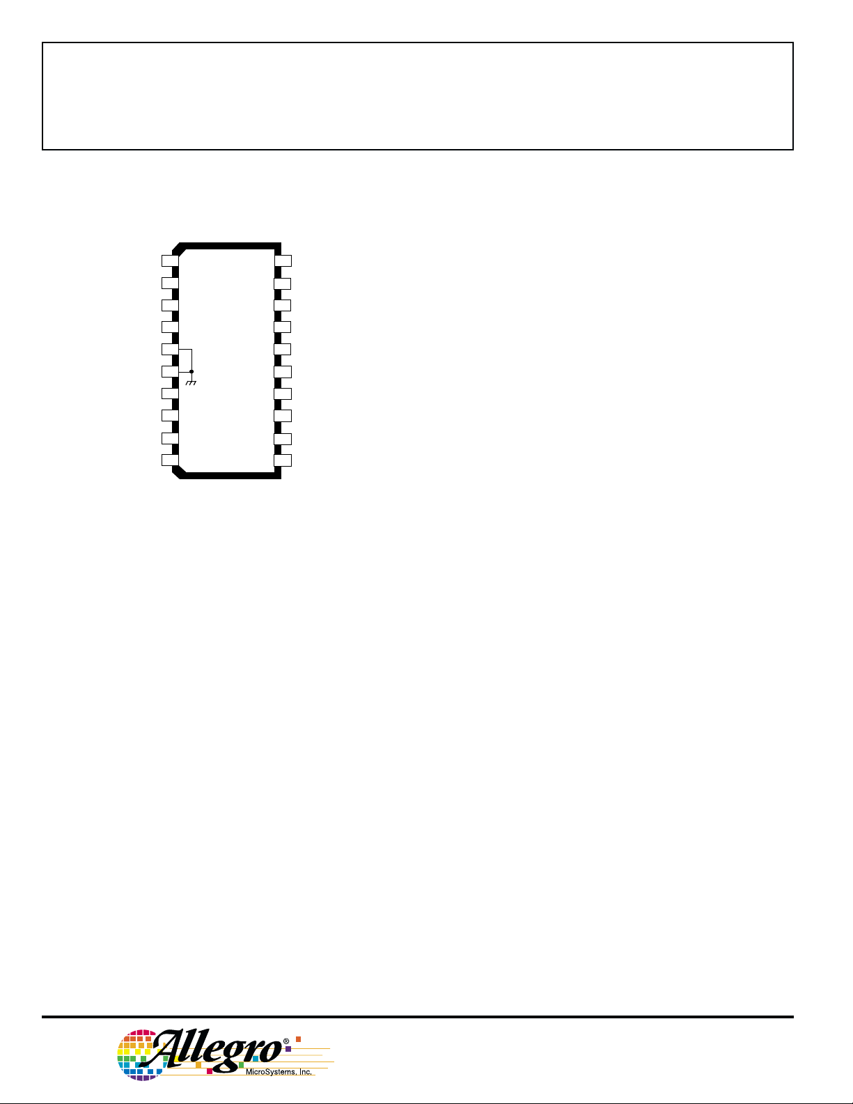
for through-hole applications. The A4255CLN is furnished in a 20-lead
wide-body, shrink-pitch, small-outline plastic package (SSOP) with gullwing leads for minimum area, surface-mount applications.
26113
8-BIT
ABSOLUTE MAXIMUM RATINGS
Supply Voltage, VDD.......................... 7.0 V
Input Voltage Range,
VI........................ -0.3 V to VDD + 0.6 V
RESET Voltage, V
Input Clamp Current, IIK............... ±20 mA
Output Clamp Current, IOK............ ±20 mA
Operating Temperature Range,
TA.................................... 0°C to +70°C
Storage Temperature Range,
TS.............................. -55°C to +150°C
Caution: These CMOS devices have input
static protection (Class 3) but are still
susceptible to damage if exposed to extremely
high static electrical charges.
...................... 14 V
RESET
FEATURES
■ Full-, Half-, Quarter-, Eighth-, or Sixteenth-Step Increments
■ DC to 20 MHz Clock Input
■ Power-On Reset
■ Brown-Out Reset
■ High-Speed CMOS Technology
■ Low Power, <20 mA @ 5 V, 20 MHz
(Typically 9 mA)
Always order by complete part number:
Part Number Package
A4255CA 18-pin DIP
A4255CLN 20-lead shrink-pitch SOIC
Page 2
4255
8-BIT
MICROCONTROLLER
A4255CLN
0.65 mm (0.026”) pitch
MODE SELECT
MODE SELECT
STEP IN
RESET
GROUND
GROUND
MONITOR OUT
SHIFT CLOCK
SERIAL DATA OUT
STROBE OUT
1
1
2
2
3
4
5
7
9
8
9
10
DD
DD
MODE SELECT
20
DIRECTION
19
CONTROL IN
18
OSC/CLOCK IN
17
OSC/CLOCK OUT
SUPPLYV
16
156
SUPPLYV
14
PFD
13
PHASE
PFD
12
PHASE
11
0
A
A
B
B
Dwg. PP-071-1
FUNCTIONAL DESCRIPTION
To ease and simplify the design effort, the user only
provides the following signals: (a) direction, (b) stepping
clock (8x the full-step frequency), (c) mode logic (three
inputs determine the operation for full, half, quarter, or
eighth stepping), (d) reset input (initiates a ‘detent’
position), and (e) recirculation control (this allows establishing the percent of fast- vs slow-decay in the phase
winding). The microcontroller program providess automatic recirculation control. This eliminates the need for
evaluating the impact of stepping rate vs the sinusoidal
current profile.
Although recirculation control can provide slight
improvements (i.e., lower current ripple, reduced motor
heating [a few degrees], and diminish audible noise levels
[minimal differences]), this entails an evaluation of the
motor (and step frequencies) to determine the proper ratio
of fast- and slow-decay. The benefits of tuning the
recirculation ratios are small, and the time and effort
required can be considerable. Hence, the uninitiated user
should opt for the automatic recirculation control, and
avoid the essentially unnecessary activity.
RECOMMENDED OPERATING CONDITIONS
over operating temperature range
Logic Supply Voltage Range, VDD............... 4.5 V to 5.5 V
High-Level Input Voltage, VIH............................ ≥ 0.85V
Low-level input voltage, VIL................................. ≤0.15V
MICROCONTROLLER OPERATION
Although ‘hardware’ control of the microstepping ICs
is feasible, without a specific (ASIC), monolithic IC
controller the prime solution becomes a ‘software’ option.
From the user’s perspective, a ‘preprogrammed’ microcontroller appears little, or no, different than a ‘dedicated’
controller and sequencer IC expressly created for microstepping applications of the power-driver ICs. Further,
the flexibility of a software-based drive is certainly a basic
benefit (high-volume production of 8-bit microcontrollers
transposes to low-cost circuitry).
As an indicator of the logic signals needed to control
the power ICs, Table 1 lists the required A3955 inputs to
the 3-bit DAC for eighth-step operation (the similar
A3957 uses a 4-bit DAC for sixteenth-step operation).
These I/O signals are serial data from the microcontroller,
then converted to a parallel mode by a 74HC595 as the
‘interface’ between the microcontroller and the two
microstepping power ICs.
The versatility offered by software control allows the
operating modes listed in Table 1. This table itemizes the
various logic inputs that determine direction, stepping
DD
DD
115 Northeast Cutoff, Box 15036
Worcester, Massachusetts 01615-0036 (508) 853-5000
Copyright © 2000, Allegro MicroSystems, Inc.
Page 3

FUNCTIONAL DESCRIPTION (cont’d)
format, reset, 1/8th vs 1/16th sub-steps, etc. Note that
during power up, shift clock (SCLK) is sampled for a pullup or pull-down resistor to establish the fractional step
limit. A pull up sets up a 1/8th-step format (for the
A3955) and pull down sets up 1/16th-operation (for the
A3957).
Table 2 lists the microcontroller terminal descriptions
and provides the essence of the circuit operation (a
schematic illustrating a typical stepper design follows). A
brief description of the microcontroller I/O should clarify
the connections of the various elements of the drive
electronics.
4255
8-BIT
MICROCONTROLLER
Table 1 — Controller/sequencer IC operational logic
Binary inputs Operating mode Comments
DIR MS2 MS1 MS0 (Command executed on L → H of CLK) (Applicable power ICs)
0000 CW, Full step (single-phase) A3955/57
0001 CW, Half step (constant torque) A3955/57
0010 CW, 1/4 step (constant torque) A3955/57
0011 CW, 1/8th step (constant torque) A3955/57
0100 CW, 1/16th step (constant torque) A3957 only
0101 Disable A3955/57 holding torque At present position
0110 Enable A3955/57 holding torque From present position
0111 Reset A4255 sequencer IC A3955/57
1000 CCW, full step (single-phase) A3955/57
1001 CCW, half step (constant torque) A3955/57
1010 CCW, 1/4 step (constant torque) A3955/57
1011 CCW, 1/8th step (constant torque) A3955/57
1100 CCW, 1/16th step (constant torque) A3957 only
1101 Disable A3955/57 holding torque At present position
1110 Enable A3955/57 holding torque From present position
1111 Reset A4255 sequencer IC A3955/57
www.allegromicro.com
Page 4

4255
8-BIT
MICROCONTROLLER
FUNCTIONAL DESCRIPTION (cont’d)
Table 2 — Microcontroller terminal descriptions
A4255CA A4255CLN
DIP SSOP Function Description Comments, connections, etc.
1 1 Input Mode select 1 Static and/or dynamic control of stepping mode
2 2 Input Mode select 2 Static and/or dynamic control of stepping mode
3 3 Input Step in Governs full-step rate (÷8 for A3955; ÷16 for A3957)
4 4 Input Reset Resets DIR., MS2, MS1, and MS0 to 0000 (detent)
5 5, 6 Power Ground Logic power return
6 7 Output Monitor out Signals full-step rotor alignment (active low)
7 8 I/O Shift clock Pull up for A3955; pull down for A3957
8 9 Output Serial data out Shifts 8-bit serial data to 74HC595 serial input
9 10 Output Strobe out Latches 8-bit data into 74HC595 (latch clock in)
10 11 Output Phase B Controls current direction in phase B
11 12 Output PFD B Phase B recirculation control
12 13 Output Phase A Controls current direction in phase A
13 14 Output PFD A Phase A recirculation control
14 15, 16 Power Supply (V
15 17 Output Osc/clock out Crystal oscilator connection
16 18 Input Osc/clock in Crystal oscillator connection/external clock input
17 19 Input Direction control Determines direction of step motor rotation
18 20 Input Mode select 0 Static and/or dynamic control of stepping mode
) Recommended range: 4.5 V to 5.5 V
DD
Mode-select inputs
These three inputs (MS2, MS1, and MS0) determine
the stepping format, disable/enable motor power, and reset
the controller/sequencer. In conjunction with the direction
input, the mode inputs control the sixteen operating states
listed. Deactivating stepper power in any position except
‘detent’ (i.e., a single phase activated) results in the motor
rotor advancing, or retracting, from its intermediate
position and alignment with a natural (i.e., minimumreluctance flux field) orientation. The absolute position
may be affected by inertia, load, fractional position,
ringing, etc. and cannot be determined without feedback.
Phase currents must be maintained to immobilize the
rotor/load in any intermediate position.
115 Northeast Cutoff, Box 15036
Worcester, Massachusetts 01615-0036 (508) 853-5000
Step (clock) input
The sequencer stepping-clock frequency is a multiple
of the actual stepping rate. The A3955 requires a stepping-clock input frequency equal to eight times the
intended stepping rate for the motor; the A3957 requires a
stepping clock rate that is sixteen times the actual stepping
rate of the motor. However, neither design necessitates
that the step frequency be varied should the operating
mode(s) be switched during operation. Shifting from one
stepping format does not mandate a simultaneous (and
equivalent) change in the clock frequency.
Using a 20 MHz crystal (maximum limit for the
A4255) allows a 50 kHz stepping clock for the A3955,
and this equates to 6 250 full steps per second (50 kHz/8).
For the A3957 this 50 kHz stepping clock translates to
Page 5

MICROCONTROLLER
FUNCTIONAL DESCRIPTION (cont’d)
4255
8-BIT
3 125 full steps per second (50 kHz/16). These frequencies represent the attainable limits with the A4255.
Although not a necessity, a stepping clock with a 50%
duty cycle represents the simplest technique for providing
an appropriate (≤50 kHz) stepping clock rate. The step
clock varies depending upon the start, acceleration,
slewing, deceleration, and stop trajectories mandated by
the motion system control and ‘point-to-point’ timing
objectives.
Reset input
The preprogrammed microcontroller incorporates two
‘software’ reset states that are serially loaded with MS2,
MS1, and MS0 all high. However, the direct hardware
reset is actuated with a logic 0 (active low) on this input
An input low level defaults to the 0000 binary state and
sets the rotor to its natural (or detent) position with onephase energized.
Monitor output
An output low signal indicates a rotor alignment
corresponding to a single phase on position. Any changes
in the operating mode (microstepping to full-step, etc.)
should coincide with the interval that the monitor output is
in the low state. This alleviates noise problems, excessive
ringing, etc. that may result from changing the stepping
modes on-the-fly. Nonlinear (such as S-curve) acceleration profiles can exploit this signal to achieve very
smooth, quiet stepper operation.
Shift clock output
This I/O terminal serves a dual purpose. On power
up, the microcontroller samples this terminal as an input.
Connecting a pull-up resistor results in 1/8th-step format;
while a pull-down resistor configures the controller for its
1/16th-step mode (A3957 only). This provides versatility,
simplicity, and cost-effectiveness for most users.
Operating in its output mode, this I/O constitutes the
shift clock signal for the 74HC595. Data is transferred
from the microcontroller serial-data output to the serialdata input of the 74HC595. This 8-bit serial format is
converted into parallel signals controlling the 3-bit (or 4-
bit) DAC input lines to the two microstepping power ICs.
Serial data from the serial data output is valid on the lowto-high clock transitions and eight clock pulses shift serial
control signals into the 74HC595. A basic timing diagram
(showing serial data, shift clock, and strobe) is depicted.
Signal timing is controlled by the preprogrammed microcontroller; data entered into the 74HC595 shift register is
then latched by the low-to-high transition of the strobe
input.
SDO
SCLK
ST
D7 D6 D5 D4 D3 D2 D1 D0
Dwg. WP-040A
Serial data, shift clock, and strobe
Serial data output
The binary signal instructions that control each of the
microstepping power ICs is shown in table 1. The first
3-bits (or 4-bits) control the digital-to-analog conversion
in one power IC, while the next 3 (or 4-bits) ratio the
second power driver current. The microcontroller monitors all the various static inputs (i.e., Direction, Mode
Selects, Reset), and by exploiting the Stepping Clock for
its input frequency, transfers the 8-bit data commands to
the power driver ICs via the serial-to-parallel interface IC.
The microcontroller utilizes look-up tables to provide
overall control of direction, stepping format, and recirculation mode (PFD). The microcontroller reads inputs and
then outputs time-based signals to control both microstepping ICs.
Strobe output
After the 8-bit serial data has been loaded into the
shift register, a low-to-high transition on the strobe output
transfers the serial data from the shift register into the
eight ‘D’ flip-flops that compose the parallel-data outputs.
This ‘latched’ data controls microstepping current ratios
for both power ICs, and is ‘updated’ after eight step
clocks.
www.allegromicro.com
Page 6

4255
8-BIT
MICROCONTROLLER
FUNCTIONAL DESCRIPTION (cont’d)
Direction control outputs
Two of the microcontroller outputs are devoted to
direction control. The direction signals follow the sequencing to provide the 1/8th-step ‘sinusoidal’ waveforms. Direction outputs are parallel, and connected
directly to the power IC inputs (A3955 in the schematic).
Obviously, both direction signals must coincide with the
8-bit serial-to-parallel conversion signals that control the
phase current ratios (D2, D1, and D0).
PFD control outputs
Another pair of microcontroller outputs constitute
parallel, direct control of the recirculation paths during
each PWM current cycle. The percentage of fast-decay
(or four-quadrant) to slow-decay (or two-quadrant)
recirculation determines how effectively the output current
tracks a sinusoidal waveform. Mixed-mode operation was
utilized for those portions of each microstepping cycle in
which the current is decreasing. The application of
mixed-mode decay allows the PWM current to properly
decay during each fixed-off-time interval.
The typical application shown includes a pair of
49.9 kΩ variables and allows setting the ratios of fast- and
slow-decay to match the individual characteristics of the
step motor, step frequency, supply voltage, etc. As the
stepping frequency is increased, waveform anomalies
become more pronounced, and the benefit of mixed mode
(or fast decay) also becomes very noticeable.
A comprehensive discussion of mixed-mode operation
is included in Allegro Technical Paper STP 97-5.
Oscillator input/clock input
This device connection serves as one terminal for a
parallel-cut crystal (oscillator 2 is the other). In the
typical application, two 20 pF capacitors are recommended, and a series resistor from oscillator out may be required if AT-cut crystals are utilized.
Also, this terminal is used if an external clock (from a
system computer, etc.) is connected here in lieu of a
crystal or ceramic resonator. If so, the oscillator out
connection is left open. The 20 MHz frequency limit
applies to using any clock source.
Oscillator output/clock output
This is the other device connection used for the
internal crystal oscillator (or ceramic resonator) that
supplies the microcontroller with an oscillator/time base
(≤20 MHz).
Direction input
This input controls the sequencing of the winding
currents. Reversing direction may necessitate deceleration
(perhaps full stop) to avoid problems associated with the
load inertia causing the motor to overshoot the proposed
stop/reverse position.
A more extensive discussion of this microcontoller
and microstepping is included in Allegro Technical Paper
STP 99-11.
CONTROL OF PHASE CURRENTS
The power-driver ICs regulate the winding currents,
and the user establishes the design value via a stable
voltage reference and a current-sensing resistor for each
winding (R
and R19).
8
115 Northeast Cutoff, Box 15036
Worcester, Massachusetts 01615-0036 (508) 853-5000
Page 7

4255
VCC
REF
D2
D1
D0
PFD
PHASE
RC
GND
GND
GND
VBB
OUTA
OUTB
SENSE
GND
A3955
STEP
MS2
MS1
MS0
DIR
MON
SCLK
SDO
ST
VCC
SCLR
RCK
SER
SCK
G
GND
Q'H
QH
QG
QF
QE
QD
QC
QB
QA
OSC IN
OSC OUT
PFDA
PHASEA
R
VDD
GND
PFDB
PHASEB
CLK
MS2
MS1
MS0
DIR
A3955
A3957
A4255
74HC595
VCC
REF
D0
D1
D2
PFD
PHASE
RC
GND
GND
GND
VBB
OUTA
OUTB
SENSE
GND
A3955
D3B A3957
D3A A3957
SDO
+5 V
+5 V
+5 V
+5 V
+5 V
+5 V
+5 V
10 kΩ50 kΩ
33 kΩ
22 pF
22 pF
10 kΩ (5)
10 kΩ
10 kΩ
4.99 kΩ
10 kΩ
470 pF
39 kΩ
0.56 Ω
0.56 Ω
100 kΩ
0.1 µF
470 pF
39 kΩ
20 MHz
+5 V
10 kΩ
50 kΩ
33 kΩ
+
47 µF
LOAD
SUPPLY
LOAD
SUPPLY
Dwg. EP-068
STEP MOTOR
PHASE A
STEP MOTOR
PHASE B
47 µF
+
8-BIT
MICROCONTROLLER
www.allegromicro.com
Low-cost microstepping drive circuitry
This “typical” application is available as a product evaluation kit (APEK3955SLB-02)
Page 8

4255
8-BIT
MICROCONTROLLER
The products described here are manufactured under one or more
U.S. patents or U.S. patents pending.
Allegro MicroSystems, Inc. reserves the right to make, from time to
time, such departures from the detail specifications as may be
required to permit improvements in the performance, reliability, or
manufacturability of its products. Before placing an order, the user is
cautioned to verify that the information being relied upon is current.
Allegro products are not authorized for use as critical components
in life-support devices or systems without express written approval.
The information included herein is believed to be accurate and
reliable. However, Allegro MicroSystems, Inc. assumes no responsibility for its use; nor for any infringement of patents or other rights of
third parties which may result from its use.
115 Northeast Cutoff, Box 15036
Worcester, Massachusetts 01615-0036 (508) 853-5000
 Loading...