

Page 1
40MX and 42MX FPGA Families
v6.0
Features
HiRel Features
• Commercial, Industrial, Automotive, and Military
Temperature Plastic Packages
High Capacity
• Single-Chip ASIC Alternative
• 3,000 to 54,000 System Gates
• Up to 2.5 kbits Configurable Dual-Port SRAM
• Commercial, Military Temperature, and MIL-STD-883
Ceramic Packages
• QML Certification
• Ceramic Devices Available to DSCC SMD
• Fast Wide-Decode Circuitry
• Up to 202 User-Programmable I/O Pins
Ease of Integration
• Mixed-Voltage Operation (5.0V or 3.3V for core and
High Performance
• 5.6 ns Clock-to-Out
• 250 MHz Performance
• 5 ns Dual-Port SRAM Access
• 100 MHz FIFOs
• 7.5 ns 35-Bit Address Decode
I/Os), with PCI-Compliant I/Os
• Up to 100% Resource Utilization and 100% Pin
Locking
• Deterministic, User-Controllable Timing
• Unique In-System Diagnostic and Verification
Capability with Silicon Explorer II
• Low Power Consumption
• IEEE Standard 1149.1 (JTAG) Boundary Scan Testing
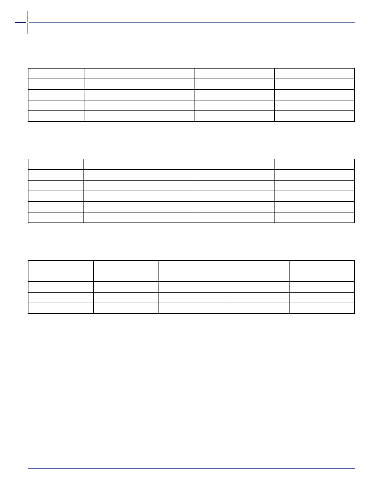
Product Profile
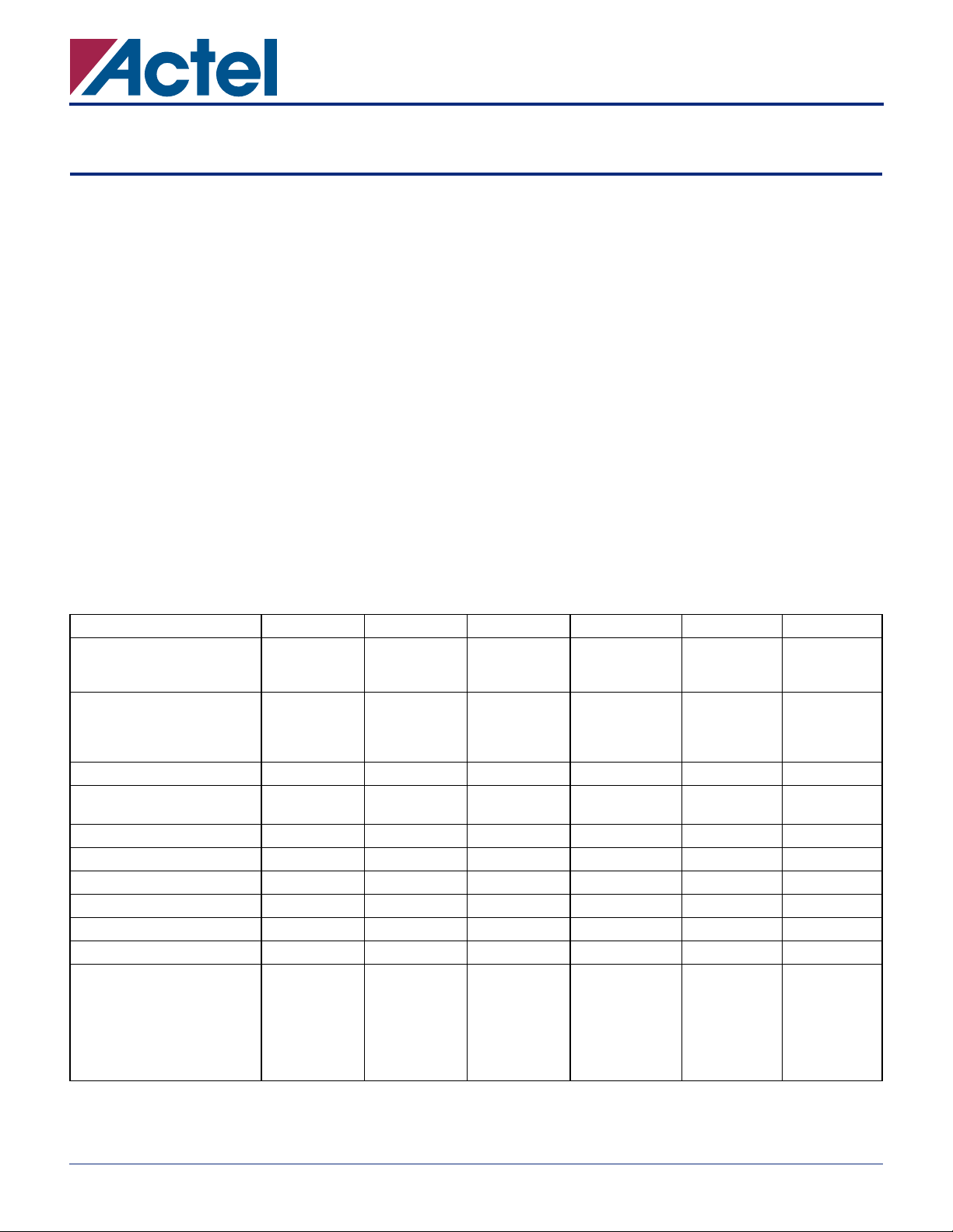
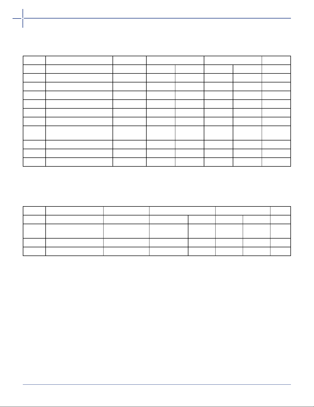
Device A40MX02 A40MX04 A42MX09 A42MX16 A42MX24 A42MX36
Capacity
System Gates
SRAM Bits
Logic Modules
Sequential
Combinatorial
Decode
Clock-to-Out 9.5 ns 9.5 ns 5.6 ns 6.1 ns 6.1 ns 6.3 ns
SRAM Modules
(64x4 or 32x8) ––– – –10
Dedicated Flip-Flops – – 348 624 954 1,230
Maximum Flip-Flops 147 273 516 928 1,410 1,822
Clocks 112 2 26
User I/O (maximum) 57 69 104 140 176 202
PCI ––– –YesYes
Boundary Scan Test (BST) ––– –YesYes
Packages (by pin count)
PLCC
PQFP
VQFP
TQFP
CQFP
PBGA
3,000
–
–
295
–
44, 68
100
80
–
–
–
6,000
–
–
547
–
44, 68, 84
100
80
–
–
–
14,000
–
348
336
–
84
100, 160
100
176
–
–
24,000
–
624
608
–
84
100, 160, 208
100
176
–
–
36,000
–
954
912
24
84
160, 208
–
176
–
–
54,000
2,560
1,230
1,184
24
–
208, 240
–
–
208, 256
272
January 2004 i
© 2004 Actel Corporation See the Actel website (www.actel.com) for the latest version of this datasheet.
Page 2
40MX and 42MX FPGA Families
y
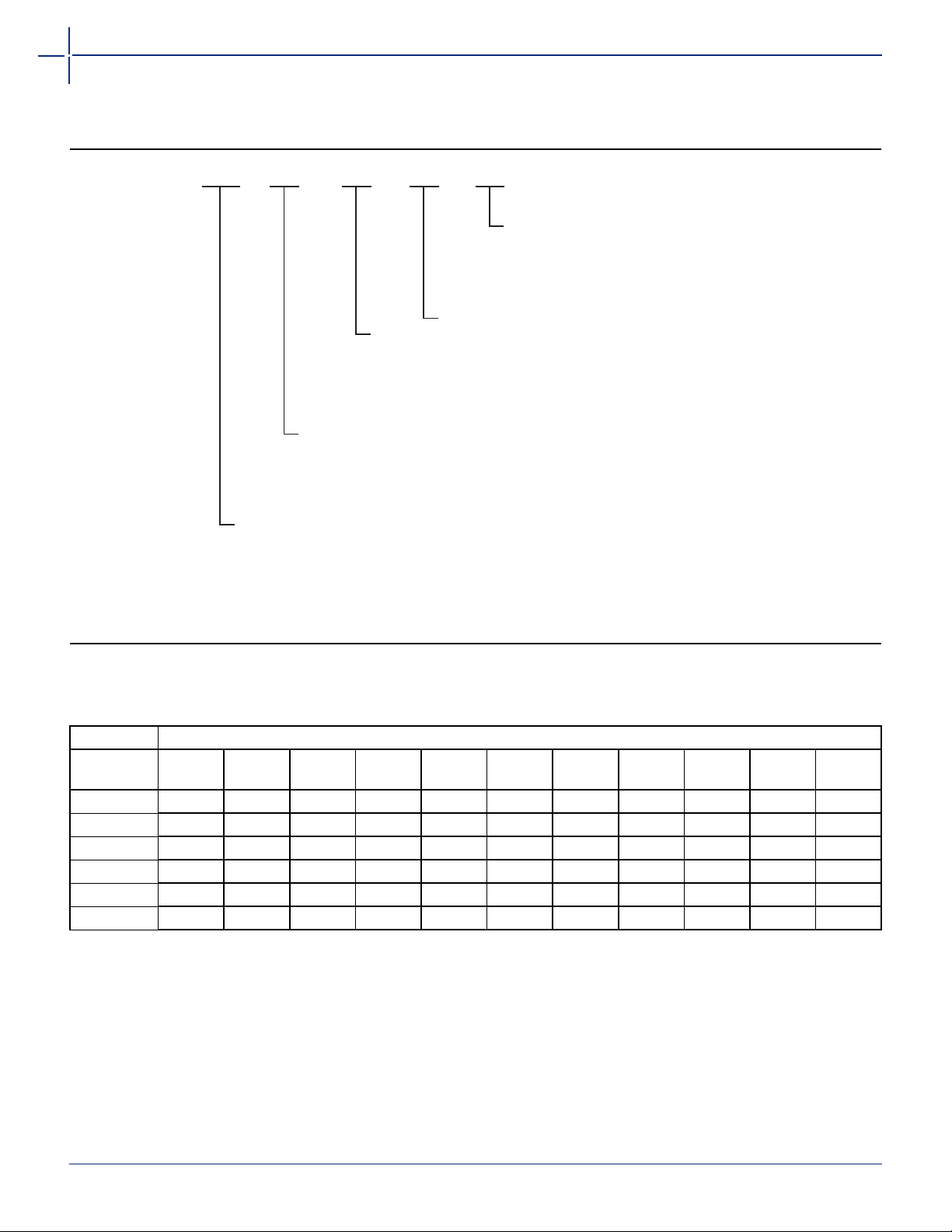
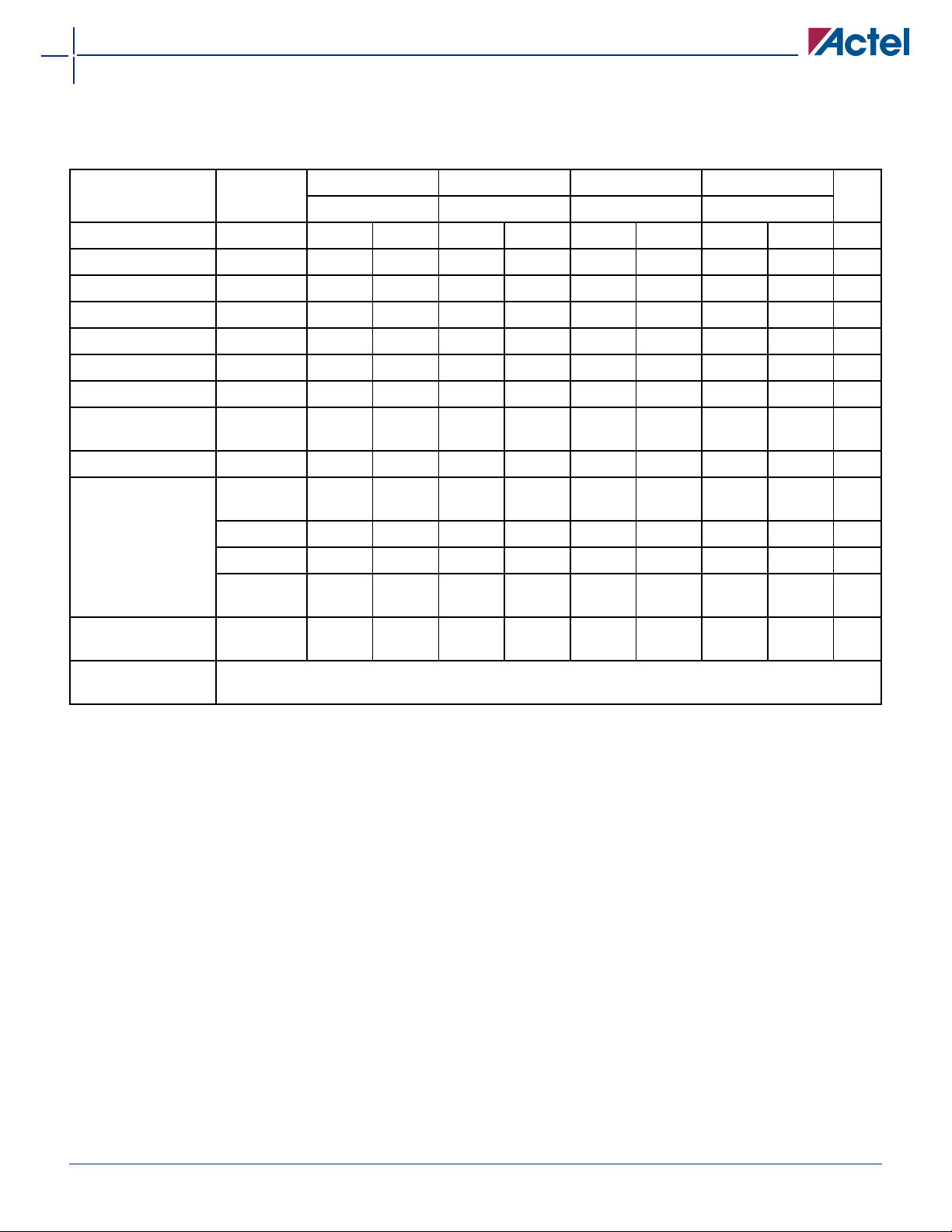
Ordering Information
A42MX16
_
1
Speed Grade
Part Number
A40MX02 = 3,000 System Gates
A40MX04 = 6,000 System Gates
A42MX09 = 14,000 System Gates
A42MX16 = 24,000 System Gates
A42MX24 = 36,000 System Gates
A42MX36 = 54,000 S
PQ 100
Package Lead Count
Package Type
PL = Plastic Leaded Chip Carrier
PQ = Plastic Quad Flat Pack
TQ = Thin (1.4 mm) Quad Flat Pack
VQ = Very Thin (1.0 mm) Quad Flat Pack
BG = Plastic Ball Grid Array
CQ = Ceramic Quad Flat Pack
Blank = Standard Speed
–1 = Approximately 15% Faster than Standard
–2 = Approximately 25% Faster than Standard
–3 = Approximately 35% Faster than Standard
–F = Approximately 40% Slower than Standard
stem Gates
ES
Application (Temperature Range)
Blank = Commercial (0 to +70˚C)
I = Industrial (–40 to +85˚C)
M = Military (–55 to +125˚C)
B = MIL-STD-883
A = Automotive (–40 to +125˚C)
Plastic Device Resources
User I/Os
PLCC
Device
44-Pin
A40MX02 34 57 – 57 – – – 57 – – –
A40MX04 34 57 69 69 – – – 69 – – –
A42MX09 – – 72 83 101 – – – 83 104 –
A42MX16 – – 72 83 125 140 – – 83 140 –
A42MX24 – – 72 – 125 176 – – – 150 –
A42MX36–––––176202–––202
Note: Package Definitions
PLCC = Plastic Leaded Chip Carrier, PQFP = Plastic Quad Flat Pack, TQFP = Thin Quad Flat Pack, VQFP = Very Thin Quad Flat Pack,
PBGA = Plastic Ball Grid Array
PLCC
68-Pin
PLCC
84-Pin
PQFP
100-Pin
PQFP
160-Pin
PQFP
208-Pin
PQFP
240-Pin
VQFP
80-Pin
VQFP
100-Pin
TQFP
176-Pin
PBGA
272-Pin
ii v6.0
Page 3
40MX and 42MX FPGA Families
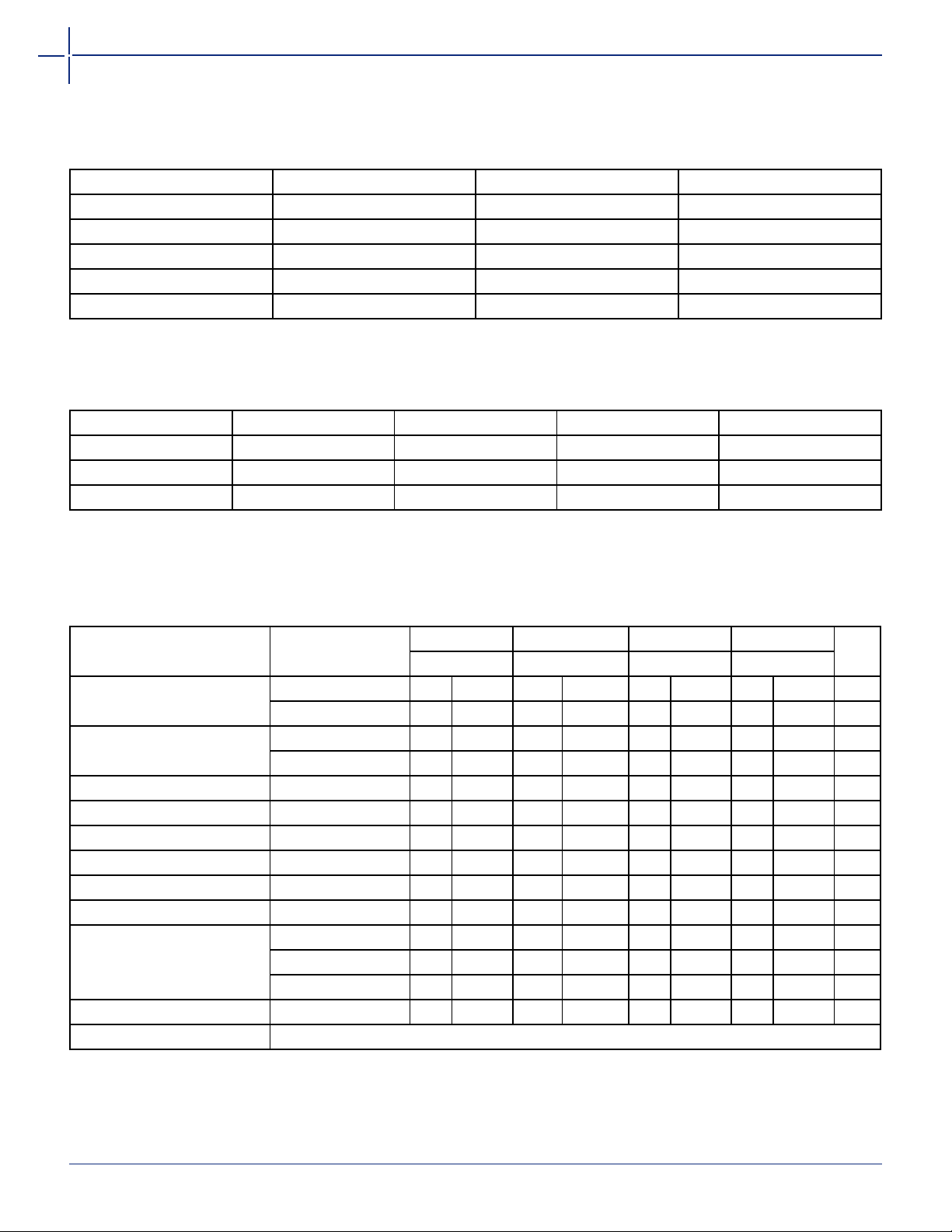
Ceramic Device Resources
User I/Os
Device CQFP 208-Pin CQFP 256-Pin
A42MX36 176 202
Note: Package Definitions CQFP = Ceramic Quad Flat Pack
Temperature Grade Offerings
Package A40MX02 A40MX04 A42MX09 A42MX16 A42MX24 A42MX36
PLCC 44 C, I, M C, I, M
PLCC 68 C, I, A, M C, I, M
PLCC 84 C, I, A, M C, I, A, M C, I, M C, I, M
PQFP 100 C, I, A, M C, I, A, M C, I, A, M C, I, M
PQFP 160 C, I, A, M C, I, M C, I, A, M
PQFP 208 C, I, A, M C, I, A, M C, I, A, M
PQFP 240 C, I, A, M
VQFP 80 C, I, A, M C, I, A, M
VQFP 100 C, I, A, M C, I, A, M
TQFP 176 C, I, A, M C, I, A, M C, I, A, M
PBGA 272 C, I, M
CQFP 208 C, M, B
CQFP 256 C, M, B
Note:
C = Commercial
I = Industrial
A = Automotive
M = Military
B = MIL-STD-883 Class B
Speed Grade Offerings
– F Std–1–2–3
C ✓✓✓✓✓
I ✓✓✓✓
A ✓
M ✓✓
B ✓✓
Note: Refer to the 40MX and 42MX Automotive Family FPGAs datasheet for details on automotive-grade MX offerings.
Contact your local Actel representative for device availability.
v6.0 iii
Page 4

Page 5

Table of Contents
40MX and 42MX FPGA Families
General Description . . . . . . . . . . . . . . . . . . . . . . . . . . . . . . . . . . . . . . . . . . . . . . . . . . 1-1
MX Architectural Overview . . . . . . . . . . . . . . . . . . . . . . . . . . . . . . . . . . . . . . . . . . . . 1-1
Other Architectural Features . . . . . . . . . . . . . . . . . . . . . . . . . . . . . . . . . . . . . . . . . . . 1-6
Power Dissipation . . . . . . . . . . . . . . . . . . . . . . . . . . . . . . . . . . . . . . . . . . . . . . . . . . . . 1-8
Development Tool Support . . . . . . . . . . . . . . . . . . . . . . . . . . . . . . . . . . . . . . . . . . . 1-13
Related Documents . . . . . . . . . . . . . . . . . . . . . . . . . . . . . . . . . . . . . . . . . . . . . . . . . 1-13
5.0V Operating Conditions . . . . . . . . . . . . . . . . . . . . . . . . . . . . . . . . . . . . . . . . . . . 1-14
5V TTL Electrical Specifications . . . . . . . . . . . . . . . . . . . . . . . . . . . . . . . . . . . . . . . . 1-15
3.3V Operating Conditions . . . . . . . . . . . . . . . . . . . . . . . . . . . . . . . . . . . . . . . . . . . 1-16
3.3V LVTTL Electrical Specifications . . . . . . . . . . . . . . . . . . . . . . . . . . . . . . . . . . . . . 1-17
Mixed 5.0V/3.3V Operating Conditions (for 42MX Devices Only) . . . . . . . . . . . . . 1-18
Mixed 5.0V/3.3V Electrical Specifications . . . . . . . . . . . . . . . . . . . . . . . . . . . . . . . . 1-18
Output Drive Characteristics for 5.0V PCI Signaling . . . . . . . . . . . . . . . . . . . . . . . . 1-19
Output Drive Characteristics for 3.3V PCI Signaling . . . . . . . . . . . . . . . . . . . . . . . . 1-20
Junction Temperature (T
Package Thermal Characteristics . . . . . . . . . . . . . . . . . . . . . . . . . . . . . . . . . . . . . . . 1-22
Timing Models . . . . . . . . . . . . . . . . . . . . . . . . . . . . . . . . . . . . . . . . . . . . . . . . . . . . . 1-23
Parameter Measurement . . . . . . . . . . . . . . . . . . . . . . . . . . . . . . . . . . . . . . . . 1-25
Sequential Module Timing Characteristics . . . . . . . . . . . . . . . . . . . . . . . . . . . . . . . 1-26
Sequential Timing Characteristics . . . . . . . . . . . . . . . . . . . . . . . . . . . . . . . . . . . . . . 1-27
Decode Module Timing . . . . . . . . . . . . . . . . . . . . . . . . . . . . . . . . . . . . . . . . . . . . . . 1-28
SRAM Timing Characteristics . . . . . . . . . . . . . . . . . . . . . . . . . . . . . . . . . . . . . . . . . . 1-28
Dual-Port SRAM Timing Waveforms . . . . . . . . . . . . . . . . . . . . . . . . . . . . . . . . . . . . 1-28
Predictable Performance: Tight Delay Distributions . . . . . . . . . . . . . . . . . . . . . . . 1-30
Timing Characteristics . . . . . . . . . . . . . . . . . . . . . . . . . . . . . . . . . . . . . . . . . . . . . . . 1-30
Temperature and Voltage Derating Factors . . . . . . . . . . . . . . . . . . . . . . . . . . . . . . 1-31
PCI System Timing Specification . . . . . . . . . . . . . . . . . . . . . . . . . . . . . . . . . . . . . . . 1-35
PCI Models . . . . . . . . . . . . . . . . . . . . . . . . . . . . . . . . . . . . . . . . . . . . . . . . . . . . . . . . . 1-35
Timing Characteristics . . . . . . . . . . . . . . . . . . . . . . . . . . . . . . . . . . . . . . . . . . . . . . . 1-36
Pin Descriptions . . . . . . . . . . . . . . . . . . . . . . . . . . . . . . . . . . . . . . . . . . . . . . . . . . . . 1-77
40MX and 42MX FPGA Families
) . . . . . . . . . . . . . . . . . . . . . . . . . . . . . . . . . . . . . . . . . . . . 1-22
J
Package Pin Assignments
44-Pin PLCC . . . . . . . . . . . . . . . . . . . . . . . . . . . . . . . . . . . . . . . . . . . . . . . . . . . . . . . . . 2-1
68-Pin PLCC . . . . . . . . . . . . . . . . . . . . . . . . . . . . . . . . . . . . . . . . . . . . . . . . . . . . . . . . . 2-2
84-Pin PLCC . . . . . . . . . . . . . . . . . . . . . . . . . . . . . . . . . . . . . . . . . . . . . . . . . . . . . . . . . 2-3
v6.0 v
Page 6

40MX and 42MX FPGA Families
Table of Contents
100-Pin PQFP Package . . . . . . . . . . . . . . . . . . . . . . . . . . . . . . . . . . . . . . . . . . . . . . . . 2-6
160-Pin PQFP Package . . . . . . . . . . . . . . . . . . . . . . . . . . . . . . . . . . . . . . . . . . . . . . . . 2-9
208-Pin PQFP Package . . . . . . . . . . . . . . . . . . . . . . . . . . . . . . . . . . . . . . . . . . . . . . . 2-13
240-Pin PQFP Package . . . . . . . . . . . . . . . . . . . . . . . . . . . . . . . . . . . . . . . . . . . . . . . 2-17
80-Pin VQFP . . . . . . . . . . . . . . . . . . . . . . . . . . . . . . . . . . . . . . . . . . . . . . . . . . . . . . . . 2-20
100-Pin VQFP Package . . . . . . . . . . . . . . . . . . . . . . . . . . . . . . . . . . . . . . . . . . . . . . . 2-22
176-Pin TQFP Package . . . . . . . . . . . . . . . . . . . . . . . . . . . . . . . . . . . . . . . . . . . . . . . 2-24
208-Pin CQFP . . . . . . . . . . . . . . . . . . . . . . . . . . . . . . . . . . . . . . . . . . . . . . . . . . . . . . . 2-28
256-Pin CQFP . . . . . . . . . . . . . . . . . . . . . . . . . . . . . . . . . . . . . . . . . . . . . . . . . . . . . . . 2-31
272-Pin BGA Package . . . . . . . . . . . . . . . . . . . . . . . . . . . . . . . . . . . . . . . . . . . . . . . . 2-34
Datasheet Information
List of Changes . . . . . . . . . . . . . . . . . . . . . . . . . . . . . . . . . . . . . . . . . . . . . . . . . . . . . . 3-1
Datasheet Categories . . . . . . . . . . . . . . . . . . . . . . . . . . . . . . . . . . . . . . . . . . . . . . . . . 3-2
vi v6.0
Page 7
40MX and 42MX FPGA Families
40MX and 42MX FPGA Families
General Description
Actel's 40MX and 42MX families offer a cost-effective
design solution at 5V. The MX devices are single-chip
solutions and provide high performance while
shortening the system design and development cycle.
MX devices can integrate and consolidate logic
implemented in multiple PALs, CPLDs, and FPGAs.
Example applications include high-speed controllers and
address decoding, peripheral bus interfaces, DSP, and coprocessor functions.
The MX device architecture is based on Actel’s patented
antifuse technology implemented in a 0.45µm triplemetal CMOS process. With capacities ranging from 3,000
to 54,000 system gates, the MX devices provide
performance up to 250 MHz, are live on power-up and
have one-fifth the standby power consumption of
comparable FPGAs. Actel’s MX FPGAs provide up to 202
user I/Os and are available in a wide variety of packages
and speed grades.
Actel’s A42MX24 and A42MX36 devices also feature
MultiPlex I/Os, which support mixed-voltage systems,
enable programmable PCI, deliver high-performance
operation at both 5.0V and 3.3V, and provide a lowpower mode. The devices are fully compliant with the
PCI Local Bus Specification (version 2.1). They deliver
200 MHz on-chip operation and 6.1 ns clock-to-output
performance.
The 42MX24 and 42MX36 devices include system-level
features such as IEEE Standard 1149.1 (JTAG) Boundary
Scan Testing and fast wide-decode modules. In addition,
the A42MX36 device offers dual-port SRAM for
implementing fast FIFOs, LIFOs, and temporary data
storage. The storage elements can efficiently address
applications requiring wide datapath manipulation and
can perform transformation functions such as those
required for telecommunications, networking, and DSP.
All MX devices are fully tested over automotive and
military temperature ranges. In addition, the largest
member of the family, the A42MX36, is available in both
CQ208 and CQ256 ceramic packages screened to MILSTD-883 levels. For easy prototyping and conversion from
plastic to ceramic, the CQ208 and PQ208 devices are pincompatible.
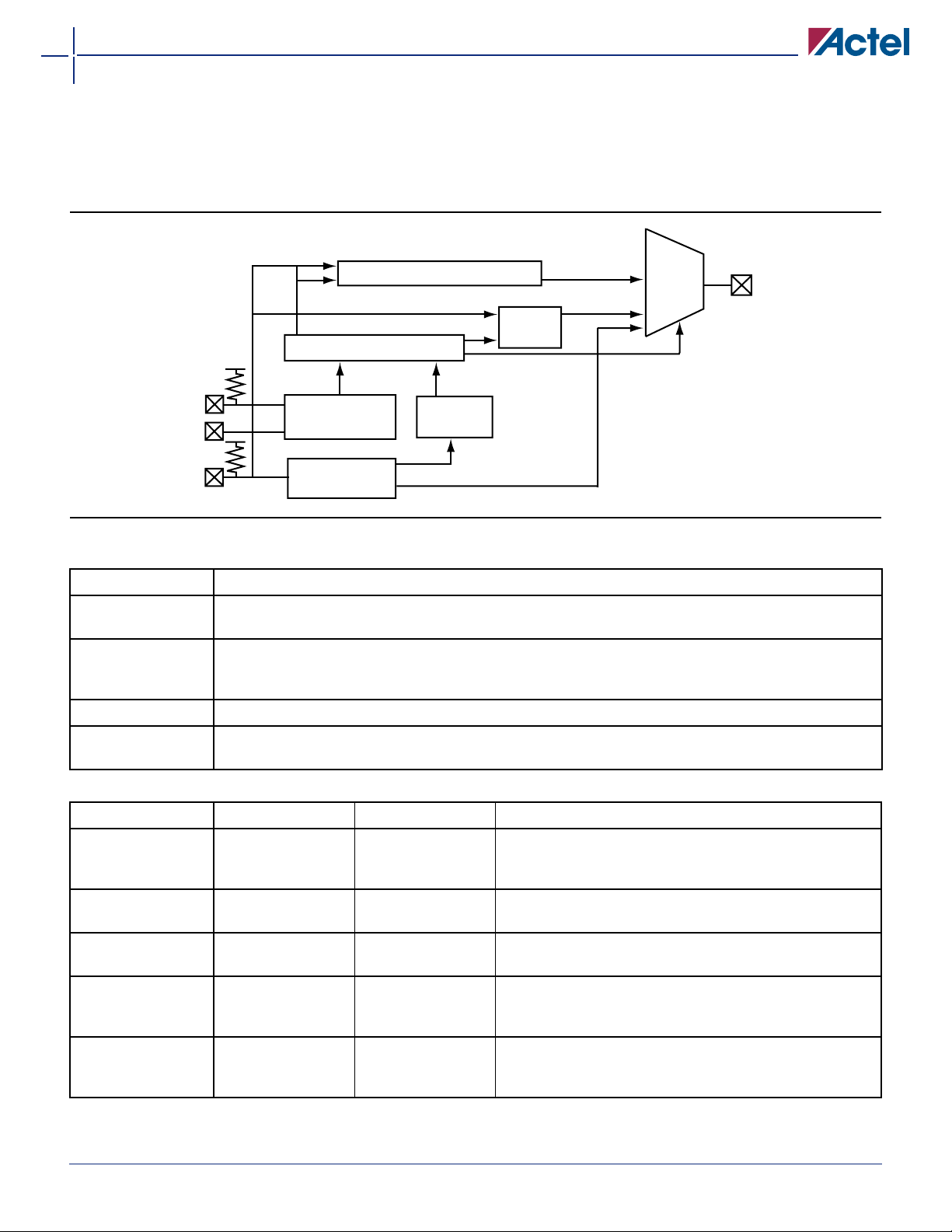
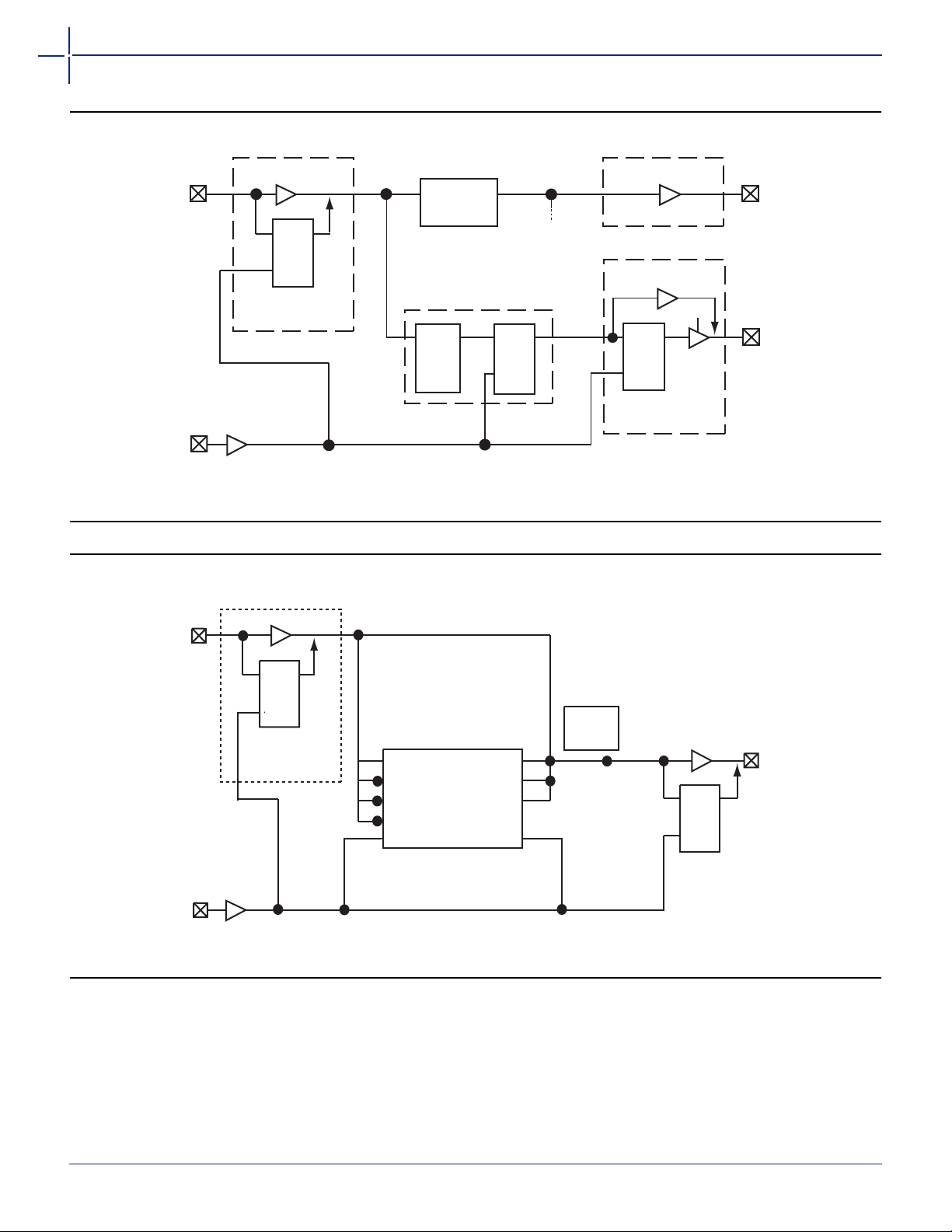
MX Architectural Overview
The MX devices are composed of fine-grained building
blocks that enable fast, efficient logic designs. All devices
within these families are composed of logic modules, I/O
modules, routing resources and clock networks, which
are the building blocks for fast logic designs. In addition,
the A42MX36 device contains embedded dual-port
SRAM modules, which are optimized for high-speed
datapath functions such as FIFOs, LIFOs and scratchpad
memory. A42MX24 and A42MX36 also contain widedecode modules.
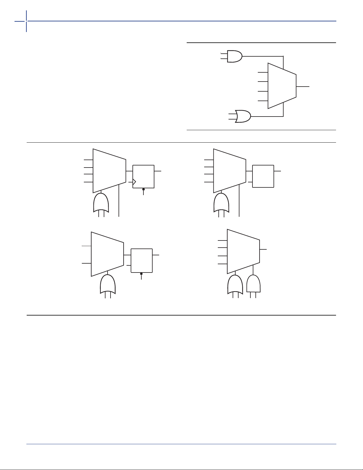
Logic Modules
The 40MX logic module is an eight-input, one-output
logic circuit designed to implement a wide range of logic
functions with efficient use of interconnect routing
resources (Figure 1-1).
The logic module can implement the four basic logic
functions (NAND, AND, OR and NOR) in gates of two,
three, or four inputs. The logic module can also
implement a variety of D-latches, exclusivity functions,
AND-ORs and OR-ANDs. No dedicated hard-wired latches
or flip-flops are required in the array; latches and flipflops can be constructed from logic modules whenever
required in the application.
Figure 1-1 • 40MX Logic Module
v6.0 1-1
Page 8
40MX and 42MX FPGA Families
A
T
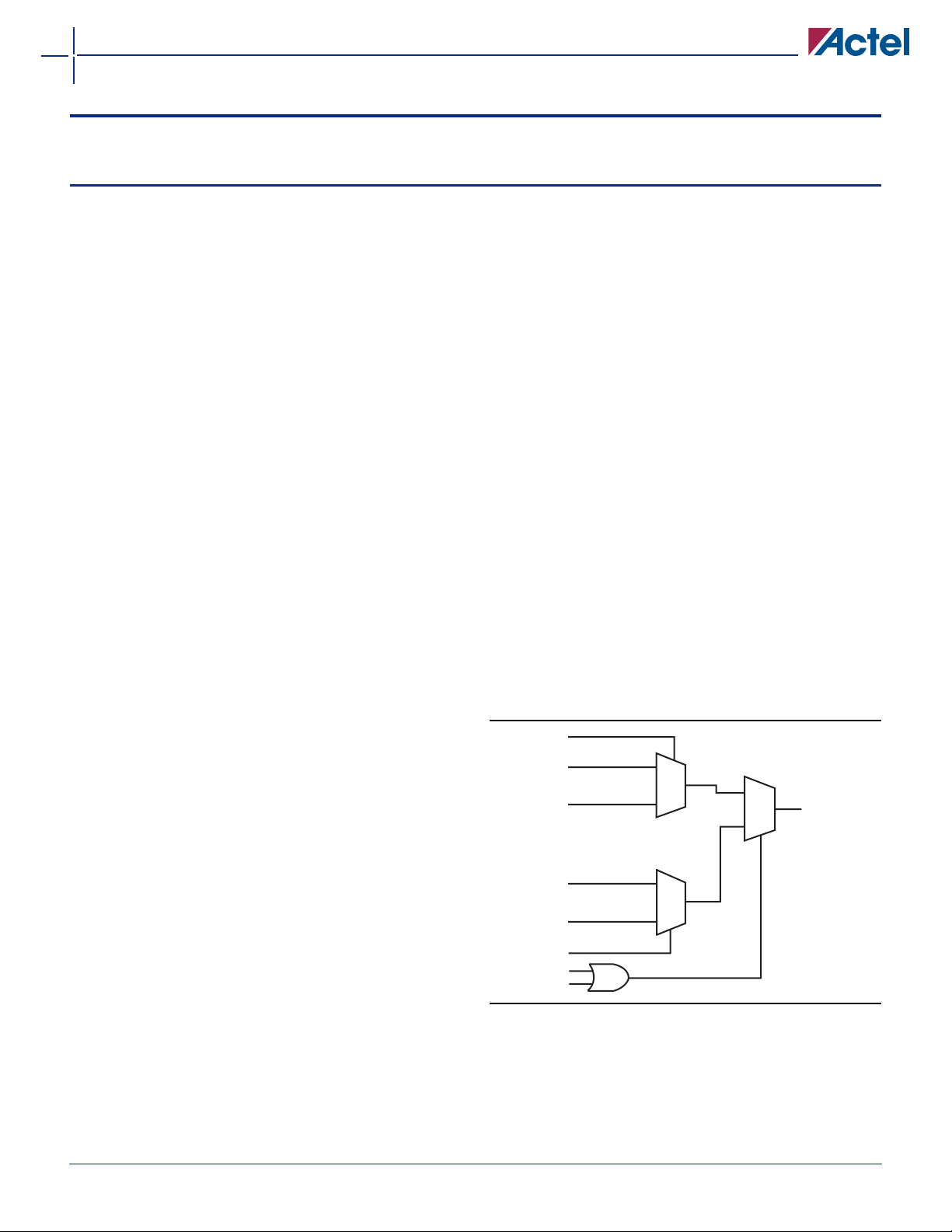
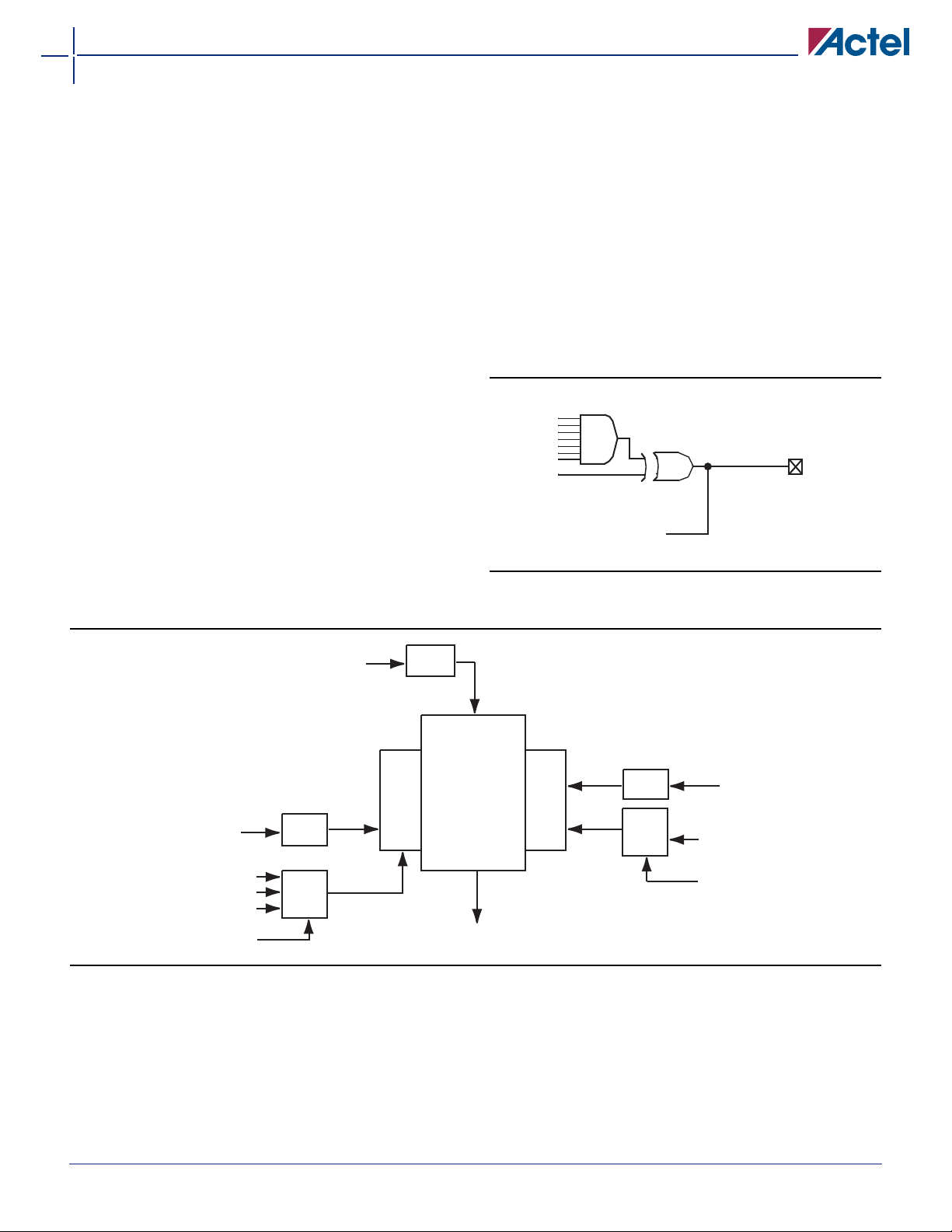
The 42MX devices contain three types of logic modules:
combinatorial (C-modules), sequential (S-modules) and
decode (D-modules). Figure 1-2 illustrates the
combinatorial logic module. The S-module, shown in
Figure 1-3, implements the same combinatorial logic
function as the C-module while adding a sequential
element. The sequential element can be configured as
either a D-flip-flop or a transparent latch. The S-module
register can be bypassed so that it implements purely
combinatorial logic.
0
B0
A1
B1
S0
D00
D01
D10
D11
S1
Figure 1-2 • 42MX C-Module Implementation
Y
D00
D01
D10
D11
S1
Up to 7-Input Function Plus D-Type Flip-Flop with Clear
D0
D1
S
Up to 4-Input Function Plus Latch with Clear
D
Y
S0
D
Y
GATE
Figure 1-3 • 42MX S-Module Implementation
CLR
CLR
Q OUT
Q
OUT
D00
D01
D10
D11
Up to 7-Input Function Plus Latch
Up to 8-Input Function (Same as C-Module)
S0
S1
D00
D01
D10
D11
S1
D
GATE
Y
Q
OUT
Y
S0
OU
1-2 v6.0
Page 9
40MX and 42MX FPGA Families
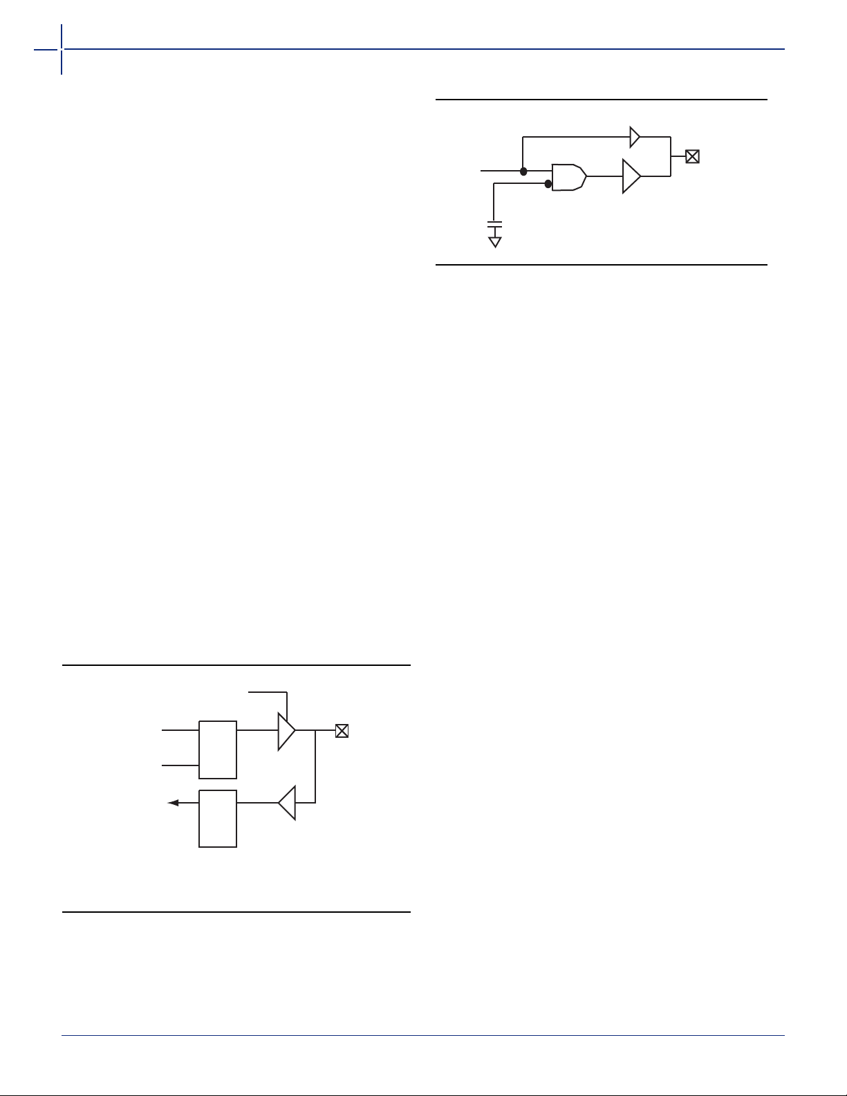
A42MX24 and A42MX36 devices contain D-modules,
which are arranged around the periphery of the device.
D-modules contain wide-decode circuitry, providing a
fast, wide-input AND function similar to that found in
CPLD architectures (Figure 1-4). The D-module allows
A42MX24 and A42MX36 devices to perform widedecode functions at speeds comparable to CPLDs and
PALs. The output of the D-module has a programmable
inverter for active HIGH or LOW assertion. The D-module
output is hardwired to an output pin, and can also be
fed back into the array to be incorporated into other
logic.
Dual-Port SRAM Modules
The A42MX36 device contains dual-port SRAM modules
that have been optimized for synchronous or
asynchronous applications. The SRAM modules are
arranged in 256-bit blocks that can be configured as 32x8
or 64x4. SRAM modules can be cascaded together to
form memory spaces of user-definable width and depth.
A block diagram of the A42MX36 dual-port SRAM block
is shown in Figure 1-5.
The A42MX36 SRAM modules are true dual-port
structures containing independent read and write ports.
Each SRAM module contains six bits of read and write
addressing (RDAD[5:0] and WRAD[5:0], respectively) for
64x4-bit blocks. When configured in byte mode, the
highest order address bits (RDAD5 and WRAD5) are not
used. The read and write ports of the SRAM block
contain independent clocks (RCLK and WCLK) with
programmable polarities offering active HIGH or LOW
implementation. The SRAM block contains eight data
inputs (WD[7:0]), and eight outputs (RD[7:0]), which are
connected to segmented vertical routing tracks.
The A42MX36 dual-port SRAM blocks provide an optimal
solution for high-speed buffered applications requiring
FIFO and LIFO queues. The ACTgen Macro Builder within
Actel's Designer software provides capability to quickly
design memory functions with the SRAM blocks. Unused
SRAM blocks can be used to implement registers for
other user logic within the design.
7 Inputs
Hard-Wire to I/O
Programmable
Inverter
Feedback to Array
Figure 1-4 • A42MX24 and A42MX36 D-Module
Implementation
WD[7:0]
WRAD[5:0]
MOD E
BLKEN
WEN
WCLK
Latches
Write
Logic
[5:0]
Figure 1-5 • A42MX36 Dual-Port SRAM Block
Write
Port
Logic
Latches
[7:0]
SRAM Module
32 x 8 or 64 x 4
(256 Bits)
RD[7:0]
Routing Tracks
Read
Port
Logic
[5:0]
Latches
Read
Logic
RDAD[5:0]
REN
RCLK
v6.0 1-3
Page 10
40MX and 42MX FPGA Families
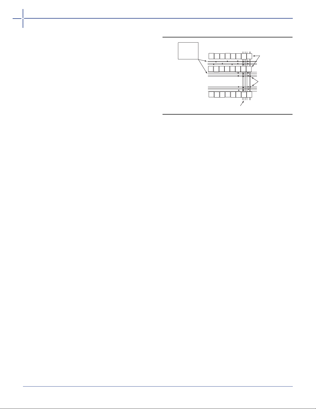
Routing Structure
The MX architecture uses vertical and horizontal routing
tracks to interconnect the various logic and I/O modules.
These routing tracks are metal interconnects that may be
continuous or split into segments. Varying segment
lengths allow the interconnect of over 90% of design
tracks to occur with only two antifuse connections.
Segments can be joined together at the ends using
antifuses to increase their lengths up to the full length of
the track. All interconnects can be accomplished with a
maximum of four antifuses.
Horizontal Routing
Horizontal routing tracks span the whole row length or
are divided into multiple segments and are located in
between the rows of modules. Any segment that spans
more than one-third of the row length is considered a
long horizontal segment. A typical channel is shown in
Figure 1-6. Within horizontal routing, dedicated routing
tracks are used for global clock networks and for power
and ground tie-off tracks. Non-dedicated tracks are used
for signal nets.
Vertical Routing
Another set of routing tracks run vertically through the
module. There are three types of vertical tracks: input,
output, and long. Long tracks span the column length of
the module, and can be divided into multiple segments.
Each segment in an input track is dedicated to the input
of a particular module; each segment in an output track
is dedicated to the output of a particular module. Long
segments are uncommitted and can be assigned during
routing. Each output segment spans four channels (two
above and two below), except near the top and bottom
of the array, where edge effects occur. Long vertical
tracks contain either one or two segments. An example
of vertical routing tracks and segments is shown in
Figure 1-6.
Antifuse Structures
An antifuse is a "normally open" structure. The use of
antifuses to implement a programmable logic device
results in highly testable structures as well as efficient
programming algorithms. There are no pre-existing
connections; temporary connections can be made using
pass transistors. These temporary connections can isolate
individual antifuses to be programmed and individual
circuit structures to be tested, which can be done before
and after programming. For instance, all metal tracks can
be tested for continuity and shorts between adjacent
tracks, and the functionality of all logic modules can be
verified.
Segmented
Horizontal
Routing
Vertical Routing Tracks
Figure 1-6 • MX Routing Structure
Logic
Modules
Antifuses
Clock Networks
The 40MX devices have one global clock distribution
network (CLK). A signal can be put on the CLK network
by being routed through the CLKBUF buffer.
In 42MX devices, there are two low-skew, high-fanout
clock distribution networks, referred to as CLKA and
CLKB. Each network has a clock module (CLKMOD) that
can select the source of the clock signal from any of the
following (Figure 1-7 on page 1-5):
• Externally from the CLKA pad, using CLKBUF
buffer
• Externally from the CLKB pad, using CLKBUF
buffer
• Internally from the CLKINTA input, using CLKINT
buffer
• Internally from the CLKINTB input, using CLKINT
buffer
The clock modules are located in the top row of I/O
modules. Clock drivers and a dedicated horizontal clock
track are located in each horizontal routing channel.
Clock input pads in both 40MX and 42MX devices can
also be used as normal I/Os, bypassing the clock
networks.
The A42MX36 device has four additional register control
resources, called quadrant clock networks (Figure 1-8 on
page 1-5). Each quadrant clock provides a local, high-
fanout resource to the contiguous logic modules within
its quadrant of the device. Quadrant clock signals can
originate from specific I/O pins or from the internal array
and can be used as a secondary register clock, register
clear, or output enable.
1-4 v6.0
Page 11
40MX and 42MX FPGA Families
From
Pads
Figure 1-7 • Clock Networks of 42MX Devices
QCLKA
Quad
QCLKB
*QCLK1IN
Clock
Modul
CLKB
CLKA
Clock
Drivers
QCLK1
CLKMOD
CLKINB
CLKINA
S0
S1
Clock Tracks
QCLK3
Internal
Signal
CLKO(17)
CLKO(16)
CLKO(15)
CLKO(2)
CLKO(1)
Quad
Modul
Clock
QCLKC
QCLKD
*QCLK3IN
S0 S1
Quad
Clock
Modul
*QCLK2IN
S0 S1
QCLK2
QCLK4
Note: *QCLK1IN, QCLK2IN, QCLK3IN, and QCLK4IN are internally-generated signals.
Figure 1-8 • Quadrant Clock Network of A42MX36 Devices
S0S1
Quad
Clock
Modul
*QCLK4IN
S0S1
v6.0 1-5
Page 12
40MX and 42MX FPGA Families
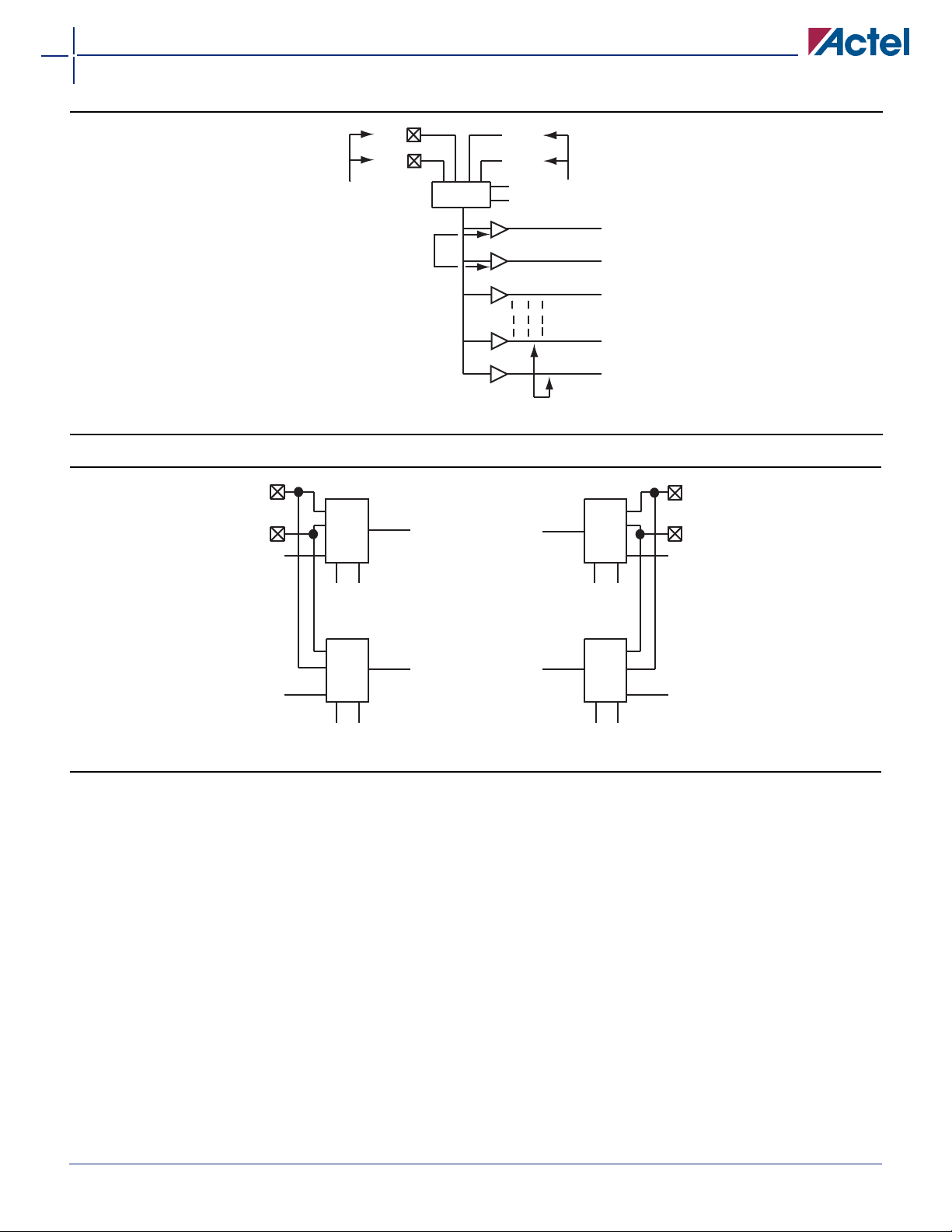
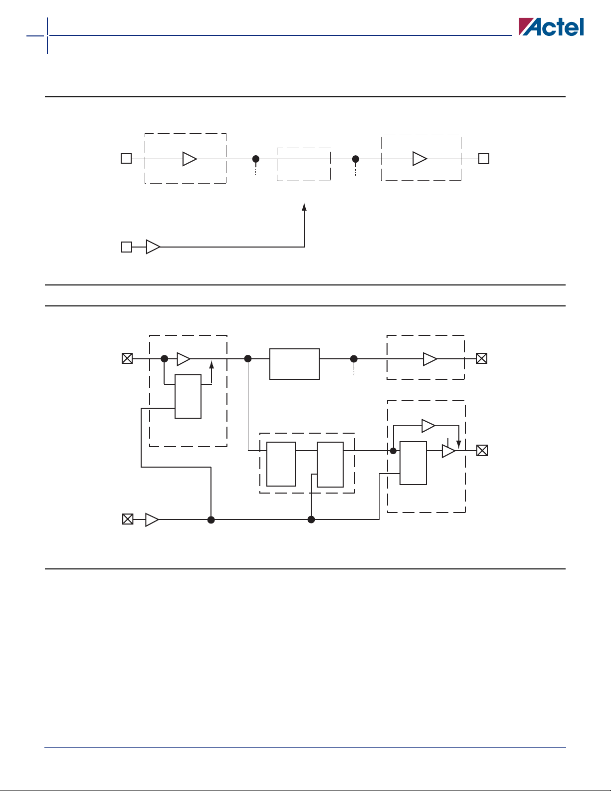
MultiPlex I/O Modules
42MX devices feature Multiplex I/Os and support 5.0V,
3.3V, and mixed 3.3V/5.0V operations.
The MultiPlex I/O modules provide the interface between
the device pins and the logic array. Figure 1-9 is a block
diagram of the 42MX I/O module. A variety of user
functions, determined by a library macro selection, can
be implemented in the module. (Refer to the Antifuse
Macro Library Guide for more information.) All 42MX I/O
modules contain tristate buffers, with input and output
latches that can be configured for input, output, or
bidirectional operation.
All 42MX devices contain flexible I/O structures, where
each output pin has a dedicated output-enable control
(Figure 1-9). The I/O module can be used to latch input or
output data, or both, providing fast set-up time. In
addition, the Actel Designer software tools can build a Dtype flip-flop using a C-module combined with an I/O
module to register input and output signals. Refer to the
Antifuse Macro Library Guide for more details.
A42MX24 and A42MX36 devices also offer selectable PCI
output drives, enabling 100% compliance with version
2.1 of the PCI specification. For low-power systems, all
inputs and outputs are turned off to reduce current
consumption to below 500µA.
To achieve 5.0V or 3.3V PCI-compliant output drives on
A42MX24 and A42MX36 devices, a chip-wide PCI fuse is
programmed via the Device Selection Wizard in the
Designer software (Figure 1-10). When the PCI fuse is not
programmed, the output drive is standard.
Actel's Designer software development tools provide a
design library of I/O macro functions that can implement
all I/O configurations supported by the MX FPGAs.
EN
Q
D
From Array
G/CLK*
To Array
Note: *Can be configured as a Latch or D Flip-Flop (Using
C-Module)
Figure 1-9 • 42MX I/O Module
Q
G/CLK*
D
PAD
STD
Signal
PCI
Drive
PCI Enable
Fuse
Figure 1-10 • PCI Output Structure of A42MX24 and
A42MX36 Devices
Output
Other Architectural Features
Performance
MX devices can operate with internal clock frequencies
of 250 MHz, enabling fast execution of complex logic
functions. MX devices are live on power-up and do not
require auxiliary configuration devices and thus are an
optimal platform to integrate the functionality
contained in multiple programmable logic devices. In
addition, designs that previously would have required a
gate array to meet performance can be integrated into
an MX device with improvements in cost and time-tomarket. Using timing-driven place-and-route (TDPR)
tools, designers can achieve highly deterministic device
performance.
User Security
The Actel FuseLock provides robust security against
design theft. Special security fuses are hidden in the
fabric of the device and prevent unauthorized users from
accessing the programming and/or probe interfaces. It is
virtually impossible to identify or bypass these fuses
without damaging the device, making Actel antifuse
FPGAs immune to both invasive and noninvasive attacks.
Special security fuses in 40MX devices include the Probe
Fuse and Program Fuse. The former disables the probing
circuitry while the latter prohibits further programming
of all fuses, including the Probe Fuse. In 42MX devices,
there is the Security Fuse which, when programmed,
both disables the probing circuitry and prohibits further
programming of the device.
Look for this symbol to ensure your valuable IP is secure.
For more information, refer to Actel's Implementation of
Security in Actel Antifuse FPGAs application note.
1-6 v6.0
Page 13
™
u
e
Figure 1-11 • Fuselock
Programming
Device programming is supported through the Silicon
Sculptor series of programmers. Silicon Sculptor II is a
compact, robust, single-site and multi-site device
programmer for the PC. With standalone software,
Silicon Sculptor II is designed to allow concurrent
programming of multiple units from the same PC.
Silicon Sculptor II programs devices independently to
achieve the fastest programming times possible. After
being programmed, each fuse is verified to insure that it
has been programmed correctly. Furthermore, at the end
of programming, there are integrity tests that are run to
ensure no extra fuses have been programmed. Not only
does it test fuses (both programmed and
40MX and 42MX FPGA Families
nonprogrammed), Silicon Sculptor II also allows self-test
to verify its own hardware extensively.
The procedure for programming an MX device using
Silicon Sculptor II is as follows:
1. Load the .AFM file
2. Select the device to be programmed
3. Begin programming
When the design is ready to go to production, Actel
offers device volume-programming services either
through distribution partners or via In-House
Programming from the factory.
For more details on programming MX devices, please
refer to the Programming Antifuse Devices and the
Silicon Sculptor II user's guides.
Power Supply
MX devices are designed to operate in both 5.0V and
3.3V environments. In particular, 42MX devices can
operate in mixed 5.0V/3.3V systems. Tab le 1 describes the
voltage support of MX devices.
Tabl e 1 • Voltage Support of MX Devices
Device V
40MX 5.0V – – 5.5V 5.0V
42MX – 5.0V 5.0V 5.5V 5.0V
CC
3.3V – – 3.6V 3.3V
– 3.3V 3.3V 3.6V 3.3V
– 5.0V 3.3V 5.5V 3.3V
Power-Up/Down in Mixed-Voltage Mode
When powering up 42MX in mixed voltage mode
(V
=5.0V and V
CCA
or equal to V
V
exceeds V
CCI
protection junction on the I/Os will be forward-biased or
the I/Os will be at logical HIGH, and I
levels. For power-down, any sequence with V
can be implemented.
V
CCI
CCI
throughout the power-up sequence. If
CCI
during power up, either the I/Os' input
CCA
V
CCA
= 3.3V), V
V
CCI
must be greater than
CCA
rises to high
CC
CCA
Maximum Input Tolerance Nominal Output Voltage
Low Power Mode
42MX devices have been designed with a Low Power
Mode. This feature, activated with setting the special LP
pin to HIGH for a period longer than 800 ns, is
particularly useful for battery-operated systems where
battery life is a primary concern. In this mode, the core of
the device is turned off and the device consumes minimal
and
power with low standby current. In addition, all input
buffers are turned off, and all outputs and bidirectional
buffers are tristated. Since the core of the device is
turned off, the states of the registers are lost. The device
must be re-initialized when exiting Low Power Mode. I/
Os can be driven during LP mode, and clock pins should
be driven HIGH or LOW and should not float to avoid
drawing current. To exit LP mode, the LP pin must be
pulled LOW for over 200 µs to allow for charge pumps to
power up, and device initialization will begin.
v6.0 1-7
Page 14

40MX and 42MX FPGA Families
Power Dissipation
The general power consumption of MX devices is made
up of static and dynamic power and can be expressed
with the following equation:
General Power Equation
P = [ICCstandby + ICCactive] * V
+ I
OH
* (V
– VOH) * M
CCI
where:
I
standby is the current flowing when no inputs or
CC
outputs are changing.
active is the current flowing due to CMOS
I
CC
switching.
, IOH are TTL sink/source currents.
I
OL
, VOH are TTL level output voltages.
V
OL
N equals the number of outputs driving TTL loads to
V
.
OL
M equals the number of outputs driving TTL loads to
V
.
OH
Accurate values for N and M are difficult to determine
because they depend on the family type, on design
details, and on the system I/O. The power can be divided
into two components: static and active.
Static Power Component
The static power due to standby current is typically a
small component of the overall power consumption.
Standby power is calculated for commercial, worst-case
conditions. The static power dissipation by TTL loads
depends on the number of outputs driving, and on the
DC load current. For instance, a 32-bit bus sinking 4mA at
0.33V will generate 42mW with all outputs driving LOW,
and 140mW with all outputs driving HIGH. The actual
dissipation will average somewhere in between, as I/Os
switch states with time.
Active Power Component
Power dissipation in CMOS devices is usually dominated
by the dynamic power dissipation. Dynamic power
consumption is frequency-dependent and is a function of
the logic and the external I/O. Active power dissipation
results from charging internal chip capacitances of the
interconnect, unprogrammed antifuses, module inputs,
and module outputs, plus external capacitances due to
PC board traces and load device inputs. An additional
component of the active power dissipation is the totem
pole current in the CMOS transistor pairs. The net effect
can be associated with an equivalent capacitance that
can be combined with frequency and voltage to
represent active power dissipation.
+ IOL* VOL* N
CCI
The power dissipated by a CMOS circuit can be expressed
by the equation:
Power (µW) = CEQ * V
CCA
2
* F(1)
where:
C
=Equivalent capacitance expressed in picofarads (pF)
EQ
V
=Power supply in volts (V)
CCA
F =Switching frequency in megahertz (MHz)
Equivalent Capacitance
Equivalent capacitance is calculated by measuring
active at a specified frequency and voltage for each
I
CC
circuit component of interest. Measurements have been
made over a range of frequencies at a fixed value of
V
CC
Equivalent capacitance is frequency-independent, so the
results can be used over a wide range of operating
conditions. Equivalent capacitance values are shown
below.
CEQ Values for Actel MX FPGAs
Modules (C
Input Buffers (C
Output Buffers (C
Routed Array Clock Buffer Loads (C
To calculate the active power dissipated from the
complete design, the switching frequency of each part of
the logic must be known. The equation below shows a
piece-wise linear summation over all components.
Power = V
(n * C
0.5 * (q
0.5 * (q2 * C
where:
m = Number of logic modules switching at
n = Number of input buffers switching at
p = Number of output buffers switching at
q
= Number of clock loads on the first routed array
1
= Number of clock loads on the second routed
q
2
r
= Fixed capacitance due to first routed array
1
r
= Fixed capacitance due to second routed array
2
)3.5
EQM
EQI
EQO
CCA
* fn)
EQI
* C
1
f
frequency f
frequency f
frequency f
clock
array clock
clock
clock
)6.9
)18.2
2
* [(m x C
+ (p * (C
Inputs
fp)
outputs
* fq1)
EQCR
f
q1)routed_Clk1
* fq2)
EQCR
q2)routed_Clk2
m
n
p
)1.4
EQCR
* fm)
EQM
+
routed_Clk1
routed_Clk2
EQO
+
(2)
+
Modules
+ CL) *
+ (r1 *
+ (r2 *
.
1-8 v6.0
Page 15
40MX and 42MX FPGA Families
= Equivalent capacitance of logic modules in pF
C
EQM
C
= Equivalent capacitance of input buffers in pF
EQI
C
= Equivalent capacitance of output buffers in pF
EQO
C
= Equivalent capacitance of routed array clock in
EQCR
pF
C
= Output load capacitance in pF
L
f
= Average logic module switching rate in MHz
m
f
= Average input buffer switching rate in MHz
n
f
= Average output buffer switching rate in MHz
p
f
= Average first routed array clock rate in MHz
q1
f
= Average second routed array clock rate in MHz
q2
Fixed Capacitance Values for MX FPGAs (pF)
r
2
routed_Clk2
Device Type
r
1
routed_Clk1
A40MX02 41.4 N/A
A40MX04 68.6 N/A
A42MX09 118 118
A42MX16 165 165
A42MX24 185 185
A42MX36 220 220
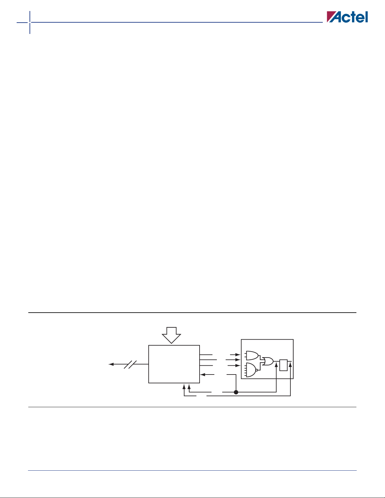
Test Circuitry and Silicon Explorer II Probe
MX devices contain probing circuitry that provides builtin access to every node in a design, via the use of Silicon
Explorer II. Silicon Explorer II is an integrated hardware
and software solution that, in conjunction with the
Designer software, allow users to examine any of the
internal nets of the device while it is operating in a
prototyping or a production system. The user can probe
into an MX device without changing the placement and
routing of the design and without using any additional
resources. Silicon Explorer II's noninvasive method does
not alter timing or loading effects, thus shortening the
debug cycle and providing a true representation of the
device under actual functional situations.
Silicon Explorer II samples data at 100 MHz
(asynchronous) or 66 MHz (synchronous). Silicon Explorer
II attaches to a PC's standard COM port, turning the PC
into a fully functional 18-channel logic analyzer. Silicon
Explorer II allows designers to complete the design
verification process at their desks and reduces
verification time from several hours per cycle to a few
seconds.
Silicon Explorer II is used to control the MODE, DCLK, SDI
and SDO pins in MX devices to select the desired nets for
debugging. The user simply assigns the selected internal
nets in the Silicon Explorer II software to the PRA/PRB
output pins for observation. Probing functionality is
activated when the MODE pin is held HIGH.
Figure 1-12 illustrates the interconnection between
Silicon Explorer II and 40MX devices, while Figure 1-13
on page 1-10 illustrates the interconnection between
Silicon Explorer II and 42MX devices
To allow for probing capabilities, the security fuses must
not be programmed. (Refer to <zBlue>“User Security”
section on page 6 for the security fuses of 40MX and
42MX devices). Table 2 on page 1-10 summarizes the
possible device configurations for probing.
PRA and PRB pins are dual-purpose pins. When the
"Reserve Probe Pin" is checked in the
Designer software, PRA and PRB pins are reserved as
dedicated outputs for probing. If PRA and PRB pins are
required as user I/Os to achieve successful layout and
"Reserve Probe Pin" is checked, the layout tool will
override the option and place user I/Os on PRA and PRB
pins.
16 Logic Analyzer Channels
Serial Connection
to Windows PC
Figure 1-12 • Silicon Explorer II Setup with 40MX
Silicon
Explorer II
40MX
MODE
SDI
DCLK
SDO
PRA
PRB
v6.0 1-9
Page 16
40MX and 42MX FPGA Families
16 Logic Analyzer Channels
Serial Connection
to Windows PC
Figure 1-13 • Silicon Explorer II Setup with 42MX
Tabl e 2 • Device Configuration Options for Probe Capability
Security Fuse(s)
Programmed MODE PRA, PRB
No LOW User I/Os
No HIGH Probe Circuit Outputs Probe Circuit Inputs
Yes – Probe Circuit Secured Probe Circuit Secured
Notes:
1. Avoid using SDI, SDO, DCLK, PRA and PRB pins as input or bidirectional ports. Since these pins are active during probing, input
signals will not pass through these pins and may cause contention.
2. If no user signal is assigned to these pins, they will behave as unused I/Os in this mode. See the <zBlue>“Pin Descriptions” section
on page 77 for information on unused I/O pins.
Silicon
Explorer II
Design Consideration
It is recommended to use a series 70Ω termination
resistor on every probe connector (SDI, SDO, MODE,
DCLK, PRA and PRB). The 70Ω series termination is used
to prevent data transmission corruption during probing
and reading back the checksum.
MODE
SDI
DCLK
SDO
PRA
PRB
Each test section is accessed through the TAP, which has
four associated pins: TCK (test clock input), TDI and TDO
(test data input and output), and TMS (test mode
selector).
The TAP controller is a four-bit state machine. The '1's
and '0's represent the values that must be present at TMS
at a rising edge of TCK for the given state transition to
42MX
1
2
SDI, SDO, DCLK
User I/Os
1
2
occur. IR and DR indicate that the instruction register or
IEEE Standard 1149.1 Boundary Scan Test (BST) Circuitry
42MX24 and 42MX36 devices are compatible with IEEE
Standard 1149.1 (informally known as Joint Testing
Action Group Standard or JTAG), which defines a set of
hardware architecture and mechanisms for cost-effective
board-level testing. The basic MX boundary-scan logic
circuit is composed of the TAP (test access port), TAP
controller, test data registers and instruction register
(Figure 1-14 on page 1-11). This circuit supports all
mandatory IEEE 1149.1 instructions (EXTEST, SAMPLE/
PRELOAD and BYPASS) and some optional instructions.
Table 3 on page 1-11 describes the ports that control
JTAG testing, while Table 4 on page 1-11 describes the
test instructions supported by these MX devices.
the data register is operating in that state.
The TAP controller receives two control inputs (TMS and
TCK) and generates control and clock signals for the rest
of the test logic architecture. On power-up, the TAP
controller enters the Test-Logic-Reset state. To guarantee
a reset of the controller from any of the possible states,
TMS must remain high for five TCK cycles.
42MX24 and 42MX36 devices support three types of test
data registers: bypass, device identification, and
boundary scan. The bypass register is selected when no
other register needs to be accessed in a device. This
speeds up test data transfer to other devices in a test
data path. The 32-bit device identification register is a
shift register with four fields (lowest significant byte
(LSB), ID number, part number and version). The
boundary-scan register observes and controls the state of
each I/O pin.
1-10 v6.0
Page 17
40MX and 42MX FPGA Families
Each I/O cell has three boundary-scan register cells, each
with a serial-in, serial-out, parallel-in, and parallel-out
pin. The serial pins are used to serially connect all the
boundary-scan register cells in a device into a boundary-
at the TDO pin. The parallel ports are connected to the
internal core logic tile and the input, output and control
ports of an I/O buffer to capture and load data into the
register to control or observe the logic state of each I/O.
scan register chain, which starts at the TDI pin and ends
Boundary Scan Register
Bypass
Control Logic
JTAG
TMS
TCK
JTAG
TDI
Figure 1-14 • 42MX IEEE 1149.1 Boundary Scan Circuitry
Tabl e 3 • Test Access Port Descriptions
Port Description
TMS (Test Mode
Select)
TCK (Test Clock Input) Dedicated test logic clock used serially to shift test instruction, test data, and control inputs on the rising edge
TDI (Test Data Input) Serial input for instruction and test data. Data is captured on the rising edge of the test logic clock.
TDO (Test Data
Output)
Serial input for the test logic control bits. Data is captured on the rising edge of the test logic clock (TCK).
of the clock, and serially to shift the output data on the falling edge of the clock. The maximum clock frequency
for TCK is 20 MHz.
Serial output for test instruction and data from the test logic. TDO is set to an Inactive Drive state (high
impedance) when data scanning is not in progress.
TAP Controller
Instruction
Register
Instruction
Decode
Register
Output
MUX
TDO
Tabl e 4 • Supported BST Public Instructions
Instruction IR Code (IR2.IR0) Instruction Type Description
EXTEST 000 Mandatory Allows the external circuitry and board-level interconnections to
be tested by forcing a test pattern at the output pins and
capturing test results at the input pins.
SAMPLE/PRELOAD 001 Mandatory Allows a snapshot of the signals at the device pins to be
captured and examined during operation
HIGH Z 101 Optional Tristates all I/Os to allow external signals to drive pins. Please
refer to the IEEE Standard 1149.1 specification.
CLAMP 110 Optional Allows state of signals driven from component pins to be
determined from the Boundary-Scan Register. Please refer to
the IEEE Standard 1149.1 specification for details.
BYPASS 111 Mandatory Enables the bypass register between the TDI and TDO pins. The
test data passes through the selected device to adjacent devices
in the test chain.
v6.0 1-11
Page 18
40MX and 42MX FPGA Families
JTAG Mode Activation
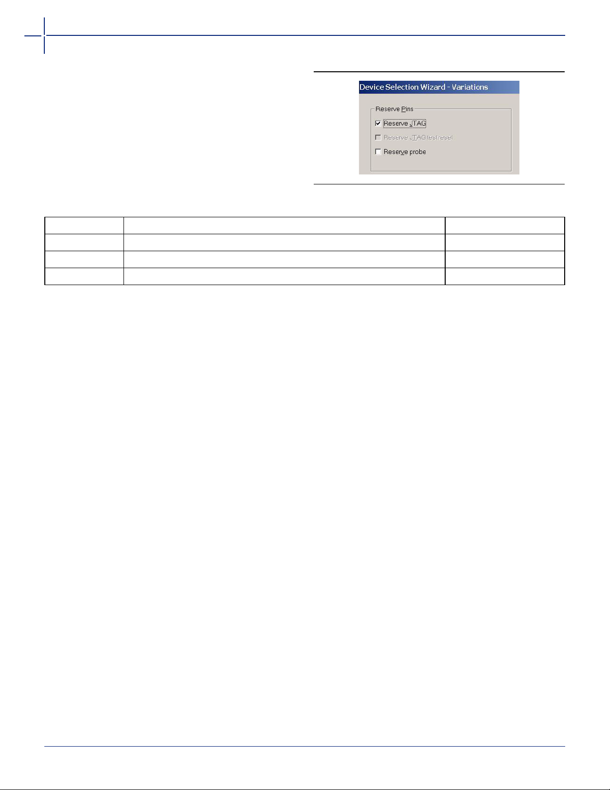
The JTAG test logic circuit is activated in the Designer
software by selecting Tools -> Device Selection. This
brings up the Device Selection dialog box as shown in
Figure 1-15. The JTAG test logic circuit can be enabled by
clicking the "Reserve JTAG Pins" check box. Table 5
explains the pins' behavior in either mode.
Figure 1-15 • Device Selection Wizard
Tabl e 5 • Boundary Scan Pin Configuration and Functionality
Reserve JTAG Checked Unchecked
TCK BST input; must be terminated to logical HIGH or LOW to avoid floating User I/O
TDI, TMS BST input; may float or be tied to HIGH User I/O
TDO BST output; may float or be connected to TDI of another device User I/O
TRST Pin and TAP Controller Reset
An active reset (TRST) pin is not supported; however, MX
devices contain power-on circuitry that resets the
boundary scan circuitry upon power-up. Also, the TMS
pin is equipped with an internal pull-up resistor. This
allows the TAP controller to remain in or return to the
Test-Logic-Reset state when there is no input or when a
logical 1 is on the TMS pin. To reset the controller, TMS
must be HIGH for at least five TCK cycles.
Boundary Scan Description Language (BSDL) File
Conforming to the IEEE Standard 1149.1 requires that
the operation of the various JTAG components be
documented. The BSDL file provides the standard format
to describe the JTAG components that can be used by
automatic test equipment software. The file includes the
instructions that are supported, instruction bit pattern,
and the boundary-scan chain order. For an in-depth
discussion on BSDL files, please refer to Actel BSDL Files
Format Description application note.
Actel BSDL files are grouped into two categories generic and device-specific. The generic files assign all
user I/Os as inouts. Device-specific files assign user I/Os as
inputs, outputs or inouts.
Generic files for MX devices are available on Actel's website
at http://www.actel.com/techdocs/models/bsdl.html.
1-12 v6.0
Page 19

40MX and 42MX FPGA Families
Development Tool Support
The MX family of FPGAs is fully supported by both Actel's
Libero™ Integrated Design Environment and Designer
FPGA Development software. Actel Libero IDE is a design
management environment that streamlines the design
flow. Libero IDE provides an integrated design manager
that seamlessly integrates design tools while guiding the
user through the design flow, managing all design and
log files, and passing necessary design data among tools.
Additionally, Libero IDE allows users to integrate both
schematic and HDL synthesis into a single flow and verify
the entire design in a single environment. Libero IDE
includes Synplify® for Actel from Synplicity®, ViewDraw
for Actel from Mentor Graphics, ModelSim™ HDL
Simulator from Mentor Graphics®, WaveFormer Lite™
from SynaptiCAD™, and Designer software from Actel.
Refer to the Libero IDE flow (located on Actel’s website)
diagram for more information.
Actel's Designer software is a place-and-route tool and
provides a comprehensive suite of backend support tools
for FPGA development. The Designer software includes
timing-driven place-and-route, and a world-class
integrated static timing analyzer and constraints editor.
With the Designer software, a user can lock his/her
design pins before layout while minimally impacting the
results of place-and-route. Additionally, the backannotation flow is compatible with all the major
simulators and the simulation results can be cross-probed
with Silicon Explorer II, Actel’s integrated verification
and logic analysis tool. Another tool included in the
Designer software is the ACTgen macro builder, which
easily creates popular and commonly used logic
functions for implementation into your schematic or HDL
design. Actel's Designer software is compatible with the
most popular FPGA design entry and verification tools
from companies such as Mentor Graphics, Synplicity,
Synopsys, and Cadence Design Systems. The Designer
software is available for both the Windows and UNIX
operating systems.
Actel's Designer software is compatible with the most
popular FPGA design entry and verification tools from
companies such as Mentor Graphics, Synplicity, Synopsys,
and Cadence Design Systems. The Designer software is
available for both the Windows and UNIX operating
systems.
Related Documents
Application Notes
Actel BSDL Files Format Description
www.actel.com/documents/BSDLformat_AN.pdf
Programming Antifuse Devices
http://www.actel.com/documents/
AntifuseProgram_AN.pdf
Actel's Implementation of Security in Actel Antifuse
FPGAs
www.actel.com/documents/Antifuse_Security_AN.pdf
User’s Guides and Manuals
Antifuse Macro Library Guide
www.actel.com/documents/libguide_UG.pdf
Silicon Sculptor II
www.actel.com/techdocs/manuals/default.asp#programmers
Miscellaneous
Libero IDE Flow Diagram
www.actel.com/products/tools/libero/flow.html
v6.0 1-13
Page 20
40MX and 42MX FPGA Families
5.0V Operating Conditions
Tabl e 6 • Absolute Maximum Ratings for 40MX Devices*
Symbol Parameter Limits Units
V
V
V
t
CC
I
O
STG
DC Supply Voltage –0.5 to +7.0 V
Input Voltage –0.5 to VCC+0.5 V
Output Voltage –0.5 to VCC+0.5 V
Storage Temperature –65 to +150 °C
Note: *Stresses beyond those listed under "Absolute Maximum Ratings" may cause permanent damage to the device. Exposure to
absolute maximum rated conditions for extended periods may affect device reliability. Devices should not be operated outside the
Recommended Operating Conditions.
Tabl e 7 • Absolute Maximum Ratings for 42MX Devices*
Symbol Parameter Limits Units
V
V
V
V
t
CCI
CCA
I
O
STG
DC Supply Voltage for I/Os –0.5 to +7.0 V
DC Supply Voltage for Array –0.5 to +7.0 V
Input Voltage –0.5 to V
Output Voltage –0.5 to V
+0.5 V
CCI
+0.5 V
CCI
Storage Temperature –65 to +150 °C
Note: *Stresses beyond those listed under "Absolute Maximum Ratings" may cause permanent damage to the device. Exposure to
absolute maximum rated conditions for extended periods may affect device reliability. Devices should not be operated outside the
Recommended Operating Conditions.
Tabl e 8 • Recommended Operating Conditions
Parameter Commercial Industrial Military Units
Temperature Range* 0 to +70 -40 to +85 –55 to +125 °C
(40MX) 4.75 to 5.25 4.5 to 5.5 4.5 to 5.5 V
V
CC
(42MX) 4.75 to 5.25 4.5 to 5.5 4.5 to 5.5 V
V
CCA
V
(42MX) 4.75 to 5.25 4.5 to 5.5 4.5 to 5.5 V
CCI
Note: *Ambient temperature (T
) is used for commercial and industrial grades; case temperature (TC) is used for military grades.
A
1-14 v6.0
Page 21
5V TTL Electrical Specifications
Tabl e 9 • 5V TTL Electrical Specifications
Commercial Commercial -F Industrial Military
40MX and 42MX FPGA Families
Symbol Parameter
1
V
OH
1
V
OL
V
IL
(40MX) 2.0 VCC+0.3 2.0 VCC+0.3 2.0 VCC+0.3 2.0 VCC+0.3 V
V
IH
(42MX) 2.0 V
V
IH
I
IL
I
IH
Input Transition
Time, T
C
Standby Current,
I
CC
and T
R
F
I/O Capacitance 10101010pF
IO
2
IOH = -10mA 2.4 2.4 V
I
= -4mA 3.7 3.7 V
OH
IOL = 10mA 0.5 0.5 V
= 6mA 0.4 0.4 V
I
OL
-0.3 0.8 -0.3 0.8 -0.3 0.8 -0.3 0.8 V
+0.3 2.0 V
CCI
+0.3 2.0 V
CCI
+0.3 2.0 V
CCI
CCI
VIN = 0.5V -10 -10 -10 -10 µA
VIN = 2.7V -10 -10 -10 -10 µA
500 500 500 500 ns
A40MX02,
3 251025mA
A40MX04
UnitsMin. Max. Min. Max. Min. Max. Min. Max.
+0.3 V
A42MX09 5 25 25 25 mA
A42MX16 6 25 25 25 mA
A42MX24,
20 25 25 25 mA
A42MX36
Low-Power Mode
Standby Current
I
I/O source sink
IO,
42MX devices
0.5 ICC - 5.0 ICC - 5.0 ICC - 5.0 mA
only
Can be derived from the IBIS model (http://www.actel.com/techdocs/models/ibis.html)
current
Notes:
1. Only one output tested at a time. V
2. All outputs unloaded. All inputs = V
CC/VCCI
CC/VCCI
= min.
or GND.
v6.0 1-15
Page 22
40MX and 42MX FPGA Families
3.3V Operating Conditions
Table 10 • Absolute Maximum Ratings for 40MX Devices*
Symbol Parameter Limits Units
V
V
V
t
CC
I
O
STG
DC Supply Voltage –0.5 to +7.0 V
Input Voltage –0.5 to VCC+0.5 V
Output Voltage –0.5 to VCC+0.5 V
Storage Temperature –65 to +150 °C
Note: *Stresses beyond those listed under "Absolute Maximum Ratings" may cause permanent damage to the device. Exposure to
absolute maximum rated conditions for extended periods may affect device reliability. Devices should not be operated outside the
Recommended Operating Conditions.
Table 11 • Absolute Maximum Ratings for 42MX Devices*
Symbol Parameter Limits Units
V
V
V
V
t
CCI
CCA
I
O
STG
DC Supply Voltage for I/Os –0.5 to +7.0 V
DC Supply Voltage for Array –0.5 to +7.0 V
Input Voltage –0.5 to V
Output Voltage –0.5 to V
+0.5 V
CCI
+0.5 V
CCI
Storage Temperature –65 to +150 °C
Note: *Stresses beyond those listed under "Absolute Maximum Ratings" may cause permanent damage to the device. Exposure to
absolute maximum rated conditions for extended periods may affect device reliability. Devices should not be operated outside the
Recommended Operating Conditions.
Table 12 • Recommended Operating Conditions
Parameter Commercial Industrial Military Units
Temperature Range* 0 to +70 –40 to +85 –55 to +125 °C
(40MX) 3.0 to 3.6 3.0 to 3.6 3.0 to 3.6 V
V
CC
(42MX) 3.0 to 3.6 3.0 to 3.6 3.0 to 3.6 V
V
CCA
V
(42MX) 3.0 to 3.6 3.0 to 3.6 3.0 to 3.6 V
CCI
Note: *Ambient temperature (T
) is used for commercial and industrial grades; case temperature (TC) is used for military grades.
A
1-16 v6.0
Page 23
3.3V LVTTL Electrical Specifications
Table 13 • 3.3V LVTTL Electrical Specifications
Commercial Commercial -F Industrial Military
40MX and 42MX FPGA Families
Symbol Parameter
1
V
OH
1
V
OL
V
IL
(40MX) 2.0 VCC+0.3 2.0 VCC+0.3 2.0 VCC+0.3 2.0 VCC+0.3 V
V
IH
V
(42MX) 2.0 V
IH
I
IL
I
IH
Input Transition Time,
T
and T
R
F
I/O Capacitance 10 10 10 10 pF
C
IO
Standby Current, I
CC
I
= –4mA 2.15 2.15 2.4 2.4 V
OH
IOL = 6mA 0.4 0.4 0.48 0.48 V
–0.3 0.8 –0.3 0.8 –0.3 0.8 –0.3 0.8 V
+0.3 2.0 V
CCI
+0.3 2.0 V
CCI
+0.3 2.0 V
CCI
CCI
–10 –10 –10 –10 µA
–10 –10 –10 –10 µA
500 500 500 500 ns
2
A40MX02,
3251025mA
+0.3 V
A40MX04
A42MX09 5 25 25 25 mA
A42MX16 6 25 25 25 mA
A42MX24,
15 25 25 25 mA
A42MX36
Low-Power Mode
Standby Current
I/O source sink
I
IO,
42MX
0.5 ICC - 5.0 ICC - 5.0 ICC - 5.0 mA
devices only
Can be derived from the IBIS model (http://www.actel.com/techdocs/models/ibis.html)
current
Notes:
1. Only one output tested at a time. V
2. All outputs unloaded. All inputs = V
CC/VCCI
CC/VCCI
= min.
or GND.
UnitsMin. Max. Min. Max. Min. Max. Min. Max.
v6.0 1-17
Page 24
40MX and 42MX FPGA Families
Mixed 5.0V/3.3V Operating Conditions (for 42MX Devices Only)
Table 14 • Absolute Maximum Ratings*
Symbol Parameter Limits Units
V
CCI
V
CCA
V
I
V
O
t
STG
Note: *Stresses beyond those listed under "Absolute Maximum Ratings" may cause permanent damage to the device. Exposure to
absolute maximum rated conditions for extended periods may affect device reliability. Devices should not be operated outside the
Recommended Operating Conditions.
Table 15 • Recommended Operating Conditions
Parameter Commercial Industrial Military Units
Temperature Range* 0 to +70 -40 to +85 –55 to +125 °C
V
4.75 to 5.25 4.5 to 5.5 4.5 to 5.5 V
CCA
V
3.14 to 3.47 3.0 to 3.6 3.0 to 3.6 V
CCI
Note: *Ambient temperature (T
DC Supply Voltage for I/Os –0.5 to +7.0 V
DC Supply Voltage for Array –0.5 to +7.0 V
Input Voltage –0.5 to V
Output Voltage –0.5 to V
+0.5 V
CCI
+0.5 V
CCI
Storage Temperature –65 to +150 °C
) is used for commercial and industrial grades; case temperature (TC) is used for military grades.
A
Mixed 5.0V/3.3V Electrical Specifications
Table 16 • Mixed 5.0V/3.3V Electrical Specifications
Commercial Commercial '-F 'Industrial Military
Symbol Parameter
1
V
OH
1
V
OL
IOH = –10mA 2.4 2.4 V
I
= –4mA 3.7 3.7 V
OH
IOL = 10mA 0.5 0.5 V
IOL = 6mA 0.4 0.4 V
V
IL
V
IH
I
L
I
H
Input Transition Time, T
I/O Capacitance 10 10 10 10 pF
C
IO
Standby Current, I
CC
2
and T
R
F
VIN = 0.5V –10 –10 –10 –10 µA
VIN = 2.7V –10 –10 –10 –10 µA
A42MX09 5 25 25 25 mA
–0.3 0.8 –0.3 0.8 –0.3 0.8 –0.3 0.8 V
2.0 V
+0.3 2.0 V
CCI
+0.3 2.0 V
CCI
+0.3 2.0 V
CCI
CCI
500 500 500 500 ns
A42MX16 6 25 25 25 mA
A42MX24, A42MX36 20 25 25 25 mA
Low-Power Mode Standby Current 0.5 ICC - 5.0 ICC - 5.0 ICC - 5.0 mA
I
I/O source sink current Can be derived from the IBIS model (http://www.actel.com/techdocs/models/ibis.html)
IO
Notes:
1. Only one output tested at a time. V
2. All outputs unloaded. All inputs = V
= min.
CCI
or GND.
CCI
UnitsMin. Max. Min. Max. Min. Max. Min. Max.
+0.3 V
1-18 v6.0
Page 25
40MX and 42MX FPGA Families
Output Drive Characteristics for 5.0V PCI Signaling
MX PCI device I/O drivers were designed specifically for high-performance PCI systems. Figure 1-16 on page 1-21 shows
the typical output drive characteristics of the MX devices. MX output drivers are compliant with the PCI Local Bus
Specification.
OUT
I
OUT
OUT
1
= –2 mA
= –6 mA
= 3 mA,
6 mA
PCI MX
2.4
0.55 — 0.33 V
3.84
2
+ 0.3 V
CCI
3
V
V
nH
Table 17 • DC Specification (5.0V PCI Signaling)
Symbol Parameter Condition Min. Max. Min. Max. Units
V
CCI
V
IH
V
IL
I
IH
I
IL
V
OH
V
OL
C
IN
C
CLK
L
PIN
Supply Voltage for I/Os 4.75 5.25 4.75 5.25
Input High Voltage 2.0 VCC + 0.5 2.0 V
Input Low Voltage –0.5 0.8 –0.3 0.8 V
Input High Leakage Current VIN = 2.7V 70 — 10 µA
Input Low Leakage Current VIN=0.5V –70 — –10 µA
Output High Voltage I
Output Low Voltage I
Input Pin Capacitance 10 — 10 pF
CLK Pin Capacitance 5 12 — 10 pF
Pin Inductance 20 — < 8 nH
Notes:
1. PCI Local Bus Specification, Version 2.1, Section 4.2.1.1.
2. Maximum rating for V
–0.5V to 7.0V.
CCI
3. Dependent upon the chosen package. PCI recommends QFP and BGA packaging to reduce pin inductance and capacitance.
Table 18 • AC Specifications (5.0V PCI Signaling)*
PCI MX
Symbol Parameter Condition Min. Max. Min. Max. Units
I
CL
Low Clamp Current –5 < VIN ≤ –1 –25 + (VIN +1)
–60 –10 mA
/0.015
Slew (r) Output Rise Slew Rate 0.4V to 2.4V load 1 5 1.8 2.8 V/ns
Slew (f) Output Fall Slew Rate 2.4V to 0.4V load 1 5 2.8 4.3 V/ns
Note: *PCI Local Bus Specification, Version 2.1, Section 4.2.1.2.
v6.0 1-19
Page 26
40MX and 42MX FPGA Families
Output Drive Characteristics for 3.3V PCI Signaling
Table 19 • DC Specification (3.3V PCI Signaling)
Symbol Parameter Condition Min. Max. Min. Max. Units
V
CCI
V
IH
V
IL
I
IH
I
IL
V
OH
V
OL
C
IN
C
CLK
L
PIN
Supply Voltage for I/Os 3.0 3.6 3.0 3.6 V
Input High Voltage 0.5 VCC + 0.5 0.5 V
Input Low Voltage –0.5 0.8 –0.3 0.8 V
Input High Leakage Current VIN = 2.7V 70 10 µA
Input Leakage Current –70 –10 µA
Output High Voltage I
Output Low Voltage I
Input Pin Capacitance 10 10 pF
CLK Pin Capacitance 5 12 10 pF
Pin Inductance 20 < 8 nH
Notes:
1. PCI Local Bus Specification, Version 2.1, Section 4.2.2.1.
2. Maximum rating for V
–0.5V to 7.0V.
CCI
3. Dependent upon the chosen package. PCI recommends QFP and BGA packaging to reduce pin inductance and capacitance.
1
PCI MX
+ 0.3 V
CCI
= –2 mA 0.9 3.3 V
OUT
= 3 mA,
OUT
0.1 0.1 V
CCI
6 mA
3
V
nH
Table 20 • AC Specifications for (3.3V PCI Signaling)*
PCI MX
Symbol Parameter Condition Min. Max. Min. Max. Units
I
CL
Low Clamp Current –5 < VIN ≤ –1 –25 + (VIN +1)
–60 –10 mA
/0.015
Slew (r) Output Rise Slew Rate 0.2V to 0.6V load 1 4 1.8 2.8 V/ns
Slew (f) Output Fall Slew Rate 0.6V to 0.2V load 1 4 2.8 4.0 V/ns
Note: *PCI Local Bus Specification, Version 2.1, Section 4.2.2.2.
1-20 v6.0
Page 27
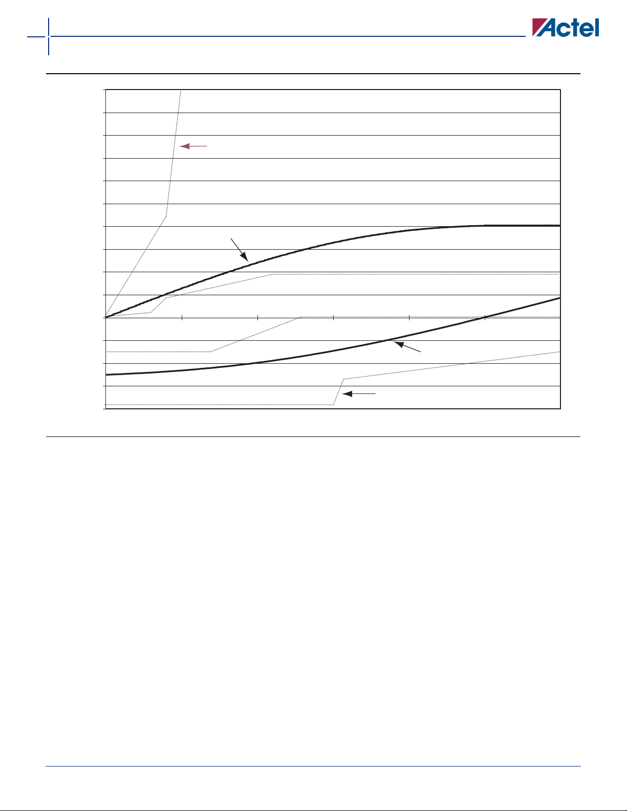
0.50
0.45
40MX and 42MX FPGA Families
0.40
0.35
0.30
0.25
0.20
0.15
0.10
Current (A)
0.05
0.00
01 2 3 4 5 6
–0.05
–0.10
–0.15
–0.20
PCI I
Maximum
OH
PCI IOL Maximum
MX PCI I
OL
Voltage Out (V)
PCI I
PCI I
MX PCI I
Minimum
OH
Minimum
OL
OH
Figure 1-16 • Typical Output Drive Characteristics (Based Upon Measured Data)
v6.0 1-21
Page 28
40MX and 42MX FPGA Families
Junction Temperature (TJ)
The temperature variable in the Designer software refers
to the junction temperature, not the ambient
temperature. This is an important distinction because the
P = Power
θ
= Junction to ambient of package. θja numbers are
ja
located in the Package Thermal Characteristics table
below.
heat generated from dynamic power consumption is
usually hotter than the ambient temperature. EQ 1-1,
shown below, can be used to calculate junction
temperature.
EQ 1-1
Junction Temperature = ∆T + T
a
(1)
Where:
T
= Ambient Temperature
a
∆T = Temperature gradient between junction (silicon)
and ambient
θ
∆T =
* P(2)
ja
Maximum Power Allowed
Max. junction temp. (° C) Max. ambient temp. (°C)–
---------------------------------------------------------------------------------------------------------------------------------
θ
The maximum power dissipation for military-grade devices is a function of
Package Thermal Characteristics
The device junction-to-case thermal characteristic is θjc,
and the junction-to-ambient air characteristic is θ
thermal characteristics for θ
different air flow rates.
The maximum junction temperature is 150°C.
Maximum power dissipation for commercial- and
industrial-grade devices is a function of
A sample calculation of the absolute maximum power
dissipation allowed for a TQFP 176-pin package at
commercial temperature and still air is as follow:
150° C70°C–
(° C/W)
ja
---------------------------------- 28° C/W
θ
. A sample calculation of the absolute
jc
are shown with two
ja
θ
ja
2.86W===
.
maximum power dissipation allowed for CQFP 208-pin package at military temperature and still air is as follows:
Maximum Power Allowed
Max. junction temp. (°C) Max. ambient temp. (° C)–
---------------------------------------------------------------------------------------------------------------------------------
θ
jc
(° C/W)
150° C 125°C–
------------------------------------- -
6.3°C/W
3.97W===
. The
ja
Table 21 • Package Thermal Characteristics
θ
ja
1.0 m/s
Plastic Packages Pin Count
Plastic Quad Flat Pack 100 12.0 27.8 23.4 21.2 °C/W
Plastic Quad Flat Pack 160 10.0 26.2 22.8 21.1 °C/W
Plastic Quad Flat Pack 208 8.0 26.1 22.5 20.8 °C/W
Plastic Quad Flat Pack 240 8.5 25.6 22.3 20.8 °C/W
Plastic Leaded Chip Carrier 44 16.0 20.0 24.5 22.0 °C/W
Plastic Leaded Chip Carrier 68 13.0 25.0 21.0 19.4 °C/W
Plastic Leaded Chip Carrier 84 12.0 22.5 18.9 17.6 °C/W
Thin Plastic Quad Flat Pack 176 11.0 24.7 19.9 18.0 °C/W
Very Thin Plastic Quad Flat Pack 80 12.0 38.2 31.9 29.4 °C/W
Very Thin Plastic Quad Flat Pack 100 10.0 35.3 29.4 27.1 °C/W
Plastic Ball Grid Array 272 3.0 18.3 14.9 13.9 °C/W
Ceramic Packages
Ceramic Quad Flat Pack 208 2.0 22.0 19.8 18.0 °C/W
θ
jc
200 ft/min.
2.5 m/s
500 ft/min.
UnitsStill Air
Ceramic Quad Flat Pack 256 2.0 20.0 16.5 15.0 °C/W
1-22 v6.0
Page 29
Timing Models
40MX and 42MX FPGA Families
I/O Module
t
INYL=0.62 ns
t
IRD2=2.59 ns
t
IRD1=2.09 ns
t
IRD4=3.64 ns
t
IRD8=5.73 ns
Internal Delays
Logic Module
t
PD=1.24 ns
t
CO=1.24 ns
Predicted
Routing
Delays
t
RD1=1.28 ns
t
RD2=1.80 ns
t
RD4=2.33 ns
t
RD8=4.93 ns
Output DelayInput Delay
I/O Module
t
t
ENHZ=7.92 ns
DLH=3.32 ns
Array
Clock
t
CKH=4.55 ns
F
MAX=180 MHz
FO=128
Note: * Values are shown for 40MX ‘–3’ speed devices at 5.0V worst-case commercial conditions.
Figure 1-17 • 40MX Timing Model*
Output DelaysInternal DelaysInput Delays
I/O Module
I/O Module
DQ
G
t
OUTH=0.00 ns
t
OUTSU=0.3 ns
t
GLH=2.6 ns
t
Array
Clocks
I/O Module
t
INH=0.0 ns
t
INSU=0.3 ns
t
INGL=1.3 ns
t
CKH=2.70 ns
F
MAX=296 MHz
t
INYL=0.8 ns
DQ
G
FO = 32
t
IRD1=2.0 ns
Predicted
Routi ng
t
t
t
t
DQ
t
CO=1.3 ns
Delays
RD1=0.7 ns
RD2=1.9 ns
RD4=1.4 ns
RD8=2.3 ns
†
Combinatorial
Logic M odule
t
PD=1.2 ns
Sequential
Logic M odule
Combin
at or ia l
-
Logic
incl ude
t
SUD=0.3 ns
t
HD=0.00 ns
t
LCO=5.2 ns (light loads, pad-to-pad)
t
RD1=0.70 ns
DLH=2.5 ns
t
DLH=2.5 ns
t
ENHZ=4.9 ns
Notes: *Values are shown for A42MX09 ‘–3’ at 5.0V worst-case commercial conditions.
† Input module predicted routing delay.
Figure 1-18 • 42MX Timing Model*
v6.0 1-23
Page 30
40MX and 42MX FPGA Families
Predicted
Routi ng
t
t
t
t
DQ
t
CO=1.3 ns
Delays
RD1=0.7 ns
RD2=1.9 ns
RD4=1.4 ns
RD8=2.3 ns
t
RD1=0.70 ns
Array
Clocks
I/O Module
t
INH=0.0 ns
t
INSU=0.3 ns
t
INGL=1.3 ns
t
CKH=2.70 ns
F
MAX=296 MHz
t
INYL=0.8 ns
DQ
G
FO = 32
t
IRD1=2.0 ns
†
Combinatorial
Logic M odule
t
PD=1.2 ns
Sequential
Logic M odule
Combin
at or ia l
-
Logic
incl ude
t
SUD=0.3 ns
t
HD=0.00 ns
t
LCO=5.2 ns (light loads, pad-to-pad)
Notes: * Values are shown for A42MX36 ‘–3’ at 5.0V worst-case commercial conditions.
** Load-dependent
Figure 1-19 • 42MX Timing Model (Logic Functions Using Quadrant Clocks)
Input Delays
Output DelaysInternal DelaysInput Delays
I/O Module
I/O Module
DQ
G
t
OUTH=0.00 ns
t
OUTSU=0.3 ns
t
GLH=2.6 ns
t
DLH=2.5 ns
t
DLH=2.5 ns
t
ENHZ=4.9 ns
I/O Module
t
INPY=1.0ns
t
IRD1=2.0ns
DQ
G
t
INSU=0.5ns
t
INH=0.0ns
t
INGO=1.4ns
WD [7:0]
WRAD [5:0]
BLKEN
RD [7:0]
R DAD [5 :0]
REN
Predicte d
Routing
Delays
t
RD1=0.9ns
WEN
Array
Clocks
F
MAX
=167 MHz
WCLK
t
ADSU=1.6ns
t
ADH=0.0ns
t
WENSU=2.7ns
t
BENS=2.8ns
RCLK
t
ADSU=1.6ns
t
ADH=0.0ns
t
RENSU=0.6ns
t
RCO=3.4ns
Note: *Values are shown for A42MX36 ‘–3 at 5.0V worst-case commercial conditions.
Figure 1-20 • 42MX Timing Model (SRAM Functions)
I/O Module
t
DLH=2.6ns
DQ
G
t
GHL=2.9ns
t
LSU=0.5ns
t
LH=0.0ns
1-24 v6.0
Page 31

Parameter Measurement
D
TRIBUFF
40MX and 42MX FPGA Families
E
To AC test loads (shown below)
PAD
In
50%
50%
V
t
DLH
OH
1.5V
PA D
V
OL
Figure 1-21 • Output Buffer Delays
(Used to measure propagation delay)
To the output under test
Figure 1-22 • AC Test Loads
PA D
IN BUF
t
DHL
Load 1
Y
1.5V
35 pF
E
PA D
50%
50%
V
CCI
1.5V
V
OL
t
ENZL
t
ENLZ
To the output under test
E
V
PA D
GND
Load 2
CCI
10%
(Used to measure rising/falling edges)
50%
50%
V
OH
1.5V
t
ENZH
GND
R to V
for tPLZ/tPZL
CCI
R to GND for tPHZ/tPZH
R=1k
Ω
35 pF
t
ENHZ
90%
S
A
B
Y
1.5V
t
INYH
3V
1.5V
V
50%
CCI
PA D
Y
GND
Figure 1-23 • Input Buffer Delays
t
INYL
0V
50%
S, A or B
50%
50%
PHL
t
PLH
50%
50%
Y
Y
t
PLH
50%
t
PHL
50%
Figure 1-24 • Module Delays
v6.0 1-25
Page 32

40MX and 42MX FPGA Families
Sequential Module Timing Characteristics
PRE Y
D
E
G, CLK
PRE, CLR
D*
E
Q
t
CLK
(Positive Edge-T riggered)
SUD
t
WCLKA
t
SU EN A
CLR
t
HD
t
HENA
t
CO
t
WCLKI
t
WASYN
t
A
t
RS
Note: *D represents all data functions involving A, B, and S for multiplexed flip-flops.
Figure 1-25 • Flip-Flops and Latches
1-26 v6.0
Page 33

Sequential Timing Characteristics
40MX and 42MX FPGA Families
CLK
Figure 1-26 • Input Buffer Latches
PA D
DATA
CLK
DATA
G
PA D
G
t
INSU
t
SU EX T
D
IBDL
PAD
t
HEXT
t
INH
OBDLHS
G
Figure 1-27 • Output Buffer Latches
D
t
OUTSU
G
t
OUTH
v6.0 1-27
Page 34

40MX and 42MX FPGA Families
Decode Module Timing
A
B
C
D
E
F
G
H
Y
A–G, H
50%
Y
t
PLH
Figure 1-28 • Decode Module Timing
SRAM Timing Characteristics
Write Port
WRAD [5:0]
BLKEN
WEN
WCLK
WD [7:0 ]
Figure 1-29 • SRAM Timing Characteristics
RAM Array
32x8 or 64x 4
(256 Bits)
t
PHL
Read Port
RDAD [5:0]
LEW
REN
RCLK
RD [7:0]
Dual-Port SRAM Timing Waveforms
WCLK
t
WD[7:0]
WRAD[5:0]
WEN
BLKEN
Note: Identical timing for falling edge clock.
Figure 1-30 • 42MX SRAM Write Operation
1-28 v6.0
ADSU
Valid
t
WENSU
t
BENSU
Valid
t
RCKHL
t
t
t
ADH
WENH
BENH
t
RCKHL
Page 35

40MX and 42MX FPGA Families
t
CKHL
RCLK
REN
RDAD[5:0]
RD[7:0]
Note: Identical timing for falling edge clock.
Figure 1-31 • 42MX SRAM Synchronous Read Operation
RDAD[5:0]
t
RDADV
t
Old Data
t
DOH
RCKHL
t
RENSU
t
ADSU
Valid
t
DOH
t
RENH
t
ADH
t
RCO
New Data
ADDR2ADDR1
t
RPD
RD[7:0]
Data 1
Data 2
Figure 1-32 • 42MX SRAM Asynchronous Read Operation—Type 1 (Read Address Controlled)
WEN
t
WENSU
t
WENH
WD[7:0]
WRAD[5:0]
Valid
BLKEN
t
DOH
t
ADH
t
RPD
New Data
WCLK
RD[7:0]
t
ADSU
Old Data
Figure 1-33 • 42MX SRAM Asynchronous Read Operation—Type 2 (Write Address Controlled)
v6.0 1-29
Page 36

40MX and 42MX FPGA Families
Predictable Performance: Tight Delay Distributions
Propagation delay between logic modules depends on
the resistive and capacitive loading of the routing tracks,
the interconnect elements, and the module inputs being
driven. Propagation delay increases as the length of
routing tracks, the number of interconnect elements, or
the number of inputs increases.
From a design perspective, the propagation delay can be
statistically correlated or modeled by the fanout
(number of loads) driven by a module. Higher fanout
usually requires some paths to have longer routing
tracks.
The MX FPGAs deliver a tight fanout delay distribution,
which is achieved in two ways: by decreasing the delay of
the interconnect elements and by decreasing the number
of interconnect elements per path.
Actel’s patented antifuse offers a very low resistive/
capacitive interconnect. The antifuses, fabricated in
0.45 µm lithography, offer nominal levels of 100Ω
resistance and 7.0fF capacitance per antifuse.
MX fanout distribution is also tight due to the low
number of antifuses required for each interconnect path.
The proprietary architecture limits the number of
antifuses per path to a maximum of four, with
90 percent of interconnects using only two antifuses.
Timing Characteristics
Device timing characteristics fall into three categories:
family-dependent, device-dependent, and designdependent. The input and output buffer characteristics
are common to all MX devices. Internal routing delays
are device-dependent; actual delays are not determined
until after place-and-route of the user's design is
complete. Delay values may then be determined by using
the Designer software utility or by performing
simulation with post-layout delays.
Critical Nets and Typical Nets
Propagation delays are expressed only for typical nets,
which are used for initial design performance evaluation.
Critical net delays can then be applied to the most timing
critical paths. Critical nets are determined by net
property assignment in Actel's Designer software prior to
placement and routing. Up to 6% of the nets in a design
may be designated as critical.
Long Tracks
Some nets in the design use long tracks, which are
special routing resources that span multiple rows,
columns, or modules. Long tracks employ three and
sometimes four antifuse connections, which increase
capacitance and resistance, resulting in longer net delays
for macros connected to long tracks. Typically, up to
6 percent of nets in a fully utilized device require long
tracks. Long tracks add approximately a 3 ns to a 6 ns
delay, which is represented statistically in higher fanout
(FO=8) routing delays in the data sheet specifications
section, shown in Table 28 on page 1-36.
Timing Derating
MX devices are manufactured with a CMOS process.
Therefore, device performance varies according to
temperature, voltage, and process changes. Minimum
timing parameters reflect maximum operating voltage,
minimum operating temperature and best-case
processing. Maximum timing parameters reflect
minimum operating voltage, maximum operating
temperature and worst-case processing.
1-30 v6.0
Page 37

40MX and 42MX FPGA Families
Temperature and Voltage Derating Factors
Table 22 • 42MX Temperature and Voltage Derating Factors
(Normalized to T
42MX Voltage
= 25°C, V
J
–55°C –40°C 0°C 25°C 70°C 85°C 125°C
4.50 0.93 0.95 1.05 1.09 1.25 1.29 1.41
4.75 0.88 0.90 1.00 1.03 1.18 1.22 1.34
5.00 0.85 0.87 0.96 1.00 1.15 1.18 1.29
5.25 0.84 0.86 0.95 0.97 1.12 1.14 1.28
5.50 0.83 0.85 0.94 0.96 1.10 1.13 1.26
1.50
1.40
CCA
= 5.0V)
Temperature
1.30
1.20
1.10
1.00
0.90
Derating Factor
0.80
0.70
0.60
4.50 4.75 5.00 5.25 5.50
Voltage (V)
Note: This derating factor applies to all routing and propagation delays.
Figure 1-34 • 42MX Junction Temperature and Voltage Derating Curves
(Normalized to T
= 25°C, V
J
CCA
= 5.0V)
–55˚C
–40˚C
0˚C
25˚C
70˚C
85˚C
125˚C
v6.0 1-31
Page 38

40MX and 42MX FPGA Families
Table 23 • 40MX Temperature and Voltage Derating Factors
(Normalized to TJ = 25°C, VCC = 5.0V)
Temperature
40MX Voltage
–55°C –40°C 0°C 25°C 70°C 85°C 125°C
4.50 0.89 0.93 1.02 1.09 1.25 1.31 1.45
4.75 0.84 0.88 0.97 1.03 1.18 1.24 1.37
5.00 0.82 0.85 0.94 1.00 1.15 1.20 1.33
5.25 0.80 0.82 0.91 0.97 1.12 1.16 1.29
5.50 0.79 0.82 0.90 0.96 1.10 1.15 1.28
1.50
1.40
1.30
1.20
Factor
1.10
1.00
0.90
Derating
0.80
0.70
0.60
4.50 4.75 5.00 5.25 5.50
–55˚C
–40˚C
0˚C
25˚C
70˚C
85˚C
125˚C
Voltage (V)
Note: This derating factor applies to all routing and propagation delays.
Figure 1-35 • 40MX Junction Temperature and Voltage Derating Curves
(Normalized to T
= 25°C, VCC = 5.0V)
J
1-32 v6.0
Page 39

40MX and 42MX FPGA Families
Table 24 • 42MX Temperature and Voltage Derating Factors
(Normalized to TJ = 25°C, V
CCA
= 3.3V)
Temperature
42MX Voltage
–55°C –40°C 0°C 25°C 70°C 85°C 125°C
3.00 0.97 1.00 1.10 1.15 1.32 1.36 1.45
3.30 0.84 0.87 0.96 1.00 1.15 1.18 1.26
3.60 0.81 0.84 0.92 0.96 1.10 1.13 1.21
1.60
1.50
1.40
55˚C
40˚C
0˚C
25˚C
70˚C
85˚C
125˚C
Derating Factor
1.30
1.20
1.10
1.00
0.90
0.80
0.70
0.60
0.50
0.40
3.00 3.30 3.60
Voltage (V)
(V)
Note: This derating factor applies to all routing and propagation delays.
Figure 1-36 • 42MX Junction Temperature and Voltage Derating Curves
(Normalized to T
= 25°C, V
J
CCA
= 3.3V)
v6.0 1-33
Page 40

40MX and 42MX FPGA Families
Table 25 • 40MX Temperature and Voltage Derating Factors
(Normalized to TJ = 25°C, VCC = 3.3V)
Temperature
40MX Voltage
3.00 1.08 1.12 1.21 1.26 1.50 1.64 2.00
3.30 0.86 0.89 0.96 1.00 1.19 1.30 1.59
3.60 0.83 0.85 0.92 0.96 1.14 1.25 1.53
2.20
2.00
–55°C –40°C 0°C 25°C 70°C 85°C 125°C
55˚C
1.80
1.60
1.40
40˚C
0˚C
25˚C
70˚C
1.20
Derating Factor
1.00
85˚C
125˚C
0.80
0.60
3.00 3.30 3.60
Voltage (V)
Note: This derating factor applies to all routing and propagation delays.
Figure 1-37 • 40MX Junction Temperature and Voltage Derating Curves
(Normalized to TJ = 25°C, VCC = 3.3V)
1-34 v6.0
Page 41

40MX and 42MX FPGA Families
PCI System Timing Specification
Table 26 and Table 27 list the critical PCI timing
parameters and the corresponding timing parameters
for the MX PCI-compliant devices.
PCI Models
Actel provides synthesizable VHDL and Verilog-HDL
models for a PCI Target interface, a PCI Target and
Target+DMA Master interface. Contact your Actel sales
representative for more details.
Table 26 • Clock Specification for 33 MHz PCI
PCI A42MX24 A42MX36
Symbol Parameter
t
CYC
t
HIGH
t
LOW
CLK Cycle Time 30 – 4.0 – 4.0 – ns
CLK High Time 11 – 1.9 – 1.9 – ns
CLK Low Time 11–1.9–1.9– ns
UnitsMin. Max. Min. Max. Min. Max.
Table 27 • Timing Parameters for 33 MHz PCI
PCI A42MX24 A42MX36
SymbolParameter Min.Max.Min.Max.Min.Max.Units
t
VAL
t
VAL(PTP)
t
ON
t
OFF
t
SU
t
SU(PTP)
t
H
CLK to Signal Valid—Bused Signals 2 11 2.0 9.0 2.0 9.0 ns
CLK to Signal Valid—Point-to-Point 2
2
12 2.0 9.0 2.0 9.0 ns
Float to Active 2 – 2.0 4.0 2.0 4.0 ns
Active to Float – 28 – 8.3
1
–8.31ns
Input Set-Up Time to CLK—Bused Signals 7 – 1.5 – 1.5 – ns
Input Set-Up Time to CLK—Point-to-Point 10, 12
2
–1.5–1.5– ns
Input Hold to CLK 0 – 0 – 0 – ns
Notes:
1. T
is system dependent. MX PCI devices have 7.4 ns turn-off time, reflection is typically an additional 10 ns.
OFF
2. REQ# and GNT# are point-to-point signals and have different output valid delay and input setup times than do bussed signals.
GNT# has a setup of 10; REW# has a setup of 12.
v6.0 1-35
Page 42

40MX and 42MX FPGA Families
Timing Characteristics
Table 28 • A40MX02 Timing Characteristics (Nominal 5.0V Operation)
(Worst-Case Commercial Conditions, V
Logic Module Propagation Delays
t
t
t
t
t
PD1
PD2
CO
GO
RS
Single Module 1.2 1.4 1.6 1.9 2.7 ns
Dual-Module Macros 2.7 3.1 3.5 4.1 5.7 ns
Sequential Clock-to-Q 1.2 1.4 1.6 1.9 2.7 ns
Latch G-to-Q 1.2 1.4 1.6 1.9 2.7 ns
Flip-Flop (Latch) Reset-to-Q 1.2 1.4 1.6 1.9 2.7 ns
Logic Module Predicted Routing Delays
t
RD1
t
RD2
t
RD3
t
RD4
t
RD8
Logic Module Sequential Timing
t
SUD
3
t
HD
t
SUENA
t
HENA
t
WCLKA
FO=1 Routing Delay 1.3 1.5 1.7 2.0 2.8 ns
FO=2 Routing Delay 1.8 2.1 2.4 2.8 3.9 ns
FO=3 Routing Delay 2.3 2.7 3.0 3.6 5.0 ns
FO=4 Routing Delay 2.9 3.3 3.7 4.4 6.1 ns
FO=8 Routing Delay 4.9 5.7 6.5 7.6 10.6 ns
2
Flip-Flop (Latch) Data Input Set-Up 3.1 3.5 4.0 4.7 6.6 ns
Flip-Flop (Latch) Data Input Hold 0.0 0.0 0.0 0.0 0.0 ns
Flip-Flop (Latch) Enable Set-Up 3.1 3.5 4.0 4.7 6.6 ns
Flip-Flop (Latch) Enable Hold 0.0 0.0 0.0 0.0 0.0 ns
Flip-Flop (Latch)
Clock Active Pulse Width
t
WASYN
Flip-Flop (Latch)
Asynchronous Pulse Width
‘–3’ Speed ‘–2’ Speed ‘–1’ Speed ‘Std’ Speed ‘–F’ Speed
1
3.3 3.8 4.3 5.0 7.0 ns
3.3 3.8 4.3 5.0 7.0 ns
= 4.75V, TJ = 70°C)
CC
UnitsParameter Description Min. Max. Min. Max. Min. Max. Min. Max. Min. Max.
t
A
f
MAX
Flip-Flop Clock Input Period 4.8 5.6 6.3 7.5 10.4 ns
Flip-Flop (Latch) Clock
181 168 154 134 80 MHz
Frequency (FO = 128)
Input Module Propagation Delays
t
INYH
t
INYL
Pad-to-Y HIGH 0.7 0.8 0.9 1.1 1.5 ns
Pad-to-Y LOW 0.6 0.7 0.8 1.0 1.3 ns
Notes:
1. Routing delays are for typical designs across worst-case operating conditions. These parameters should be used for estimating
device performance. Post-route timing analysis or simulation is required to determine actual performance.
2. Set-up times assume fanout of 3. Further testing information can be obtained from the Timer utility.
3. The hold time for the DFME1A macro may be greater than 0 ns. Use the Timer tool from the Designer software to check the hold
time for this macro.
4. Delays based on 35pF loading.
1-36 v6.0
Page 43

Table 28 • A40MX02 Timing Characteristics (Nominal 5.0V Operation) (Continued)
(Worst-Case Commercial Conditions, VCC = 4.75V, TJ = 70°C)
‘–3’ Speed ‘–2’ Speed ‘–1’ Speed ‘Std’ Speed ‘–F’ Speed
Input Module Predicted Routing Delays
t
t
t
t
t
IRD1
IRD2
IRD3
IRD4
IRD8
FO=1 Routing Delay 2.1 2.4 2.2 3.2 4.5 ns
FO=2 Routing Delay 2.6 3.0 3.4 4.0 5.6 ns
FO=3 Routing Delay 3.1 3.6 4.1 4.8 6.7 ns
FO=4 Routing Delay 3.6 4.2 4.8 5.6 7.8 ns
FO=8 Routing Delay 5.7 6.6 7.5 8.8 12.4 ns
1
Global Clock Network
t
t
CKH
CKL
Input Low to HIGH FO = 16
FO = 128
Input High to LOW FO = 16
FO = 128
4.6
4.6
4.8
4.8
5.3
5.3
5.6
5.6
6.0
6.0
6.3
6.3
40MX and 42MX FPGA Families
UnitsParameter Description Min. Max. Min. Max. Min. Max. Min. Max. Min. Max.
7.0
7.0
7.4
7.4
9.8
9.8
10.4
10.4
ns
ns
t
PWH
t
PWL
t
CKSW
t
P
f
MAX
Minimum Pulse
Width HIGH
Minimum Pulse
Width LOW
FO = 16
FO = 128
FO = 16
FO = 128
Maximum Skew FO = 16
FO = 128
Minimum Period FO = 16
FO = 128
Maximum
Frequency
FO = 16
FO = 128
2.2
2.4
2.2
2.4
4.7
4.8
0.4
0.5
188
181
2.6
2.7
2.6
2.7
5.4
5.6
0.5
0.6
175
168
2.9
3.1
2.9
3.01
6.1
6.3
0.5
0.7
160
154
3.4
3.6
3.4
3.6
7.2
7.5
0.6
0.8
139
134
4.8
5.1
4.8
5.1
10.0
10.4
ns
ns
0.8
ns
1.2
ns
8380MHz
Notes:
1. Routing delays are for typical designs across worst-case operating conditions. These parameters should be used for estimating
device performance. Post-route timing analysis or simulation is required to determine actual performance.
2. Set-up times assume fanout of 3. Further testing information can be obtained from the Timer utility.
3. The hold time for the DFME1A macro may be greater than 0 ns. Use the Timer tool from the Designer software to check the hold
time for this macro.
4. Delays based on 35pF loading.
v6.0 1-37
Page 44

40MX and 42MX FPGA Families
Table 28 • A40MX02 Timing Characteristics (Nominal 5.0V Operation) (Continued)
(Worst-Case Commercial Conditions, V
= 4.75V, TJ = 70°C)
CC
‘–3’ Speed ‘–2’ Speed ‘–1’ Speed ‘Std’ Speed ‘–F’ Speed
TTL Output Module Timing
t
DLH
t
DHL
t
ENZH
Data-to-Pad HIGH 3.3 3.8 4.3 5.1 7.2 ns
Data-to-Pad LOW 4.0 4.6 5.2 6.1 8.6 ns
Enable Pad Z to
4
3.7 4.3 4.9 5.8 8.0 ns
HIGH
UnitsParameter Description Min. Max. Min. Max. Min. Max. Min. Max. Min. Max.
t
ENZL
Enable Pad Z to
4.7 5.4 6.1 7.2 10.1 ns
LOW
t
ENHZ
Enable Pad HIGH to
7.9 9.1 10.4 12.2 17.1 ns
Z
t
ENLZ
Enable Pad LOW to
5.9 6.8 7.7 9.0 12.6 ns
Z
d
TLH
d
THL
CMOS Output Module Timing
t
DLH
t
DHL
t
ENZH
Delta LOW to HIGH 0.02 0.02 0.03 0.03 0.04 ns/pF
Delta HIGH to LOW 0.03 0.03 0.03 0.04 0.06 ns/pF
4
Data-to-Pad HIGH 3.9 4.5 5.1 6.05 8.5 ns
Data-to-Pad LOW 3.4 3.9 4.4 5.2 7.3 ns
Enable Pad Z to
3.4 3.9 4.4 5.2 7.3 ns
HIGH
t
ENZL
Enable Pad Z to
4.9 5.6 6.4 7.5 10.5 ns
LOW
t
ENHZ
Enable Pad HIGH to
7.9 9.1 10.4 12.2 17.0 ns
Z
t
ENLZ
Enable Pad LOW to
5.9 6.8 7.7 9.0 12.6 ns
Z
d
TLH
d
THL
Delta LOW to HIGH 0.03 0.04 0.04 0.05 0.07 ns/pF
Delta HIGH to LOW 0.02 0.02 0.03 0.03 0.04 ns/pF
Notes:
1. Routing delays are for typical designs across worst-case operating conditions. These parameters should be used for estimating
device performance. Post-route timing analysis or simulation is required to determine actual performance.
2. Set-up times assume fanout of 3. Further testing information can be obtained from the Timer utility.
3. The hold time for the DFME1A macro may be greater than 0 ns. Use the Timer tool from the Designer software to check the hold
time for this macro.
4. Delays based on 35pF loading.
1-38 v6.0
Page 45

40MX and 42MX FPGA Families
Table 29 • A40MX02 Timing Characteristics (Nominal 3.3V Operation)
(Worst-Case Commercial Conditions, VCC = 3.0V, TJ = 70°C)
‘–3’ Speed ‘–2’ Speed ‘–1’ Speed ‘Std’ Speed ‘–F’ Speed
Parameter Description Min. Max. Min. Max. Min. Max. Min. Max. Min. Max. Units
Logic Module Propagation Delays
t
PD1
t
PD2
t
CO
t
GO
t
RS
Logic Module Predicted Routing Delays
t
RD1
t
RD2
t
RD3
t
RD4
t
RD8
Logic Module Sequential Timing
t
SUD
3
t
HD
t
SUENA
t
HENA
t
WCLKA
Single Module 1.7 2.0 2.3 2.7 3.7 ns
Dual-Module Macros 3.7 4.3 4.9 5.7 8.0 ns
Sequential Clock-to-Q 1.7 2.0 2.3 2.7 3.7 ns
Latch G-to-Q 1.7 2.0 2.3 2.7 3.7 ns
Flip-Flop (Latch) Reset-to-Q 1.7 2.0 2.3 2.7 3.7 ns
1
FO=1 Routing Delay 2.0 2.2 2.5 3.0 4.2 ns
FO=2 Routing Delay 2.7 3.1 3.5 4.1 5.7 ns
FO=3 Routing Delay 3.4 3.9 4.4 5.2 7.3 ns
FO=4 Routing Delay 4.2 4.8 5.4 6.3 8.9 ns
FO=8 Routing Delay 7.1 8.2 9.2 10.9 15.2 ns
2
Flip-Flop (Latch) Data Input Set-Up 4.3 4.9 5.6 6.6 9.2 ns
Flip-Flop (Latch) Data Input Hold 0.0 0.0 0.0 0.0 0.0 ns
Flip-Flop (Latch) Enable Set-Up 4.3 4.9 5.6 6.6 9.2 ns
Flip-Flop (Latch) Enable Hold 0.0 0.0 0.0 0.0 0.0 ns
Flip-Flop (Latch) Clock Active
4.6 5.3 6.0 7.0 9.8 ns
Pulse Width
t
WASYN
Flip-Flop (Latch)
4.6 5.3 6.0 7.0 9.8 ns
Asynchronous Pulse Width
t
A
f
MAX
Flip-Flop Clock Input Period 6.8 7.8 8.9 10.4 14.6 ns
Flip-Flop (Latch) Clock
109 101 92 80 48 MHz
Frequency (FO = 128)
Input Module Propagation Delays
t
INYH
t
INYL
Pad-to-Y HIGH 1.0 1.1 1.3 1.5 2.1 ns
Pad-to-Y LOW 0.9 1.0 1.1 1.3 1.9 ns
Notes:
1. Routing delays are for typical designs across worst-case operating conditions. These parameters should be used for estimating
device performance. Post-route timing analysis or simulation is required to determine actual performance.
2. Set-up times assume fanout of 3. Further testing information can be obtained from the Timer utility.
3. The hold time for the DFME1A macro may be greater than 0 ns. Use the Timer tool from the Designer software to check the hold
time for this macro.
4. Delays based on 35 pF loading.
v6.0 1-39
Page 46

40MX and 42MX FPGA Families
Table 29 • A40MX02 Timing Characteristics (Nominal 3.3V Operation) (Continued)
(Worst-Case Commercial Conditions, V
= 3.0V, TJ = 70°C)
CC
‘–3’ Speed ‘–2’ Speed ‘–1’ Speed ‘Std’ Speed ‘–F’ Speed
Parameter Description Min. Max. Min. Max. Min. Max. Min. Max. Min. Max. Units
Input Module Predicted Routing Delays
t
t
t
t
t
IRD1
IRD2
IRD3
IRD4
IRD8
FO=1 Routing Delay 2.9 3.4 3.8 4.5 6.3 ns
FO=2 Routing Delay 3.6 4.2 4.8 5.6 7.8 ns
FO=3 Routing Delay 4.4 5.0 5.7 6.7 9.4 ns
FO=4 Routing Delay 5.1 5.9 6.7 7.8 11.0 ns
FO=8 Routing Delay 8.0 9.26 10.5 12.6 17.3 ns
1
Global Clock Network
t
t
CKH
CKL
Input LOW to HIGH FO = 16
FO = 128
Input HIGH to LOW FO = 16
FO = 128
6.4
6.4
6.7
6.7
7.4
7.4
7.8
7.8
8.3
8.3
8.8
8.8
9.8
9.8
10.4
10.4
13.7
13.7
14.5
14.5
ns
ns
t
PWH
t
PWL
t
CKSW
t
P
f
MAX
TTL Output Module Timing
t
DLH
t
DHL
t
ENZH
t
ENZL
t
ENHZ
t
ENLZ
d
TLH
d
THL
Minimum Pulse
Width HIGH
Minimum Pulse
Width LOW
Maximum Skew FO = 16
Minimum Period FO = 16
Maximum Frequency FO = 16
4
FO = 16
FO = 128
FO = 16
FO = 128
FO = 128
FO = 128
FO = 128
3.1
3.3
3.1
3.3
6.5
6.8
0.6
0.8
113
109
3.6
3.8
3.6
3.8
7.5
7.8
0.6
0.9
105
101
4.1
4.3
4.1
4.3
8.5
8.9
0.7
1.0
96
92
4.8
5.1
4.8
5.1
10.1
10.4
0.8
1.2
83
80
6.7
7.1
6.7
7.1
14.1
14.6
ns
ns
1.2
ns
1.6
ns
5048MHz
Data-to-Pad HIGH 4.7 5.4 6.1 7.2 10.0 ns
Data-to-Pad LOW 5.6 6.4 7.3 8.6 12.0 ns
Enable Pad Z to HIGH 5.2 6.0 6.8 8.1 11.3 ns
Enable Pad Z to LOW 6.6 7.6 8.6 10.1 14.1 ns
Enable Pad HIGH to Z 11.1 12.8 14.5 17.1 23.9 ns
Enable Pad LOW to Z 8.2 9.5 10.7 12.6 17.7 ns
Delta LOW to HIGH 0.03 0.03 0.04 0.04 0.06 ns/pF
Delta HIGH to LOW 0.04 0.04 0.05 0.06 0.08 ns/pF
Notes:
1. Routing delays are for typical designs across worst-case operating conditions. These parameters should be used for estimating
device performance. Post-route timing analysis or simulation is required to determine actual performance.
2. Set-up times assume fanout of 3. Further testing information can be obtained from the Timer utility.
3. The hold time for the DFME1A macro may be greater than 0 ns. Use the Timer tool from the Designer software to check the hold
time for this macro.
4. Delays based on 35 pF loading.
1-40 v6.0
Page 47

40MX and 42MX FPGA Families
Table 29 • A40MX02 Timing Characteristics (Nominal 3.3V Operation) (Continued)
(Worst-Case Commercial Conditions, V
= 3.0V, TJ = 70°C)
CC
‘–3’ Speed ‘–2’ Speed ‘–1’ Speed ‘Std’ Speed ‘–F’ Speed
Parameter Description Min. Max. Min. Max. Min. Max. Min. Max. Min. Max. Units
CMOS Output Module Timing
t
DLH
t
DHL
t
ENZH
t
ENZL
t
ENHZ
t
ENLZ
d
TLH
d
THL
Data-to-Pad HIGH 5.5 6.4 7.2 8.5 11.9 ns
Data-to-Pad LOW 4.8 5.5 6.2 7.3 10.2 ns
Enable Pad Z to HIGH 4.7 5.5 6.2 7.3 10.2 ns
Enable Pad Z to LOW 6.8 7.9 8.9 10.5 14.7 ns
Enable Pad HIGH to Z 11.1 12.8 14.5 17.1 23.9 ns
Enable Pad LOW to Z 8.2 9.5 10.7 12.6 17.7 ns
Delta LOW to HIGH 0.05 0.05 0.06 0.07 0.10 ns/pF
Delta HIGH to LOW 0.03 0.03 0.04 0.04 0.06 ns/pF
4
Notes:
1. Routing delays are for typical designs across worst-case operating conditions. These parameters should be used for estimating
device performance. Post-route timing analysis or simulation is required to determine actual performance.
2. Set-up times assume fanout of 3. Further testing information can be obtained from the Timer utility.
3. The hold time for the DFME1A macro may be greater than 0 ns. Use the Timer tool from the Designer software to check the hold
time for this macro.
4. Delays based on 35 pF loading.
v6.0 1-41
Page 48

40MX and 42MX FPGA Families
Table 30 • A40MX04 Timing Characteristics (Nominal 5.0V Operation)
(Worst-Case Commercial Conditions, VCC = 4.75V, TJ = 70°C)
‘–3’ Speed ‘–2’ Speed ‘–1’ Speed ‘Std’ Speed ‘–F’ Speed
UnitsParameter Description Min. Max. Min. Max. Min. Max. Min. Max. Min. Max.
Logic Module Propagation Delays
t
PD1
t
PD2
t
CO
t
GO
t
RS
Logic Module Predicted Routing Delays
t
RD1
t
RD2
t
RD3
t
RD4
t
RD8
Logic Module Sequential Timing
t
SUD
3
t
HD
t
SUENA
t
HENA
t
WCLKA
Single Module 1.2 1.4 1.6 1.9 2.7 ns
Dual-Module Macros 2.3 3.1 3.5 4.1 5.7 ns
Sequential Clock-to-Q 1.2 1.4 1.6 1.9 2.7 ns
Latch G-to-Q 1.2 1.4 1.6 1.9 2.7 ns
Flip-Flop (Latch) Reset-to-Q 1.2 1.4 1.6 1.9 2.7 ns
1
FO=1 Routing Delay 1.2 1.6 1.8 2.1 3.0 ns
FO=2 Routing Delay 1.9 2.2 2.5 2.9 4.1 ns
FO=3 Routing Delay 2.4 2.8 3.2 3.7 5.2 ns
FO=4 Routing Delay 2.9 3.4 3.9 4.5 6.3 ns
FO=8 Routing Delay 5.0 5.8 6.6 7.8 10.9 ns
2
Flip-Flop (Latch) Data Input Set-Up 3.1 3.5 4.0 4.7 6.6 ns
Flip-Flop (Latch) Data Input Hold 0.0 0.0 0.0 0.0 0.0 ns
Flip-Flop (Latch) Enable Set-Up 3.1 3.5 4.0 4.7 6.6 ns
Flip-Flop (Latch) Enable Hold 0.0 0.0 0.0 0.0 0.0 ns
Flip-Flop (Latch) Clock Active
3.3 3.8 4.3 5.0 7.0 ns
Pulse Width
t
WASYN
Flip-Flop (Latch)
3.3 3.8 4.3 5.0 7.0 ns
Asynchronous Pulse Width
t
A
f
MAX
Flip-Flop Clock Input Period 4.8 5.6 6.3 7.5 10.4 ns
Flip-Flop (Latch) Clock Frequency
181 167 154 134 80 MHz
(FO = 128)
Input Module Propagation Delays
t
INYH
t
INYL
Pad-to-Y HIGH 0.7 0.8 0.9 1.1 1.5 ns
Pad-to-Y LOW 0.6 0.7 0.8 1.0 1.3 ns
Notes:
1. Routing delays are for typical designs across worst-case operating conditions. These parameters should be used for estimating
device performance. Post-route timing analysis or simulation is required to determine actual performance.
2. Set-up times assume fanout of 3. Further testing information can be obtained from the Timer utility.
3. The hold time for the DFME1A macro may be greater than 0 ns. Use the Timer utility from the Designer software to check the hold
time for this macro.
4. Delays based on 35 pF loading.
1-42 v6.0
Page 49

Table 30 • A40MX04 Timing Characteristics (Nominal 5.0V Operation) (Continued)
(Worst-Case Commercial Conditions, V
= 4.75V, TJ = 70°C)
CC
‘–3’ Speed ‘–2’ Speed ‘–1’ Speed ‘Std’ Speed ‘–F’ Speed
Input Module Predicted Routing Delays
t
t
t
t
t
IRD1
IRD2
IRD3
IRD4
IRD8
FO=1 Routing Delay 2.1 2.4 2.2 3.2 4.5 ns
FO=2 Routing Delay 2.6 3.0 3.4 4.0 5.6 ns
FO=3 Routing Delay 3.1 3.6 4.1 4.8 6.7 ns
FO=4 Routing Delay 3.6 4.2 4.8 5.6 7.8 ns
FO=8 Routing Delay 5.7 6.6 7.5 8.8 12.4 ns
1
Global Clock Network
t
t
CKH
CKL
Input Low to HIGH FO = 16
FO = 128
Input High to LOW FO = 16
FO = 128
4.6
4.6
4.8
4.8
5.3
5.3
5.6
5.6
6.0
6.0
6.3
6.3
40MX and 42MX FPGA Families
UnitsParameter Description Min. Max. Min. Max. Min. Max. Min. Max. Min. Max.
7.0
7.0
7.4
7.4
9.8
9.8
10.4
10.4
ns
ns
t
PWH
t
PWL
t
CKSW
t
P
f
MAX
TTL Output Module Timing
t
DLH
t
DHL
t
ENZH
t
ENZL
t
ENHZ
t
ENLZ
d
TLH
d
THL
Minimum Pulse
Width HIGH
Minimum Pulse
Width LOW
Maximum Skew FO = 16
Minimum Period FO = 16
Maximum
Frequency
4
FO = 16
FO = 128
FO = 16
FO = 128
FO = 128
FO = 128
FO = 16
FO = 128
2.2
2.4
2.2
2.4
4.7
4.8
0.4
0.5
188
181
2.6
2.7
2.6
2.7
5.4
5.6
0.5
0.6
175
168
2.9
3.1
2.9
3.01
6.1
6.3
0.5
0.7
160
154
3.4
3.6
3.4
3.6
7.2
7.5
0.6
0.8
139
134
4.8
5.1
4.8
5.1
10.0
10.4
ns
ns
0.8
ns
1.2
ns
8380MHz
Data-to-Pad HIGH 3.3 3.8 4.3 5.1 7.2 ns
Data-to-Pad LOW 4.0 4.6 5.2 6.1 8.6 ns
Enable Pad Z to HIGH 3.7 4.3 4.9 5.8 8.0 ns
Enable Pad Z to LOW 4.7 5.4 6.1 7.2 10.1 ns
Enable Pad HIGH to Z 7.9 9.1 10.4 12.2 17.1 ns
Enable Pad LOW to Z 5.9 6.8 7.7 9.0 12.6 ns
Delta LOW to HIGH 0.02 0.02 0.03 0.03 0.04 ns/pF
Delta HIGH to LOW 0.03 0.03 0.03 0.04 0.06 ns/pF
Notes:
1. Routing delays are for typical designs across worst-case operating conditions. These parameters should be used for estimating
device performance. Post-route timing analysis or simulation is required to determine actual performance.
2. Set-up times assume fanout of 3. Further testing information can be obtained from the Timer utility.
3. The hold time for the DFME1A macro may be greater than 0 ns. Use the Timer utility from the Designer software to check the hold
time for this macro.
4. Delays based on 35 pF loading.
v6.0 1-43
Page 50

40MX and 42MX FPGA Families
Table 30 • A40MX04 Timing Characteristics (Nominal 5.0V Operation) (Continued)
(Worst-Case Commercial Conditions, V
= 4.75V, TJ = 70°C)
CC
‘–3’ Speed ‘–2’ Speed ‘–1’ Speed ‘Std’ Speed ‘–F’ Speed
UnitsParameter Description Min. Max. Min. Max. Min. Max. Min. Max. Min. Max.
CMOS Output Module Timing
t
DLH
t
DHL
t
ENZH
t
ENZL
t
ENHZ
t
ENLZ
d
TLH
d
THL
Data-to-Pad HIGH 3.9 4.5 5.1 6.05 8.5 ns
Data-to-Pad LOW 3.4 3.9 4.4 5.2 7.3 ns
Enable Pad Z to HIGH 3.4 3.9 4.4 5.2 7.3 ns
Enable Pad Z to LOW 4.9 5.6 6.4 7.5 10.5 ns
Enable Pad HIGH to Z 7.9 9.1 10.4 12.2 17.0 ns
Enable Pad LOW to Z 5.9 6.8 7.7 9.0 12.6 ns
Delta LOW to HIGH 0.03 0.04 0.04 0.05 0.07 ns/pF
Delta HIGH to LOW 0.02 0.02 0.03 0.03 0.04 ns/pF
1
Notes:
1. Routing delays are for typical designs across worst-case operating conditions. These parameters should be used for estimating
device performance. Post-route timing analysis or simulation is required to determine actual performance.
2. Set-up times assume fanout of 3. Further testing information can be obtained from the Timer utility.
3. The hold time for the DFME1A macro may be greater than 0 ns. Use the Timer utility from the Designer software to check the hold
time for this macro.
4. Delays based on 35 pF loading.
1-44 v6.0
Page 51

40MX and 42MX FPGA Families
Table 31 • A40MX04 Timing Characteristics (Nominal 3.3V Operation)
(Worst-Case Commercial Conditions, VCC = 3.0V, TJ = 70°C)
‘–3’ Speed ‘–2’ Speed ‘–1’ Speed ‘Std’ Speed ‘–F’ Speed
UnitsParameter Description Min. Max. Min. Max. Min. Max. Min. Max. Min. Max.
Logic Module Propagation Delays
t
PD1
t
PD2
t
CO
t
GO
t
RS
Logic Module Predicted Routing Delays
t
RD1
t
RD2
t
RD3
t
RD4
t
RD8
Logic Module Sequential Timing
t
SUD
3
t
HD
t
SUENA
t
HENA
t
WCLKA
Single Module 1.7 2.0 2.3 2.7 3.7 ns
Dual-Module Macros 3.7 4.3 4.9 5.7 8.0 ns
Sequential Clock-to-Q 1.7 2.0 2.3 2.7 3.7 ns
Latch G-to-Q 1.7 2.0 2.3 2.7 3.7 ns
Flip-Flop (Latch) Reset-to-Q 1.7 2.0 2.3 2.7 3.7 ns
1
FO=1 Routing Delay 1.9 2.2 2.5 3.0 4.2 ns
FO=2 Routing Delay 2.7 3.1 3.5 4.1 5.7 ns
FO=3 Routing Delay 3.4 3.9 4.4 5.2 7.3 ns
FO=4 Routing Delay 4.1 4.8 5.4 6.3 8.9 ns
FO=8 Routing Delay 7.1 8.1 9.2 10.9 15.2 ns
2
Flip-Flop (Latch) Data Input Set-Up 4.3 5.0 5.6 6.6 9.2 ns
Flip-Flop (Latch) Data Input Hold 0.0 0.0 0.0 0.0 0.0 ns
Flip-Flop (Latch) Enable Set-Up 4.3 5.0 5.6 6.6 9.2 ns
Flip-Flop (Latch) Enable Hold 0.0 0.0 0.0 0.0 0.0 ns
Flip-Flop (Latch) Clock Active
4.6 5.3 5.6 7.0 9.8 ns
Pulse Width
t
WASYN
Flip-Flop (Latch)
4.6 5.3 5.6 7.0 9.8 ns
Asynchronous Pulse Width
t
A
f
MAX
Flip-Flop Clock Input Period 6.8 7.8 8.9 10.4 14.6 ns
Flip-Flop (Latch) Clock Frequency
109 101 92 80 48 MHz
(FO = 128)
Input Module Propagation Delays
t
INYH
t
INYL
Pad-to-Y HIGH 1.0 1.1 1.3 1.5 2.1 ns
Pad-to-Y LOW 0.9 1.0 1.1 1.3 1.9 ns
Notes:
1. Routing delays are for typical designs across worst-case operating conditions. These parameters should be used for estimating
device performance. Post-route timing analysis or simulation is required to determine actual performance.
2. Set-up times assume fanout of 3. Further testing information can be obtained from the Timer utility.
3. The hold time for the DFME1A macro may be greater than 0 ns. Use the Timer tool from the Designer software to check the hold
time for this macro.
4. Delays based on 35 pF loading.
v6.0 1-45
Page 52

40MX and 42MX FPGA Families
Table 31 • A40MX04 Timing Characteristics (Nominal 3.3V Operation) (Continued)
(Worst-Case Commercial Conditions, V
= 3.0V, TJ = 70°C)
CC
‘–3’ Speed ‘–2’ Speed ‘–1’ Speed ‘Std’ Speed ‘–F’ Speed
Input Module Predicted Routing Delays
t
t
t
t
t
IRD1
IRD2
IRD3
IRD4
IRD8
FO=1 Routing Delay 2.9 3.3 3.8 4.5 6.3 ns
FO=2 Routing Delay 3.6 4.2 4.8 5.6 7.8 ns
FO=3 Routing Delay 4.4 5.0 5.7 6.7 9.4 ns
FO=4 Routing Delay 5.1 5.9 6.7 7.8 11.0 ns
FO=8 Routing Delay 8.0 9.3 10.5 12.4 17.2 ns
1
Global Clock Network
t
t
CKH
CKL
Input LOW to HIGH FO = 16
FO = 128
Input HIGH to LOW FO = 16
FO = 128
6.4
6.4
6.8
6.8
7.4
7.4
7.8
7.8
8.4
8.4
8.9
8.9
9.9
9.9
10.4
10.4
13.8
13.8
14.6
14.6
UnitsParameter Description Min. Max. Min. Max. Min. Max. Min. Max. Min. Max.
ns
ns
t
PWH
t
PWL
t
CKSW
t
P
f
MAX
TTL Output Module Timing
t
DLH
t
DHL
t
ENZH
t
ENZL
t
ENHZ
t
ENLZ
d
TLH
d
THL
Minimum Pulse
Width HIGH
Minimum Pulse
Width LOW
Maximum Skew FO = 16
Minimum Period FO = 16
Maximum Frequency FO = 16
4
FO = 16
FO = 128
FO = 16
FO = 128
FO = 128
FO = 128
FO = 128
3.1
3.3
3.1
3.3
6.5
6.8
0.6
0.8
113
109
3.6
3.8
3.6
3.8
7.5
7.8
0.6
0.9
105
101
4.1
4.3
4.1
4.3
8.5
8.9
0.7
1.0
96
92
4.8
5.1
4.8
5.1
10.1
10.4
0.8
1.2
83
80
6.7
7.1
6.7
7.1
14.1
14.6
ns
ns
1.2
ns
1.6
ns
5048MHz
Data-to-Pad HIGH 4.7 5.4 6.1 7.2 10.0 ns
Data-to-Pad LOW 5.6 6.4 7.3 8.6 12.0 ns
Enable Pad Z to HIGH 5.2 6.0 6.9 8.1 11.3 ns
Enable Pad Z to LOW 6.6 7.6 8.6 10.1 14.1 ns
Enable Pad HIGH to Z 11.1 12.8 14.5 17.1 23.9 ns
Enable Pad LOW to Z 8.2 9.5 10.7 12.6 17.7 ns
Delta LOW to HIGH 0.03 0.03 0.04 0.04 0.06 ns/pF
Delta HIGH to LOW 0.04 0.04 0.05 0.06 0.08 ns/pF
Notes:
1. Routing delays are for typical designs across worst-case operating conditions. These parameters should be used for estimating
device performance. Post-route timing analysis or simulation is required to determine actual performance.
2. Set-up times assume fanout of 3. Further testing information can be obtained from the Timer utility.
3. The hold time for the DFME1A macro may be greater than 0 ns. Use the Timer tool from the Designer software to check the hold
time for this macro.
4. Delays based on 35 pF loading.
1-46 v6.0
Page 53

40MX and 42MX FPGA Families
Table 31 • A40MX04 Timing Characteristics (Nominal 3.3V Operation) (Continued)
(Worst-Case Commercial Conditions, V
= 3.0V, TJ = 70°C)
CC
‘–3’ Speed ‘–2’ Speed ‘–1’ Speed ‘Std’ Speed ‘–F’ Speed
UnitsParameter Description Min. Max. Min. Max. Min. Max. Min. Max. Min. Max.
CMOS Output Module Timing
t
DLH
t
DHL
t
ENZH
t
ENZL
t
ENHZ
t
ENLZ
d
TLH
d
THL
Data-to-Pad HIGH 5.5 6.4 7.2 8.5 11.9 ns
Data-to-Pad LOW 4.8 5.5 6.2 7.3 10.2 ns
Enable Pad Z to HIGH 4.7 5.5 6.2 7.3 10.2 ns
Enable Pad Z to LOW 6.8 7.9 8.9 10.5 14.7 ns
Enable Pad HIGH to Z 11.1 12.8 14.5 17.1 23.9 ns
Enable Pad LOW to Z 8.2 9.5 10.7 12.6 17.7 ns
Delta LOW to HIGH 0.05 0.05 0.06 0.07 0.10 ns/pF
Delta HIGH to LOW 0.03 0.03 0.04 0.04 0.06 ns/pF
4
Notes:
1. Routing delays are for typical designs across worst-case operating conditions. These parameters should be used for estimating
device performance. Post-route timing analysis or simulation is required to determine actual performance.
2. Set-up times assume fanout of 3. Further testing information can be obtained from the Timer utility.
3. The hold time for the DFME1A macro may be greater than 0 ns. Use the Timer tool from the Designer software to check the hold
time for this macro.
4. Delays based on 35 pF loading.
v6.0 1-47
Page 54

40MX and 42MX FPGA Families
Table 32 • A42MX09 Timing Characteristics (Nominal 5.0V Operation)
(Worst-Case Commercial Conditions, V
= 4.75V, TJ = 70°C)
CCA
‘–3’ Speed ‘–2’ Speed ‘–1’ Speed ‘Std’ Speed ‘–F’ Speed
Logic Module Propagation Delays
t
t
t
t
PD1
CO
GO
RS
Single Module 1.2 1.3 1.5 1.8 2.5 ns
Sequential Clock-to-Q 1.3 1.4 1.6 1.9 2.7 ns
Latch G-to-Q 1.2 1.4 1.6 1.8 2.6 ns
Flip-Flop (Latch) Reset-to-Q 1.2 1.6 1.8 2.1 2.9 ns
Logic Module Predicted Routing Delays
t
t
t
t
t
RD1
RD2
RD3
RD4
RD8
FO=1 Routing Delay 0.7 0.8 0.9 1.0 1.4 ns
FO=2 Routing Delay 0.9 1.0 1.2 1.4 1.9 ns
FO=3 Routing Delay 1.2 1.3 1.5 1.7 2.4 ns
FO=4 Routing Delay 1.4 1.5 1.7 2.0 2.9 ns
FO=8 Routing Delay 2.3 2.6 2.9 3.4 4.8 ns
Logic Module Sequential Timing
t
SUD
t
HD
t
SUENA
t
HENA
t
WCLKA
Flip-Flop (Latch) Data Input Set-Up 0.3 0.4 0.4 0.5 0.7 ns
Flip-Flop (Latch) Data Input Hold 0.0 0.0 0.0 0.0 0.0 ns
Flip-Flop (Latch) Enable Set-Up 0.4 0.5 0.5 0.6 0.8 ns
Flip-Flop (Latch) Enable Hold 0.0 0.0 0.0 0.0 0.0 ns
Flip-Flop (Latch) Clock Active
1
2
3, 4
3.4 3.8 4.3 5.0 7.0 ns
Pulse Width
t
WASYN
Flip-Flop (Latch) Asynchronous
4.5 4.9 5.6 6.6 9.2 ns
Pulse Width
UnitsParameter Description Min. Max. Min. Max. Min. Max. Min. Max. Min. Max.
t
A
t
INH
t
INSU
t
OUTH
t
OUTSU
f
MAX
Flip-Flop Clock Input Period 3.5 3.8 4.3 5.1 7.1 ns
Input Buffer Latch Hold 0.0 0.0 0.0 0.0 0.0 ns
Input Buffer Latch Set-Up 0.3 0.3 0.4 0.4 0.6 ns
Output Buffer Latch Hold 0.0 0.0 0.0 0.0 0.0 ns
Output Buffer Latch Set-Up 0.3 0.3 0.4 0.4 0.6 ns
Flip-Flop (Latch) Clock Frequency 268 244 224 195 117 MHz
Notes:
1. For dual-module macros, use t
PD1
+ t
RD1
+ t
PDn
, tCO + t
RD1
+ t
PDn
, or t
PD1
+ t
RD1
+ t
, whichever is appropriate.
SUD
2. Routing delays are for typical designs across worst-case operating conditions. These parameters should be used for estimating
device performance. Post-route timing analysis or simulation is required to determine actual performance.
3. Data applies to macros based on the S-module. Timing parameters for sequential macros constructed from C-modules can be
obtained from the Timer utility.
4. Set-up and hold timing parameters for the input buffer latch are defined with respect to the PAD and the D input. External setup/
hold timing parameters must account for delay from an external PAD signal to the G inputs. Delay from an external PAD signal to
the G input subtracts (adds) to the internal setup (hold) time.
5. Delays based on 35 pF loading.
1-48 v6.0
Page 55

Table 32 • A42MX09 Timing Characteristics (Nominal 5.0V Operation) (Continued)
(Worst-Case Commercial Conditions, V
= 4.75V, TJ = 70°C)
CCA
‘–3’ Speed ‘–2’ Speed ‘–1’ Speed ‘Std’ Speed ‘–F’ Speed
Input Module Propagation Delays
t
INYH
t
INYL
t
INGH
t
INGL
Input Module Predicted Routing Delays
t
IRD1
t
IRD2
t
IRD3
t
IRD4
t
IRD8
Pad-to-Y HIGH 1.0 1.2 1.3 1.6 2.2 ns
Pad-to-Y LOW 0.8 0.9 1.0 1.2 1.7 ns
G to Y HIGH 1.3 1.4 1.6 1.9 2.7 ns
G to Y LOW 1.3 1.4 1.6 1.9 2.7 ns
2
FO=1 Routing Delay 2.0 2.2 2.5 3.0 4.2 ns
FO=2 Routing Delay 2.3 2.5 2.9 3.4 4.7 ns
FO=3 Routing Delay 2.5 2.8 3.2 3.7 5.2 ns
FO=4 Routing Delay 2.8 3.1 3.5 4.1 5.7 ns
FO=8 Routing Delay 3.7 4.1 4.7 5.5 7.7 ns
Global Clock Network
t
CKH
Input LOW to HIGH FO = 32
FO = 256
2.4
2.7
2.7
3.0
3.0
3.4
40MX and 42MX FPGA Families
UnitsParameter Description Min. Max. Min. Max. Min. Max. Min. Max. Min. Max.
3.6
4.0
5.0
5.5
ns
ns
t
CKL
t
PWH
t
PWL
t
CKSW
t
SUEXT
t
HEXT
t
P
f
MAX
Input HIGH to LOW FO = 32
FO = 256
Minimum Pulse
Width HIGH
Minimum Pulse
Width LOW
FO = 32
FO = 256
FO = 32
FO = 256
Maximum Skew FO = 32
FO = 256
Input Latch External
Set-Up
Input Latch External
Hold
FO = 32
FO = 256
FO = 32
FO = 256
Minimum Period FO = 32
FO = 256
Maximum Frequency FO = 32
FO = 256
1.2
1.3
1.2
1.3
0.0
0.0
2.3
2.2
3.4
3.7
3.5
3.9
0.3
0.3
296
268
1.4
1.5
1.4
1.5
0.0
0.0
2.6
2.4
3.7
4.1
3.9
4.3
0.3
0.3
269
244
1.5
1.7
1.5
1.7
0.0
0.0
3.0
3.3
4.0
4.5
4.4
4.9
0.4
0.4
247
224
1.8
2.0
1.8
2.0
0.0
0.0
3.5
3.9
4.7
5.2
5.2
5.7
0.5
0.5
215
195
2.5
2.7
2.5
2.7
0.0
0.0
4.9
5.5
7.8
8.6
7.3
8.0
0.6
0.6
129
117
ns
ns
ns
ns
ns
ns
ns
ns
ns
ns
ns
ns
ns
ns
MHz
MHz
Notes:
1. For dual-module macros, use t
PD1
+ t
RD1
+ t
PDn
, tCO + t
RD1
+ t
PDn
, or t
PD1
+ t
RD1
+ t
, whichever is appropriate.
SUD
2. Routing delays are for typical designs across worst-case operating conditions. These parameters should be used for estimating
device performance. Post-route timing analysis or simulation is required to determine actual performance.
3. Data applies to macros based on the S-module. Timing parameters for sequential macros constructed from C-modules can be
obtained from the Timer utility.
4. Set-up and hold timing parameters for the input buffer latch are defined with respect to the PAD and the D input. External setup/
hold timing parameters must account for delay from an external PAD signal to the G inputs. Delay from an external PAD signal to
the G input subtracts (adds) to the internal setup (hold) time.
5. Delays based on 35 pF loading.
v6.0 1-49
Page 56

40MX and 42MX FPGA Families
Table 32 • A42MX09 Timing Characteristics (Nominal 5.0V Operation) (Continued)
(Worst-Case Commercial Conditions, V
= 4.75V, TJ = 70°C)
CCA
‘–3’ Speed ‘–2’ Speed ‘–1’ Speed ‘Std’ Speed ‘–F’ Speed
UnitsParameter Description Min. Max. Min. Max. Min. Max. Min. Max. Min. Max.
TTL Output Module Timing
t
DLH
t
DHL
t
ENZH
t
ENZL
t
ENHZ
t
ENLZ
t
GLH
t
GHL
t
LSU
t
LH
t
LCO
Data-to-Pad HIGH 2.5 2.7 3.1 3.6 5.1 ns
Data-to-Pad LOW 2.9 3.2 3.6 4.3 6.0 ns
Enable Pad Z to HIGH 2.6 2.9 3.3 3.9 5.5 ns
Enable Pad Z to LOW 2.9 3.2 3.7 4.3 6.1 ns
Enable Pad HIGH to Z 4.9 5.4 6.2 7.3 10.2 ns
Enable Pad LOW to Z 5.3 5.9 6.7 7.9 11.1 ns
G-to-Pad HIGH 2.6 2.9 3.3 3.8 5.3 ns
G-to-Pad LOW 2.6 2.9 3.3 3.8 5.3 ns
I/O Latch Set-Up 0.5 0.5 0.6 0.7 1.0 ns
I/O Latch Hold 0.0 0.0 0.0 0.0 0.0 ns
I/O Latch Clock-to-Out (Pad-to-
5
5.2 5.8 6.6 7.7 10.8 ns
Pad), 64 Clock Loading
t
ACO
Array Clock-to-Out (Pad-to-Pad),
7.4 8.2 9.3 10.9 15.3 ns
64 Clock Loading
d
TLH
d
THL
Capacity Loading, LOW to HIGH 0.03 0.03 0.03 0.04 0.06 ns/pF
Capacity Loading, HIGH to LOW 0.04 0.04 0.04 0.05 0.07 ns/pF
Notes:
1. For dual-module macros, use t
PD1
+ t
RD1
+ t
PDn
, tCO + t
RD1
+ t
PDn
, or t
PD1
+ t
RD1
+ t
, whichever is appropriate.
SUD
2. Routing delays are for typical designs across worst-case operating conditions. These parameters should be used for estimating
device performance. Post-route timing analysis or simulation is required to determine actual performance.
3. Data applies to macros based on the S-module. Timing parameters for sequential macros constructed from C-modules can be
obtained from the Timer utility.
4. Set-up and hold timing parameters for the input buffer latch are defined with respect to the PAD and the D input. External setup/
hold timing parameters must account for delay from an external PAD signal to the G inputs. Delay from an external PAD signal to
the G input subtracts (adds) to the internal setup (hold) time.
5. Delays based on 35 pF loading.
1-50 v6.0
Page 57

40MX and 42MX FPGA Families
Table 32 • A42MX09 Timing Characteristics (Nominal 5.0V Operation) (Continued)
(Worst-Case Commercial Conditions, V
= 4.75V, TJ = 70°C)
CCA
‘–3’ Speed ‘–2’ Speed ‘–1’ Speed ‘Std’ Speed ‘–F’ Speed
UnitsParameter Description Min. Max. Min. Max. Min. Max. Min. Max. Min. Max.
CMOS Output Module Timing
t
DLH
t
DHL
t
ENZH
t
ENZL
t
ENHZ
t
ENLZ
t
GLH
t
GHL
t
LSU
t
LH
t
LCO
Data-to-Pad HIGH 2.4 2.7 3.1 3.6 5.1 ns
Data-to-Pad LOW 2.9 3.2 3.6 4.3 6.0 ns
Enable Pad Z to HIGH 2.7 2.9 3.3 3.9 5.5 ns
Enable Pad Z to LOW 2.9 3.2 3.7 4.3 6.1 ns
Enable Pad HIGH to Z 4.9 5.4 6.2 7.3 10.2 ns
Enable Pad LOW to Z 5.3 5.9 6.7 7.9 11.1 ns
G-to-Pad HIGH 4.2 4.6 5.2 6.1 8.6 ns
G-to-Pad LOW 4.2 4.6 5.2 6.1 8.6 ns
I/O Latch Set-Up 0.5 0.5 0.6 0.7 1.0 ns
I/O Latch Hold 0.0 0.0 0.0 0.0 0.0 ns
I/O Latch Clock-to-Out (Pad-to-
5
5.2 5.8 6.6 7.7 10.8 ns
Pad), 64 Clock Loading
t
ACO
Array Clock-to-Out (Pad-to-Pad),
7.4 8.2 9.3 10.9 15.3 ns
64 Clock Loading
d
TLH
d
THL
Capacity Loading, LOW to HIGH 0.03 0.03 0.03 0.04 0.06 ns/pF
Capacity Loading, HIGH to LOW 0.04 0.04 0.04 0.05 0.07 ns/pF
Notes:
1. For dual-module macros, use t
PD1
+ t
RD1
+ t
PDn
, tCO + t
RD1
+ t
PDn
, or t
PD1
+ t
RD1
+ t
, whichever is appropriate.
SUD
2. Routing delays are for typical designs across worst-case operating conditions. These parameters should be used for estimating
device performance. Post-route timing analysis or simulation is required to determine actual performance.
3. Data applies to macros based on the S-module. Timing parameters for sequential macros constructed from C-modules can be
obtained from the Timer utility.
4. Set-up and hold timing parameters for the input buffer latch are defined with respect to the PAD and the D input. External setup/
hold timing parameters must account for delay from an external PAD signal to the G inputs. Delay from an external PAD signal to
the G input subtracts (adds) to the internal setup (hold) time.
5. Delays based on 35 pF loading.
v6.0 1-51
Page 58

40MX and 42MX FPGA Families
Table 33 • A42MX09 Timing Characteristics (Nominal 3.3V Operation)
(Worst-Case Commercial Conditions, V
= 3.0V, TJ = 70°C)
CCA
‘–3’ Speed ‘–2’ Speed ‘–1’ Speed ‘Std’ Speed ‘–F’ Speed
Logic Module Propagation Delays
t
t
t
t
PD1
CO
GO
RS
Single Module 1.6 1.8 2.1 2.5 3.5 ns
Sequential Clock-to-Q 1.8 2.0 2.3 2.7 3.8 ns
Latch G-to-Q 1.7 1.9 2.1 2.5 3.5 ns
Flip-Flop (Latch) Reset-to-Q 2.0 2.2 2.5 2.9 4.1 ns
Logic Module Predicted Routing Delays
t
t
t
t
t
RD1
RD2
RD3
RD4
RD8
FO=1 Routing Delay 1.0 1.1 1.2 1.4 2.0 ns
FO=2 Routing Delay 1.3 1.4 1.6 1.9 2.7 ns
FO=3 Routing Delay 1.6 1.8 2.0 2.4 3.3 ns
FO=4 Routing Delay 1.9 2.1 2.4 2.9 4.0 ns
FO=8 Routing Delay 3.2 3.6 4.1 4.8 6.7 ns
Logic Module Sequential Timing
t
SUD
t
HD
t
SUENA
t
HENA
t
WCLKA
Flip-Flop (Latch) Data Input Set-Up 0.5 0.5 0.6 0.7 0.9 ns
Flip-Flop (Latch) Data Input Hold 0.0 0.0 0.0 0.0 0.0 ns
Flip-Flop (Latch) Enable Set-Up 0.6 0.6 0.7 0.8 1.2 ns
Flip-Flop (Latch) Enable Hold 0.0 0.0 0.0 0.0 0.0 ns
Flip-Flop (Latch) Clock Active
1
2
3, 4
4.7 5.3 6.0 7.0 9.8 ns
Pulse Width
t
WASYN
Flip-Flop (Latch) Asynchronous
6.2 6.9 7.8 9.2 12.9 ns
Pulse Width
UnitsParameter Description Min. Max. Min. Max. Min. Max. Min. Max. Min. Max.
t
A
t
INH
t
INSU
t
OUTH
t
OUTSU
f
MAX
Flip-Flop Clock Input Period 5.0 5.6 6.2 7.1 9.9 ns
Input Buffer Latch Hold 0.0 0.0 0.0 0.0 0.0 ns
Input Buffer Latch Set-Up 0.3 0.3 0.3 0.4 0.6 ns
Output Buffer Latch Hold 0.0 0.0 0.0 0.0 0.0 ns
Output Buffer Latch Set-Up 0.3 0.3 0.3 0.4 0.6 ns
Flip-Flop (Latch) Clock
161 146 135 117 70 MHz
Frequency
Notes:
1. For dual-module macros, use t
PD1
+ t
RD1
+ t
PDn
, tCO + t
RD1
+ t
PDn
, or t
PD1
+ t
RD1
+ t
, whichever is appropriate.
SUD
2. Routing delays are for typical designs across worst-case operating conditions. These parameters should be used for estimating
device performance. Post-route timing analysis or simulation is required to determine actual performance.
3. Data applies to macros based on the S-module. Timing parameters for sequential macros constructed from C-modules can be
obtained from the Timer utility.
4. Set-up and hold timing parameters for the input buffer latch are defined with respect to the PAD and the D input. External setup/
hold timing parameters must account for delay from an external PAD signal to the G inputs. Delay from an external PAD signal to
the G input subtracts (adds) to the internal setup (hold) time.
5. Delays based on 35 pF loading.
1-52 v6.0
Page 59

Table 33 • A42MX09 Timing Characteristics (Nominal 3.3V Operation) (Continued)
(Worst-Case Commercial Conditions, V
= 3.0V, TJ = 70°C)
CCA
‘–3’ Speed ‘–2’ Speed ‘–1’ Speed ‘Std’ Speed ‘–F’ Speed
Input Module Propagation Delays
t
INYH
t
INYL
t
INGH
t
INGL
Input Module Predicted Routing Delays
t
IRD1
t
IRD2
t
IRD3
t
IRD4
t
IRD8
Pad-to-Y HIGH 1.5 1.6 1.8 2.17 3.0 ns
Pad-to-Y LOW 1.2 1.3 1.4 1.7 2.4 ns
G to Y HIGH 1.8 2.0 2.3 2.7 3.7 ns
G to Y LOW 1.8 2.0 2.3 2.7 3.7 ns
2
FO=1 Routing Delay 2.8 3.2 3.6 4.2 5.9 ns
FO=2 Routing Delay 3.2 3.5 4.0 4.7 6.6 ns
FO=3 Routing Delay 3.5 3.9 4.4 5.2 7.3 ns
FO=4 Routing Delay 3.9 4.3 4.9 5.7 8.0 ns
FO=8 Routing Delay 5.2 5.8 6.6 7.7 10.8 ns
Global Clock Network
t
CKH
Input LOW to HIGH FO = 32
FO = 256
4.1
4.5
4.5
5.0
5.1
5.6
40MX and 42MX FPGA Families
UnitsParameter Description Min. Max. Min. Max. Min. Max. Min. Max. Min. Max.
6.0
6.7
8.4
9.3
ns
ns
t
CKL
t
PWH
t
PWL
t
CKSW
t
SUEXT
t
HEXT
t
P
f
MAX
Input HIGH to LOW FO = 32
FO = 256
Minimum Pulse
Width HIGH
Minimum Pulse
Width LOW
FO = 32
FO = 256
FO = 32
FO = 256
Maximum Skew FO = 32
FO = 256
Input Latch External
Set-Up
Input Latch External
Hold
FO = 32
FO = 256
FO = 32
FO = 256
Minimum Period FO = 32
FO = 256
Maximum
Frequency
FO = 32
FO = 256
1.7
1.9
1.7
1.9
0.0
0.0
3.3
3.7
5.6
6.1
5.0
5.4
0.4
0.4
177
161
1.9
2.1
1.9
2.1
0.0
0.0
3.7
4.1
6.2
6.8
5.5
6.0
0.5
0.5
161
146
2.1
2.3
2.1
2.3
0.0
0.0
4.2
4.6
6.7
7.4
6.2
6.8
0.5
0.5
148
135
2.5
2.7
2.5
2.7
0.0
0.0
4.9
5.5
7.8
8.5
7.3
8.0
0.6
0.6
129
117
3.5
3.8
3.5
3.8
0.0
0.0
6.9
7.6
12.9
14.2
10.2
11.2nsns
ns
ns
ns
ns
0.9
0.9
ns
ns
ns
ns
ns
ns
ns
ns
7770MHz
MHz
Notes:
1. For dual-module macros, use t
PD1
+ t
RD1
+ t
PDn
, tCO + t
RD1
+ t
PDn
, or t
PD1
+ t
RD1
+ t
, whichever is appropriate.
SUD
2. Routing delays are for typical designs across worst-case operating conditions. These parameters should be used for estimating
device performance. Post-route timing analysis or simulation is required to determine actual performance.
3. Data applies to macros based on the S-module. Timing parameters for sequential macros constructed from C-modules can be
obtained from the Timer utility.
4. Set-up and hold timing parameters for the input buffer latch are defined with respect to the PAD and the D input. External setup/
hold timing parameters must account for delay from an external PAD signal to the G inputs. Delay from an external PAD signal to
the G input subtracts (adds) to the internal setup (hold) time.
5. Delays based on 35 pF loading.
v6.0 1-53
Page 60

40MX and 42MX FPGA Families
Table 33 • A42MX09 Timing Characteristics (Nominal 3.3V Operation) (Continued)
(Worst-Case Commercial Conditions, V
= 3.0V, TJ = 70°C)
CCA
‘–3’ Speed ‘–2’ Speed ‘–1’ Speed ‘Std’ Speed ‘–F’ Speed
TTL Output Module Timing
t
DLH
t
DHL
t
ENZH
Data-to-Pad HIGH 3.4 3.8 4.3 5.1 7.1 ns
Data-to-Pad LOW 4.0 4.5 5.1 6.1 8.3 ns
Enable Pad Z to
5
3.7 4.1 4.6 5.5 7.6 ns
HIGH
UnitsParameter Description Min. Max. Min. Max. Min. Max. Min. Max. Min. Max.
t
ENZL
Enable Pad Z to
4.1 4.5 5.1 6.1 8.5 ns
LOW
t
ENHZ
Enable Pad HIGH to
6.9 7.6 8.6 10.2 14.2 ns
Z
t
ENLZ
Enable Pad LOW to
7.5 8.3 9.4 11.1 15.5 ns
Z
t
t
t
t
t
GLH
GHL
LSU
LH
LCO
G-to-Pad HIGH 5.8 6.5 7.3 8.6 12.0 ns
G-to-Pad LOW 5.8 6.5 7.3 8.6 12.0 ns
I/O Latch Set-Up 0.7 0.8 0.9 1.0 1.4 ns
I/O Latch Hold 0.0 0.0 0.0 0.0 0.0 ns
I/O Latch Clock-to-
8.7 9.7 10.9 12.9 18.0 ns
Out (Pad-to-Pad),
64 Clock Loading
t
ACO
Array Clock-to-Out
12.2 13.5 15.4 18.1 25.3 ns
(Pad-to-Pad),
64 Clock Loading
d
TLH
Capacity Loading,
0.00 0.00 0.00 0.10 0.01 ns/pF
LOW to HIGH
d
THL
Capacity Loading,
0.09 0.10 0.10 0.10 0.10 ns/pF
HIGH to LOW
Notes:
1. For dual-module macros, use t
PD1
RD1
PDn
, tCO + t
RD1
+ t
PDn
, or t
PD1
+ t
RD1
+ t
, whichever is appropriate.
SUD
+ t
+ t
2. Routing delays are for typical designs across worst-case operating conditions. These parameters should be used for estimating
device performance. Post-route timing analysis or simulation is required to determine actual performance.
3. Data applies to macros based on the S-module. Timing parameters for sequential macros constructed from C-modules can be
obtained from the Timer utility.
4. Set-up and hold timing parameters for the input buffer latch are defined with respect to the PAD and the D input. External setup/
hold timing parameters must account for delay from an external PAD signal to the G inputs. Delay from an external PAD signal to
the G input subtracts (adds) to the internal setup (hold) time.
5. Delays based on 35 pF loading.
1-54 v6.0
Page 61

40MX and 42MX FPGA Families
Table 33 • A42MX09 Timing Characteristics (Nominal 3.3V Operation) (Continued)
(Worst-Case Commercial Conditions, V
= 3.0V, TJ = 70°C)
CCA
‘–3’ Speed ‘–2’ Speed ‘–1’ Speed ‘Std’ Speed ‘–F’ Speed
UnitsParameter Description Min. Max. Min. Max. Min. Max. Min. Max. Min. Max.
CMOS Output Module Timing
t
DLH
t
DHL
t
ENZH
t
ENZL
t
ENHZ
t
ENLZ
t
GLH
t
GHL
t
LSU
t
LH
t
LCO
Data-to-Pad HIGH 3.4 3.8 5.5 6.4 9.0 ns
Data-to-Pad LOW 4.1 4.5 4.2 5.0 7.0 ns
Enable Pad Z to HIGH 3.7 4.1 4.6 5.5 7.6 ns
Enable Pad Z to LOW 4.1 4.5 5.1 6.1 8.5 ns
Enable Pad HIGH to Z 6.9 7.6 8.6 10.2 14.2 ns
Enable Pad LOW to Z 7.5 8.3 9.4 11.1 15.5 ns
G-to-Pad HIGH 5.8 6.5 7.3 8.6 12.0 ns
G-to-Pad LOW 5.8 6.5 7.3 8.6 12.0 ns
I/O Latch Set-Up 0.7 0.8 0.9 1.0 1.4 ns
I/O Latch Hold 0.0 0.0 0.0 0.0 0.0 ns
I/O Latch Clock-to-Out (Pad-to-
5
8.7 9.7 10.9 12.9 18.0 ns
Pad), 64 Clock Loading
t
ACO
Array Clock-to-Out (Pad-to-Pad),
12.2 13.5 15.4 18.1 25.3 ns
64 Clock Loading
d
TLH
d
THL
Capacity Loading, LOW to HIGH 0.04 0.04 0.05 0.06 0.08 ns/pF
Capacity Loading, HIGH to LOW 0.05 0.05 0.06 0.07 0.10 ns/pF
Notes:
1. For dual-module macros, use t
PD1
+ t
RD1
+ t
PDn
, tCO + t
RD1
+ t
PDn
, or t
PD1
+ t
RD1
+ t
, whichever is appropriate.
SUD
2. Routing delays are for typical designs across worst-case operating conditions. These parameters should be used for estimating
device performance. Post-route timing analysis or simulation is required to determine actual performance.
3. Data applies to macros based on the S-module. Timing parameters for sequential macros constructed from C-modules can be
obtained from the Timer utility.
4. Set-up and hold timing parameters for the input buffer latch are defined with respect to the PAD and the D input. External setup/
hold timing parameters must account for delay from an external PAD signal to the G inputs. Delay from an external PAD signal to
the G input subtracts (adds) to the internal setup (hold) time.
5. Delays based on 35 pF loading.
v6.0 1-55
Page 62

40MX and 42MX FPGA Families
Table 34 • A42MX16 Timing Characteristics (Nominal 5.0V Operation)
(Worst-Case Commercial Conditions, V
= 4.75V, TJ = 70°C)
CCA
‘–3’ Speed ‘–2’ Speed ‘–1’ Speed ‘Std’ Speed ‘–F’ Speed
UnitsParameter Description Min. Max. Min. Max. Min. Max. Min. Max. Min. Max.
Logic Module Propagation Delays
t
t
t
t
PD1
CO
GO
RS
Single Module 1.4 1.5 1.7 2.0 2.8 ns
Sequential Clock-to-Q 1.4 1.6 1.8 2.1 3.0 ns
Latch G-to-Q 1.4 1.5 1.7 2.0 2.8 ns
Flip-Flop (Latch) Reset-to-Q 1.6 1.7 2.0 2.3 3.3 ns
Logic Module Predicted Routing Delays
t
t
t
t
t
RD1
RD2
RD3
RD4
RD8
FO=1 Routing Delay 0.8 0.9 1.0 1.2 1.6 ns
FO=2 Routing Delay 1.0 1.2 1.3 1.5 2.1 ns
FO=3 Routing Delay 1.3 1.4 1.6 1.9 2.7 ns
FO=4 Routing Delay 1.6 1.7 2.0 2.3 3.2 ns
FO=8 Routing Delay 2.6 2.9 3.2 3.8 5.3 ns
Logic Module Sequential Timing
t
SUD
t
HD
t
SUENA
t
HENA
t
WCLKA
Flip-Flop (Latch) Data Input Set-Up 0.3 0.4 0.4 0.5 0.7 ns
Flip-Flop (Latch) Data Input Hold 0.0 0.0 0.0 0.0 0.0 ns
Flip-Flop (Latch) Enable Set-Up 0.7 0.8 0.9 1.0 1.4 ns
Flip-Flop (Latch) Enable Hold 0.0 0.0 0.0 0.0 0.0 ns
Flip-Flop (Latch) Clock Active
1
2
3,4
3.4 3.8 4.3 5.0 7.1 ns
Pulse Width
t
WASYN
Flip-Flop (Latch) Asynchronous
4.5 5.0 5.6 6.6 9.2 ns
Pulse Width
t
A
t
INH
t
INSU
t
OUTH
t
OUTSU
f
MAX
Flip-Flop Clock Input Period 6.8 7.6 8.6 10.1 14.1 ns
Input Buffer Latch Hold 0.0 0.0 0.0 0.0 0.0 ns
Input Buffer Latch Set-Up 0.5 0.5 0.6 0.7 1.0 ns
Output Buffer Latch Hold 0.0 0.0 0.0 0.0 0.0 ns
Output Buffer Latch Set-Up 0.5 0.5 0.6 0.7 1.0 ns
Flip-Flop (Latch) Clock Frequency 215 195 179 156 94 MHz
Notes:
1. For dual-module macros, use t
PD1
+ t
RD1
+ t
PDn
, tCO + t
RD1
+ t
PDn
, or t
PD1
+ t
RD1
+ t
, point and position whichever is appropriate.
SUD
2. Routing delays are for typical designs across worst-case operating conditions. These parameters should be used for estimating
device performance. Post-route timing analysis or simulation is required to determine actual performance.
3. Data applies to macros based on the S-module. Timing parameters for sequential macros constructed from C-modules can be
obtained from the Timer utility.
4. Set-up and hold timing parameters for the input buffer latch are defined with respect to the PAD and the D input. External setup/
hold timing parameters must account for delay from an external PAD signal to the G inputs. Delay from an external PAD signal to
the G input subtracts (adds) to the internal setup (hold) time.
5. Delays based on 35 pF loading.
1-56 v6.0
Page 63

40MX and 42MX FPGA Families
Table 34 • A42MX16 Timing Characteristics (Nominal 5.0V Operation) (Continued)
(Worst-Case Commercial Conditions, V
= 4.75V, TJ = 70°C)
CCA
‘–3’ Speed ‘–2’ Speed ‘–1’ Speed ‘Std’ Speed ‘–F’ Speed
UnitsParameter Description Min. Max. Min. Max. Min. Max. Min. Max. Min. Max.
Input Module Propagation Delays
t
INYH
t
INYL
t
INGH
t
INGL
Input Module Predicted Routing Delays
t
IRD1
t
IRD2
t
IRD3
t
IRD4
t
IRD8
Pad-to-Y HIGH 1.1 1.2 1.3 1.6 2.2 ns
Pad-to-Y LOW 0.8 0.9 1.0 1.2 1.7 ns
G to Y HIGH 1.4 1.6 1.8 2.1 2.9 ns
G to Y LOW 1.4 1.6 1.8 2.1 2.9 ns
2
FO=1 Routing Delay 1.8 2.0 2.3 2.7 4.0 ns
FO=2 Routing Delay 2.1 2.3 2.6 3.1 4.3 ns
FO=3 Routing Delay 2.3 2.6 3.0 3.5 4.9 ns
FO=4 Routing Delay 2.6 3.0 3.3 3.9 5.4 ns
FO=8 Routing Delay 3.6 4.0 4.6 5.4 7.5 ns
Global Clock Network
t
CKH
t
CKL
t
PWH
t
PWL
t
CKSW
t
SUEXT
t
HEXT
t
P
f
MAX
Input LOW to HIGH FO = 32
FO = 384
Input HIGH to LOW FO = 32
FO = 384
Minimum Pulse
Width HIGH
Minimum Pulse
Width LOW
FO = 32
FO = 384
FO = 32
FO = 384
Maximum Skew FO = 32
FO = 384
Input Latch External
Set-Up
Input Latch External
Hold
FO = 32
FO = 384
FO = 32
FO = 384
Minimum Period FO = 32
FO = 384
Maximum
Frequency
FO = 32
FO = 384
3.2
3.7
3.2
3.7
0.0
0.0
2.8
3.2
4.2
4.6
2.6
2.9
3.8
4.5
0.3
0.3
237
215
3.5
4.1
3.5
4.1
0.0
0.0
3.1
3.5
4.67
5.1
2.9
3.2
4.2
5.0
0.4
0.4
215
195
4.0
4.6
4.0
4.6
0.0
0.0
5.5
4.0
5.1
5.6
3.3
3.6
4.8
5.6
0.4
0.4
198
179
4.7
5.4
4.7
5.4
0.0
0.0
4.1
4.7
5.8
6.4
3.9
4.3
5.6
6.6
0.5
0.5
172
156
6.6
7.6
6.6
7.6
0.0
0.0
5.7
6.6
9.7
10.7
5.4
6.0
7.8
9.2
ns
ns
ns
ns
ns
ns
ns
ns
0.7
0.7
ns
ns
ns
ns
ns
ns
ns
ns
10394MHz
MHz
Notes:
1. For dual-module macros, use t
PD1
+ t
RD1
+ t
PDn
, tCO + t
RD1
+ t
PDn
, or t
PD1
+ t
RD1
+ t
, point and position whichever is appropriate.
SUD
2. Routing delays are for typical designs across worst-case operating conditions. These parameters should be used for estimating
device performance. Post-route timing analysis or simulation is required to determine actual performance.
3. Data applies to macros based on the S-module. Timing parameters for sequential macros constructed from C-modules can be
obtained from the Timer utility.
4. Set-up and hold timing parameters for the input buffer latch are defined with respect to the PAD and the D input. External setup/
hold timing parameters must account for delay from an external PAD signal to the G inputs. Delay from an external PAD signal to
the G input subtracts (adds) to the internal setup (hold) time.
5. Delays based on 35 pF loading.
v6.0 1-57
Page 64

40MX and 42MX FPGA Families
Table 34 • A42MX16 Timing Characteristics (Nominal 5.0V Operation) (Continued)
(Worst-Case Commercial Conditions, V
= 4.75V, TJ = 70°C)
CCA
‘–3’ Speed ‘–2’ Speed ‘–1’ Speed ‘Std’ Speed ‘–F’ Speed
UnitsParameter Description Min. Max. Min. Max. Min. Max. Min. Max. Min. Max.
TTL Output Module Timing
t
DLH
t
DHL
t
ENZH
t
ENZL
t
ENHZ
t
ENLZ
t
GLH
t
GHL
t
LCO
Data-to-Pad HIGH 2.5 2.8 3.2 3.7 5.2 ns
Data-to-Pad LOW 3.0 3.3 3.7 4.4 6.1 ns
Enable Pad Z to HIGH 2.7 3.0 3.4 4.0 5.6 ns
Enable Pad Z to LOW 3.0 3.3 3.8 4.4 6.2 ns
Enable Pad HIGH to Z 5.4 6.0 6.8 8.0 11.2 ns
Enable Pad LOW to Z 5.0 5.6 6.3 7.4 10.4 ns
G-to-Pad HIGH 2.9 3.2 3.6 4.3 6.0 ns
G-to-Pad LOW 2.9 3.2 3.6 4.3 6.0 ns
I/O Latch Clock-to-Out (Pad-to-
5
5.7 6.3 7.1 8.4 11.9 ns
Pad), 64 Clock Loading
t
ACO
Array Clock-to-Out (Pad-to-Pad),
8.0 8.9 10.1 11.9 16.7 ns
64 Clock Loading
d
TLH
d
THL
CMOS Output Module Timing
t
DLH
t
DHL
t
ENZH
t
ENZL
t
ENHZ
t
ENLZ
t
GLH
t
GHL
t
LCO
Capacitive Loading, LOW to HIGH 0.03 0.03 0.03 0.04 0.06 ns/pF
Capacitive Loading, HIGH to LOW 0.04 0.04 0.04 0.05 0.07 ns/pF
5
Data-to-Pad HIGH 3.2 3.6 4.0 4.7 6.6 ns
Data-to-Pad LOW 2.5 2.7 3.1 3.6 5.1 ns
Enable Pad Z to HIGH 2.7 3.0 3.4 4.0 5.6 ns
Enable Pad Z to LOW 3.0 3.3 3.8 4.4 6.2 ns
Enable Pad HIGH to Z 5.4 6.0 6.8 8.0 11.2 ns
Enable Pad LOW to Z 5.0 5.6 6.3 7.4 10.4 ns
G-to-Pad HIGH 5.1 5.6 6.4 7.5 10.5 ns
G-to-Pad LOW 5.1 5.6 6.4 7.5 10.5 ns
I/O Latch Clock-to-Out (Pad-to-
5.7 6.3 7.1 8.4 11.9 ns
Pad), 64 Clock Loading
t
ACO
Array Clock-to-Out (Pad-to-Pad),
8.0 8.9 10.1 11.9 16.7 ns
64 Clock Loading
d
TLH
Capacitive Loading, LOW to HIGH 0.03 0.03 0.03 0.04 0.06 ns/pF
Notes:
1. For dual-module macros, use t
PD1
+ t
RD1
+ t
PDn
, tCO + t
RD1
+ t
PDn
, or t
PD1
+ t
RD1
+ t
, point and position whichever is appropriate.
SUD
2. Routing delays are for typical designs across worst-case operating conditions. These parameters should be used for estimating
device performance. Post-route timing analysis or simulation is required to determine actual performance.
3. Data applies to macros based on the S-module. Timing parameters for sequential macros constructed from C-modules can be
obtained from the Timer utility.
4. Set-up and hold timing parameters for the input buffer latch are defined with respect to the PAD and the D input. External setup/
hold timing parameters must account for delay from an external PAD signal to the G inputs. Delay from an external PAD signal to
the G input subtracts (adds) to the internal setup (hold) time.
5. Delays based on 35 pF loading.
1-58 v6.0
Page 65

40MX and 42MX FPGA Families
Table 35 • A42MX16 Timing Characteristics (Nominal 3.3V Operation)
(Worst-Case Commercial Conditions, V
= 3.0V, TJ = 70°C)
CCA
‘–3’ Speed ‘–2’ Speed ‘–1’ Speed ‘Std’ Speed ‘–F’ Speed
Parameter Description Min. Max. Min. Max. Min. Max. Min. Max. Min. Max. Units
Logic Module Propagation Delays
t
t
t
t
PD1
CO
GO
RS
Single Module 1.9 2.1 2.4 2.8 4.0 ns
Sequential Clock-to-Q 2.0 2.2 2.5 3.0 4.2 ns
Latch G-to-Q 1.9 2.1 2.4 2.8 4.0 ns
Flip-Flop (Latch) Reset-to-Q 2.2 2.4 2.8 3.3 4.6 ns
Logic Module Predicted Routing Delays
t
t
t
t
t
RD1
RD2
RD3
RD4
RD8
FO=1 Routing Delay 1.1 1.2 1.4 1.6 2.3 ns
FO=2 Routing Delay 1.5 1.6 1.8 2.1 3.0 ns
FO=3 Routing Delay 1.8 2.0 2.3 2.7 3.8 ns
FO=4 Routing Delay 2.2 2.4 2.7 3.2 4.5 ns
FO=8 Routing Delay 3.6 4.0 4.5 5.3 7.5 ns
Logic Module Sequential Timing
t
SUD
t
HD
t
SUENA
t
HENA
t
WCLKA
Flip-Flop (Latch) Data Input Set-Up 0.5 0.5 0.6 0.7 0.9 ns
Flip-Flop (Latch) Data Input Hold 0.0 0.0 0.0 0.0 0.0 ns
Flip-Flop (Latch) Enable Set-Up 1.0 1.1 1.2 1.4 2.0 ns
Flip-Flop (Latch) Enable Hold 0.0 0.0 0.0 0.0 0.0 ns
Flip-Flop (Latch) Clock Active
1
2
3, 4
4.8 5.3 6.0 7.1 9.9 ns
Pulse Width
t
WASYN
Flip-Flop (Latch) Asynchronous
6.2 6.9 7.9 9.2 12.9 ns
Pulse Width
t
A
t
INH
t
INSU
t
OUTH
t
OUTSU
f
MAX
Flip-Flop Clock Input Period 9.5 10.6 12.0 14.1 19.8 ns
Input Buffer Latch Hold 0.0 0.0 0.0 0.0 0.0 ns
Input Buffer Latch Set-Up 0.7 0.8 0.9 1.01 1.4 ns
Output Buffer Latch Hold 0.0 0.0 0.0 0.0 0.0 ns
Output Buffer Latch Set-Up 0.7 0.8 0.89 1.01 1.4 ns
Flip-Flop (Latch) Clock Frequency 129 117 108 94 56 MHz
Notes:
1. For dual-module macros use tPD1 + tRD1 + taped, to + tRD1 + taped, or tPD1 + tRD1 + tusk, whichever is appropriate.
2. Routing delays are for typical designs across worst-case operating conditions. These parameters should be used for estimating
device performance. Post-route timing analysis or simulation is required to determine actual performance.
3. Data applies to macros based on the S-module. Timing parameters for sequential macros constructed from C-modules can be
obtained from the Timer utility.
4. Set-up and hold timing parameters for the input buffer latch are defined with respect to the PAD and the D input. External setup/
hold timing parameters must account for delay from an external PAD signal to the G inputs. Delay from an external PAD signal to
the G input subtracts (adds) to the internal setup (hold) time.
5. Delays based on 35 pF loading.
v6.0 1-59
Page 66

40MX and 42MX FPGA Families
Table 35 • A42MX16 Timing Characteristics (Nominal 3.3V Operation) (Continued)
(Worst-Case Commercial Conditions, V
= 3.0V, TJ = 70°C)
CCA
‘–3’ Speed ‘–2’ Speed ‘–1’ Speed ‘Std’ Speed ‘–F’ Speed
Parameter Description Min. Max. Min. Max. Min. Max. Min. Max. Min. Max. Units
Input Module Propagation Delays
t
INYH
t
INYL
t
INGH
t
INGL
Input Module Predicted Routing Delays
t
IRD1
t
IRD2
t
IRD3
t
IRD4
t
IRD8
Pad-to-Y HIGH 1.5 1.6 1.9 2.2 3.1 ns
Pad-to-Y LOW 1.1 1.3 1.4 1.7 2.4 ns
G to Y HIGH 2.0 2.2 2.5 2.9 4.1 ns
G to Y LOW 2.0 2.2 2.5 2.9 4.1 ns
2
FO=1 Routing Delay 2.6 2.9 3.2 3.8 5.3 ns
FO=2 Routing Delay 2.9 3.2 3.7 4.3 6.1 ns
FO=3 Routing Delay 3.3 3.6 4.1 4.9 6.8 ns
FO=4 Routing Delay 3.6 4.0 4.6 5.4 7.6 ns
FO=8 Routing Delay 5.1 5.6 6.4 7.5 10.5 ns
Global Clock Network
t
CKH
t
CKL
t
PWH
t
PWL
t
CKSW
t
SUEXT
t
HEXT
t
P
f
MAX
Input LOW to HIGH FO = 32
FO = 384
Input HIGH to LOW FO = 32
FO = 384
Minimum Pulse
Width HIGH
Minimum Pulse
Width LOW
FO = 32
FO = 384
FO = 32
FO = 384
Maximum Skew FO = 32
FO = 384
Input Latch External
Set-Up
Input Latch External
Hold
FO = 32
FO = 384
FO = 32
FO = 384
Minimum Period FO = 32
FO = 384
Maximum Frequency FO = 32
FO = 384
5.7
6.6
5.3
6.2
0.0
0.0
3.9
4.5
7.0
7.7
4.4
4.8
5.3
6.2
0.5
2.2
142
129
6.3
7.4
5.9
6.9
0.0
0.0
4.3
4.9
7.8
8.6
4.8
5.3
5.9
6.9
0.5
2.4
129
117
7.1
8.3
6.7
7.9
0.0
0.0
4.9
5.6
8.4
9.3
5.5
6.0
6.7
7.9
0.6
2.7
119
108
8.4
9.8
7.8
9.2
0.0
0.0
5.7
6.6
9.7
10.7
6.5
7.1
7.8
9.2
0.7
3.2
103
94
11.8
13.7
11.0
12.9
0.0
0.0
8.0
9.2
16.2
17.8
9.0
9.9
ns
ns
11.0
12.9nsns
ns
ns
ns
ns
1.0
4.5
ns
ns
ns
ns
ns
ns
ns
ns
6256MHz
MHz
Notes:
1. For dual-module macros use tPD1 + tRD1 + taped, to + tRD1 + taped, or tPD1 + tRD1 + tusk, whichever is appropriate.
2. Routing delays are for typical designs across worst-case operating conditions. These parameters should be used for estimating
device performance. Post-route timing analysis or simulation is required to determine actual performance.
3. Data applies to macros based on the S-module. Timing parameters for sequential macros constructed from C-modules can be
obtained from the Timer utility.
4. Set-up and hold timing parameters for the input buffer latch are defined with respect to the PAD and the D input. External setup/
hold timing parameters must account for delay from an external PAD signal to the G inputs. Delay from an external PAD signal to
the G input subtracts (adds) to the internal setup (hold) time.
5. Delays based on 35 pF loading.
1-60 v6.0
Page 67

40MX and 42MX FPGA Families
Table 35 • A42MX16 Timing Characteristics (Nominal 3.3V Operation) (Continued)
(Worst-Case Commercial Conditions, V
= 3.0V, TJ = 70°C)
CCA
‘–3’ Speed ‘–2’ Speed ‘–1’ Speed ‘Std’ Speed ‘–F’ Speed
Parameter Description Min. Max. Min. Max. Min. Max. Min. Max. Min. Max. Units
TTL Output Module Timing
t
DLH
t
DHL
t
ENZH
t
ENZL
t
ENHZ
t
ENLZ
t
GLH
t
GHL
t
LCO
Data-to-Pad HIGH 3.5 3.9 4.4 5.2 7.3 ns
Data-to-Pad LOW 4.1 4.6 5.2 6.1 8.6 ns
Enable Pad Z to HIGH 3.8 4.2 4.8 5.6 7.8 ns
Enable Pad Z to LOW 4.2 4.6 5.3 6.2 8.7 ns
Enable Pad HIGH to Z 7.6 8.4 9.5 11.2 15.7 ns
Enable Pad LOW to Z 7.0 7.8 8.8 10.4 14.5 ns
G-to-Pad HIGH 4.8 5.3 6.0 7.2 10.0 ns
G-to-Pad LOW 4.8 5.3 6.0 7.2 10.0 ns
I/O Latch Clock-to-Out (Pad-to-
5
8.0 8.9 10.1 11.9 16.7 ns
Pad), 64 Clock Loading
t
ACO
Array Clock-to-Out (Pad-to-Pad),
11.3 12.5 14.2 16.7 23.3 ns
64 Clock Loading
d
TLH
d
THL
CMOS Output Module Timing
t
DLH
t
DHL
t
ENZH
t
ENZL
t
ENHZ
t
ENLZ
t
GLH
t
GHL
t
LCO
Capacitive Loading, LOW to HIGH 0.04 0.04 0.05 0.06 0.08 ns/pF
Capacitive Loading, HIGH to LOW 0.05 0.05 0.06 0.07 0.10 ns/pF
5
Data-to-Pad HIGH 4.5 5.0 5.6 6.6 9.3 ns
Data-to-Pad LOW 3.4 3.8 4.3 5.1 7.1 ns
Enable Pad Z to HIGH 3.8 4.2 4.8 5.6 7.8 ns
Enable Pad Z to LOW 4.2 4.6 5.3 6.2 8.7 ns
Enable Pad HIGH to Z 7.6 8.4 9.5 11.2 15.7 ns
Enable Pad LOW to Z 7.0 7.8 8.8 10.4 14.5 ns
G-to-Pad HIGH 7.1 7.9 8.9 10.5 14.7 ns
G-to-Pad LOW 7.1 7.9 8.9 10.5 14.7 ns
I/O Latch Clock-to-Out (Pad-to-
8.0 8.9 10.1 11.9 16.7 ns
Pad), 64 Clock Loading
t
ACO
Array Clock-to-Out (Pad-to-Pad),
11.3 12.5 14.2 16.7 23.3 ns
64 Clock Loading
d
TLH
d
THL
Capacitive Loading, LOW to HIGH 0.04 0.04 0.05 0.06 0.08 ns/pF
Capacitive Loading, HIGH to LOW 0.05 0.05 0.06 0.07 0.10 ns/pF
Notes:
1. For dual-module macros use tPD1 + tRD1 + taped, to + tRD1 + taped, or tPD1 + tRD1 + tusk, whichever is appropriate.
2. Routing delays are for typical designs across worst-case operating conditions. These parameters should be used for estimating
device performance. Post-route timing analysis or simulation is required to determine actual performance.
3. Data applies to macros based on the S-module. Timing parameters for sequential macros constructed from C-modules can be
obtained from the Timer utility.
4. Set-up and hold timing parameters for the input buffer latch are defined with respect to the PAD and the D input. External setup/
hold timing parameters must account for delay from an external PAD signal to the G inputs. Delay from an external PAD signal to
the G input subtracts (adds) to the internal setup (hold) time.
5. Delays based on 35 pF loading.
v6.0 1-61
Page 68

40MX and 42MX FPGA Families
Table 36 • A42MX24 Timing Characteristics (Nominal 5.0V Operation)
(Worst-Case Commercial Conditions, V
= 4.75V, TJ = 70°C)
CCA
‘–3’ Speed ‘–2’Speed ‘–1’ Speed ‘Std’ Speed ‘–F’ Speed
Parameter Description Min. Max. Min. Max. Min. Max. Min. Max. Min. Max. Units
Logic Module Combinatorial Functions
t
t
PD
PDD
Internal Array Module Delay 1.2 1.3 1.5 1.8 2.5 ns
Internal Decode Module Delay 1.4 1.6 1.8 2.1 3.0 ns
Logic Module Predicted Routing Delays
t
t
t
t
t
RD1
RD2
RD3
RD4
RD5
FO=1 Routing Delay 0.8 0.9 1.0 1.2 1.7 ns
FO=2 Routing Delay 1.0 1.2 1.3 1.5 2.1 ns
FO=3 Routing Delay 1.3 1.4 1.6 1.9 2.6 ns
FO=4 Routing Delay 1.5 1.7 1.9 2.2 3.1 ns
FO=8 Routing Delay 2.4 2.7 3.0 3.6 5.0 ns
Logic Module Sequential Timing
t
CO
t
GO
t
SUD
t
HD
t
RO
t
SUENA
t
HENA
t
WCLKA
Flip-Flop Clock-to-Output 1.3 1.4 1.6 1.9 2.7 ns
Latch Gate-to-Output 1.2 1.3 1.5 1.8 2.5 ns
Flip-Flop (Latch) Set-Up Time 0.3 0.4 0.4 0.5 0.7 ns
Flip-Flop (Latch) Hold Time 0.0 0.0 0.0 0.0 0.0 ns
Flip-Flop (Latch) Reset-to-Output 1.4 1.6 1.8 2.1 2.9 ns
Flip-Flop (Latch) Enable Set-Up 0.4 0.5 0.5 0.6 0.8 ns
Flip-Flop (Latch) Enable Hold 0.0 0.0 0.0 0.0 0.0 ns
Flip-Flop (Latch) Clock Active
1
2
3, 4
3.3 3.7 4.2 4.9 6.9 ns
Pulse Width
t
WASYN
Flip-Flop (Latch) Asynchronous
Pulse Width
4.4 4.8 5.3 6.5 9.0
ns
Input Module Propagation Delays
t
INPY
t
INGO
t
INH
t
INSU
t
ILA
Input Data Pad-to-Y 1.0 1.1 1.3 1.5 2.1 ns
Input Latch Gate-to-Output 1.3 1.4 1.6 1.9 2.6 ns
Input Latch Hold 0.0 0.0 0.0 0.0 0.0 ns
Input Latch Set-Up 0.5 0.5 0.6 0.7 1.0 ns
Latch Active Pulse Width 4.7 5.2 5.9 6.9 9.7 ns
Notes:
1. For dual-module macros, use t
PD1
+ t
RD1
+ t
PDn
, tCO + t
RD1
+ t
PDn
, or t
PD1
+ t
RD1
+ t
, whichever is appropriate.
SUD
2. Routing delays are for typical designs across worst-case operating conditions. These parameters should be used for estimating
device performance. Post-route timing analysis or simulation is required to determine actual performance.
3. Data applies to macros based on the S-module. Timing parameters for sequential macros constructed from C-modules can be
obtained from the Timer utility.
4. Set-up and hold timing parameters for the Input Buffer Latch are defined with respect to the PAD and the D input. External setup/
hold timing parameters must account for delay from an external PAD signal to the G inputs. Delay from an external PAD signal to
the G input subtracts (adds) to the internal setup (hold) time.
5. Delays based on 35 pF loading.
1-62 v6.0
Page 69

40MX and 42MX FPGA Families
Table 36 • A42MX24 Timing Characteristics (Nominal 5.0V Operation) (Continued)
(Worst-Case Commercial Conditions, V
= 4.75V, TJ = 70°C)
CCA
‘–3’ Speed ‘–2’Speed ‘–1’ Speed ‘Std’ Speed ‘–F’ Speed
Parameter Description Min. Max. Min. Max. Min. Max. Min. Max. Min. Max. Units
Input Module Predicted Routing Delays
t
t
t
t
t
IRD1
IRD2
IRD3
IRD4
IRD8
FO=1 Routing Delay 1.8 2.0 2.3 2.7 3.8 ns
FO=2 Routing Delay 2.1 2.3 2.6 3.1 4.3 ns
FO=3 Routing Delay 2.3 2.5 2.9 3.4 4.8 ns
FO=4 Routing Delay 2.5 2.8 3.2 3.7 5.2 ns
FO=8 Routing Delay 3.4 3.8 4.3 5.1 7.1 ns
2
Global Clock Network
t
t
CKH
CKL
Input LOW to HIGH FO=32
FO=486
Input HIGH to LOW FO=32
FO=486
2.6
2.9
3.7
4.3
2.9
3.2
4.1
4.7
3.3
3.6
4.6
5.4
3.9
4.3
5.4
6.3
5.4
5.9
7.6
8.8
ns
ns
ns
ns
t
PWH
t
PWL
t
CKSW
t
SUEXT
t
HEXT
t
P
Minimum Pulse
Width HIGH
Minimum Pulse
Width LOW
FO=32
FO=486
FO=32
FO=486
Maximum Skew FO=32
FO=486
Input Latch External
Set-Up
Input Latch External
Hold
Minimum Period
(1/f
)
MAX
FO=32
FO=486
FO=32
FO=486
FO=32
FO=486
2.2
2.4
2.2
2.4
0.0
0.0
2.8
3.3
4.7
5.1
0.5
0.5
2.4
2.6
2.4
2.6
0.0
0.0
3.1
3.7
5.2
5.7
0.6
0.6
2.7
3.0
2.7
3.0
0.0
0.0
3.5
4.2
5.7
6.2
0.7
0.7
3.2
3.5
3.2
3.5
0.0
0.0
4.1
4.9
6.5
7.1
0.8
0.8
4.5
4.9
4.5
4.9
0.0
0.0
5.7
6.9
10.9
11.9
1.1
1.1
ns
ns
ns
ns
ns
ns
ns
ns
ns
ns
ns
ns
Notes:
1. For dual-module macros, use t
PD1
RD1
PDn
, tCO + t
RD1
+ t
PDn
, or t
PD1
+ t
RD1
+ t
, whichever is appropriate.
SUD
+ t
+ t
2. Routing delays are for typical designs across worst-case operating conditions. These parameters should be used for estimating
device performance. Post-route timing analysis or simulation is required to determine actual performance.
3. Data applies to macros based on the S-module. Timing parameters for sequential macros constructed from C-modules can be
obtained from the Timer utility.
4. Set-up and hold timing parameters for the Input Buffer Latch are defined with respect to the PAD and the D input. External setup/
hold timing parameters must account for delay from an external PAD signal to the G inputs. Delay from an external PAD signal to
the G input subtracts (adds) to the internal setup (hold) time.
5. Delays based on 35 pF loading.
v6.0 1-63
Page 70

40MX and 42MX FPGA Families
Table 36 • A42MX24 Timing Characteristics (Nominal 5.0V Operation) (Continued)
(Worst-Case Commercial Conditions, V
= 4.75V, TJ = 70°C)
CCA
‘–3’ Speed ‘–2’Speed ‘–1’ Speed ‘Std’ Speed ‘–F’ Speed
Parameter Description Min. Max. Min. Max. Min. Max. Min. Max. Min. Max. Units
TTL Output Module Timing
t
DLH
t
DHL
t
ENZH
t
ENZL
t
ENHZ
t
ENLZ
t
GLH
t
GHL
t
LSU
t
LH
t
LCO
Data-to-Pad HIGH 2.4 2.7 3.1 3.6 5.1 ns
Data-to-Pad LOW 2.8 3.2 3.6 4.2 5.9 ns
Enable Pad Z to HIGH 2.5 2.8 3.2 3.8 5.3 ns
Enable Pad Z to LOW 2.8 3.1 3.5 4.2 5.9 ns
Enable Pad HIGH to Z 5.2 5.7 6.5 7.6 10.7 ns
Enable Pad LOW to Z 4.8 5.3 6.0 7.1 9.9 ns
G-to-Pad HIGH 2.9 3.2 3.6 4.3 6.0 ns
G-to-Pad LOW 2.9 3.2 3.6 4.3 6.0 ns
I/O Latch Output Set-Up 0.5 0.5 0.6 0.7 1.0 ns
I/O Latch Output Hold 0.0 0.0 0.0 0.0 0.0 ns
I/O Latch Clock-to-Out
5
5.6 6.1 6.9 8.1 11.4 ns
(Pad-to-Pad) 32 I/O
t
ACO
Array Latch Clock-to-Out
10.6 11.8 13.4 15.7 22.0 ns
(Pad-to-Pad) 32 I/O
d
TLH
d
THL
Capacitive Loading, LOW to HIGH 0.04 0.04 0.04 0.05 0.07 ns/pF
Capacitive Loading, HIGH to LOW 0.03 0.03 0.03 0.04 0.06 ns/pF
Notes:
1. For dual-module macros, use t
PD1
+ t
RD1
+ t
PDn
, tCO + t
RD1
+ t
PDn
, or t
PD1
+ t
RD1
+ t
, whichever is appropriate.
SUD
2. Routing delays are for typical designs across worst-case operating conditions. These parameters should be used for estimating
device performance. Post-route timing analysis or simulation is required to determine actual performance.
3. Data applies to macros based on the S-module. Timing parameters for sequential macros constructed from C-modules can be
obtained from the Timer utility.
4. Set-up and hold timing parameters for the Input Buffer Latch are defined with respect to the PAD and the D input. External setup/
hold timing parameters must account for delay from an external PAD signal to the G inputs. Delay from an external PAD signal to
the G input subtracts (adds) to the internal setup (hold) time.
5. Delays based on 35 pF loading.
1-64 v6.0
Page 71

40MX and 42MX FPGA Families
Table 36 • A42MX24 Timing Characteristics (Nominal 5.0V Operation) (Continued)
(Worst-Case Commercial Conditions, V
= 4.75V, TJ = 70°C)
CCA
‘–3’ Speed ‘–2’Speed ‘–1’ Speed ‘Std’ Speed ‘–F’ Speed
Parameter Description Min. Max. Min. Max. Min. Max. Min. Max. Min. Max. Units
CMOS Output Module Timing
t
DLH
t
DHL
t
ENZH
t
ENZL
t
ENHZ
t
ENLZ
t
GLH
t
GHL
t
LSU
t
LH
t
LCO
Data-to-Pad HIGH 3.1 3.5 3.9 4.6 6.4 ns
Data-to-Pad LOW 2.4 2.6 3.0 3.5 4.9 ns
Enable Pad Z to HIGH 2.5 2.8 3.2 3.8 5.3 ns
Enable Pad Z to LOW 2.8 3.1 3.5 4.2 5.8 ns
Enable Pad HIGH to Z 5.2 5.7 6.5 7.6 10.7 ns
Enable Pad LOW to Z 4.8 5.3 6.0 7.1 9.9 ns
G-to-Pad HIGH 4.9 5.4 6.2 7.2 10.1 ns
G-to-Pad LOW 4.9 5.4 6.2 7.2 10.1 ns
I/O Latch Set-Up 0.5 0.5 0.6 0.7 1.0 ns
I/O Latch Hold 0.0 0.0 0.0 0.0 0.0 ns
I/O Latch Clock-to-Out (Pad-to-
5
5.5 6.1 6.9 8.1 11.3 ns
Pad) 32 I/O
t
ACO
Array Latch Clock-to-Out (Pad-
10.6 11.8 13.4 15.7 22.0 ns
to-Pad) 32 I/O
d
TLH
d
THL
Capacitive Loading, LOW to HIGH 0.04 0.04 0.04 0.05 0.07 ns/pF
Capacitive Loading, HIGH to LOW 0.03 0.03 0.03 0.04 0.06 ns/pF
Notes:
1. For dual-module macros, use t
PD1
+ t
RD1
+ t
PDn
, tCO + t
RD1
+ t
PDn
, or t
PD1
+ t
RD1
+ t
, whichever is appropriate.
SUD
2. Routing delays are for typical designs across worst-case operating conditions. These parameters should be used for estimating
device performance. Post-route timing analysis or simulation is required to determine actual performance.
3. Data applies to macros based on the S-module. Timing parameters for sequential macros constructed from C-modules can be
obtained from the Timer utility.
4. Set-up and hold timing parameters for the Input Buffer Latch are defined with respect to the PAD and the D input. External setup/
hold timing parameters must account for delay from an external PAD signal to the G inputs. Delay from an external PAD signal to
the G input subtracts (adds) to the internal setup (hold) time.
5. Delays based on 35 pF loading.
v6.0 1-65
Page 72

40MX and 42MX FPGA Families
Table 37 • A42MX24 Timing Characteristics (Nominal 3.3V Operation)
(Worst-Case Commercial Conditions, V
= 3.0V, TJ = 70°C)
CCA
‘–3’ Speed ‘–2’Speed ‘–1’ Speed ‘Std’ Speed ‘–F’ Speed
UnitsParameter Description Min. Max. Min. Max. Min. Max. Min. Max. Min. Max.
Logic Module Combinatorial Functions
t
t
PD
PDD
Internal Array Module Delay 2.0 1.8 2.1 2.5 3.4 ns
Internal Decode Module Delay 1.1 2.2 2.5 3.0 4.2 ns
Logic Module Predicted Routing Delays
t
t
t
t
t
RD1
RD2
RD3
RD4
RD5
FO=1 Routing Delay 1.7 1.3 1.4 1.7 2.3 ns
FO=2 Routing Delay 2.0 1.6 1.8 2.1 3.0 ns
FO=3 Routing Delay 1.1 2.0 2.2 2.6 3.7 ns
FO=4 Routing Delay 1.5 2.3 2.6 3.1 4.3 ns
FO=8 Routing Delay 1.8 3.7 4.2 5.0 7.0 ns
Logic Module Sequential Timing
t
CO
t
GO
t
SUD
t
HD
t
RO
t
SUENA
t
HENA
t
WCLKA
Flip-Flop Clock-to-Output 2.1 2.0 2.3 2.7 3.7 ns
Latch Gate-to-Output 3.4 1.9 2.1 2.5 3.4 ns
Flip-Flop (Latch) Set-Up Time 0.4 0.5 0.6 0.7 0.9 ns
Flip-Flop (Latch) Hold Time 0.0 0.0 0.0 0.0 0.0 ns
Flip-Flop (Latch) Reset-to-Output 2.0 2.2 2.5 2.9 4.1 ns
Flip-Flop (Latch) Enable Set-Up 0.6 0.6 0.7 0.8 1.2 ns
Flip-Flop (Latch) Enable Hold 0.0 0.0 0.0 0.0 0.0 ns
Flip-Flop (Latch) Clock Active
1
2
3, 4
4.6 5.2 5.8 6.9 9.6 ns
Pulse Width
t
WASYN
Flip-Flop (Latch) Asynchronous
Pulse Width
6.1 6.8 7.7 9.0 12.6
ns
Input Module Propagation Delays
t
INPY
t
INGO
Input Data Pad-to-Y 1.4 1.6 1.8 2.2 3.0 ns
Input Latch Gate-to-
1.8 1.9 2.2 2.6 3.6 ns
Output
t
INH
t
INSU
t
ILA
Input Latch Hold 0.0 0.0 0.0 0.0 0.0 ns
Input Latch Set-Up 0.7 0.7 0.8 1.0 1.4 ns
Latch Active Pulse Width 6.5 7.3 8.2 9.7 13.5 ns
Notes:
1. For dual-module macros, use t
PD1
RD1
PDn
, tCO + t
RD1
+ t
PDn
, or t
PD1
+ t
RD1
+ t
, whichever is appropriate.
SUD
+ t
+ t
2. Routing delays are for typical designs across worst-case operating conditions. These parameters should be used for estimating
device performance. Post-route timing analysis or simulation is required to determine actual performance.
3. Data applies to macros based on the S-module. Timing parameters for sequential macros constructed from C-modules can be
obtained from the Timer utility.
4. Set-up and hold timing parameters for the Input Buffer Latch are defined with respect to the PAD and the D input. External setup/
hold timing parameters must account for delay from an external PAD signal to the G inputs. Delay from an external PAD signal to
the G input subtracts (adds) to the internal setup (hold) time.
5. Delays based on 35 pF loading.
1-66 v6.0
Page 73

Table 37 • A42MX24 Timing Characteristics (Nominal 3.3V Operation) (Continued)
(Worst-Case Commercial Conditions, V
= 3.0V, TJ = 70°C)
CCA
‘–3’ Speed ‘–2’Speed ‘–1’ Speed ‘Std’ Speed ‘–F’ Speed
Input Module Predicted Routing Delays
t
t
t
t
t
IRD1
IRD2
IRD3
IRD4
IRD8
FO=1 Routing Delay 2.6 2.9 3.2 3.8 5.3 ns
FO=2 Routing Delay 2.9 3.2 3.6 4.3 6.0 ns
FO=3 Routing Delay 3.2 3.6 4.0 4.8 6.6 ns
FO=4 Routing Delay 3.5 3.9 4.4 5.2 7.3 ns
FO=8 Routing Delay 4.8 5.3 6.1 7.1 10.0 ns
2
Global Clock Network
t
t
CKH
CKL
Input LOW to HIGH FO=32
FO=486
Input HIGH to LOW FO=32
FO=486
4.4
4.8
5.1
6.0
4.8
5.3
5.7
6.6
5.5
6.0
6.4
7.5
40MX and 42MX FPGA Families
UnitsParameter Description Min. Max. Min. Max. Min. Max. Min. Max. Min. Max.
6.5
7.1
7.6
8.8
9.1
10.0nsns
10.6
12.4nsns
t
PWH
t
PWL
t
CKSW
t
SUEXT
TTL Output Module Timing
t
DLH
t
DHL
t
ENZH
t
ENZL
t
ENHZ
t
ENLZ
t
GLH
t
GHL
t
LSU
Minimum Pulse
Width HIGH
Minimum Pulse
Width LOW
Maximum Skew FO=32
Input Latch External
Set-Up
5
FO=32
FO=486
FO=32
FO=486
FO=486
FO=32
FO=486
3.0
3.3
3.0
3.3
0.0
0.0
0.8
0.8
3.3
3.7
3.4
3.7
0.0
0.0
0.8
0.8
3.8
4.2
3.8
4.2
0.0
0.0
1.0
1.0
4.5
4.9
4.5
4.9
0.0
0.0
1.1
1.1
6.3
6.9
6.3
6.9
0.0
0.0
1.6
1.6
ns
ns
ns
ns
ns
ns
ns
ns
Data-to-Pad HIGH 3.4 3.8 4.3 5.0 7.1 ns
Data-to-Pad LOW 4.0 4.4 5.0 5.9 8.3 ns
Enable Pad Z to HIGH 3.6 4.0 4.5 5.3 7.4 ns
Enable Pad Z to LOW 3.9 4.4 5.0 5.8 8.2 ns
Enable Pad HIGH to Z 7.2 8.0 9.1 10.7 14.9 ns
Enable Pad LOW to Z 6.7 7.5 8.5 9.9 13.9 ns
G-to-Pad HIGH 4.8 5.3 6.0 7.2 10.0 ns
G-to-Pad LOW 4.8 5.3 6.0 7.2 10.0 ns
I/O Latch Output Set-Up 0.7 0.7 0.8 1.0 1.4 ns
Notes:
1. For dual-module macros, use t
PD1
+ t
RD1
+ t
PDn
, tCO + t
RD1
+ t
PDn
, or t
PD1
+ t
RD1
+ t
, whichever is appropriate.
SUD
2. Routing delays are for typical designs across worst-case operating conditions. These parameters should be used for estimating
device performance. Post-route timing analysis or simulation is required to determine actual performance.
3. Data applies to macros based on the S-module. Timing parameters for sequential macros constructed from C-modules can be
obtained from the Timer utility.
4. Set-up and hold timing parameters for the Input Buffer Latch are defined with respect to the PAD and the D input. External setup/
hold timing parameters must account for delay from an external PAD signal to the G inputs. Delay from an external PAD signal to
the G input subtracts (adds) to the internal setup (hold) time.
5. Delays based on 35 pF loading.
v6.0 1-67
Page 74

40MX and 42MX FPGA Families
Table 37 • A42MX24 Timing Characteristics (Nominal 3.3V Operation) (Continued)
(Worst-Case Commercial Conditions, V
= 3.0V, TJ = 70°C)
CCA
‘–3’ Speed ‘–2’Speed ‘–1’ Speed ‘Std’ Speed ‘–F’ Speed
TTL Output Module Timing5 (Continued)
t
t
LH
LCO
I/O Latch Output Hold 0.0 0.0 0.0 0.0 0.0 ns
I/O Latch Clock-to-Out
7.7 8.5 9.6 11.3 15.9 ns
(Pad-to-Pad) 32 I/O
t
ACO
Array Latch Clock-to-Out
14.8 16.5 18.7 22.0 30.8 ns
(Pad-to-Pad) 32 I/O
d
TLH
d
THL
CMOS Output Module Timing
t
DLH
t
DHL
t
ENZH
t
ENZL
t
ENHZ
t
ENLZ
t
GLH
t
GHL
t
LSU
t
LH
t
LCO
Capacitive Loading, LOW to HIGH 0.05 0.05 0.06 0.07 0.10 ns/pF
Capacitive Loading, HIGH to LOW 0.04 0.04 0.05 0.06 0.08 ns/pF
5
Data-to-Pad HIGH 4.8 5.3 5.5 6.4 9.0 ns
Data-to-Pad LOW 3.5 3.9 4.1 4.9 6.8 ns
Enable Pad Z to HIGH 3.6 4.0 4.5 5.3 7.4 ns
Enable Pad Z to LOW 3.4 4.0 5.0 5.8 8.2 ns
Enable Pad HIGH to Z 7.2 8.0 9.0 10.7 14.9 ns
Enable Pad LOW to Z 6.7 7.5 8.5 9.9 13.9 ns
G-to-Pad HIGH 6.8 7.6 8.6 10.1 14.2 ns
G-to-Pad LOW 6.8 7.6 8.6 10.1 14.2 ns
I/O Latch Set-Up 0.7 0.7 0.8 1.0 1.4 ns
I/O Latch Hold 0.0 0.0 0.0 0.0 0.0 ns
I/O Latch Clock-to-Out
7.7 8.5 9.6 11.3 15.9 ns
(Pad-to-Pad) 32 I/O
t
ACO
Array Latch Clock-to-Out
14.8 16.5 18.7 22.0 30.8 ns
(Pad-to-Pad) 32 I/O
UnitsParameter Description Min. Max. Min. Max. Min. Max. Min. Max. Min. Max.
d
TLH
d
THL
t
HEXT
t
P
Capacitive Loading, LOW to HIGH 0.05 0.05 0.06 0.07 0.10 ns/pF
Capacitive Loading, HIGH to LOW 0.04 0.04 0.05 0.06 0.08 ns/pF
Input Latch External
Hold
Minimum Period
)
(1/f
MAX
FO=32
FO=486
FO=32
FO=486
3.9
4.6
7.8
8.6
4.3
5.2
8.7
9.5
4.9
5.8
9.5
10.4
5.7
6.9
10.8
11.9
8.1
9.6
18.2
19.9
ns
ns
ns
ns
Notes:
1. For dual-module macros, use t
PD1
+ t
RD1
+ t
PDn
, tCO + t
RD1
+ t
PDn
, or t
PD1
+ t
RD1
+ t
, whichever is appropriate.
SUD
2. Routing delays are for typical designs across worst-case operating conditions. These parameters should be used for estimating
device performance. Post-route timing analysis or simulation is required to determine actual performance.
3. Data applies to macros based on the S-module. Timing parameters for sequential macros constructed from C-modules can be
obtained from the Timer utility.
4. Set-up and hold timing parameters for the Input Buffer Latch are defined with respect to the PAD and the D input. External setup/
hold timing parameters must account for delay from an external PAD signal to the G inputs. Delay from an external PAD signal to
the G input subtracts (adds) to the internal setup (hold) time.
5. Delays based on 35 pF loading.
1-68 v6.0
Page 75

40MX and 42MX FPGA Families
Table 38 • A42MX36 Timing Characteristics (Nominal 5.0V Operation)
(Worst-Case Commercial Conditions, V
= 4.75V, TJ = 70°C)
CCA
‘–3’ Speed ‘–2’ Speed ‘–1’ Speed ‘Std’ Speed ‘–F’ Speed
Parameter Description Min. Max. Min. Max. Min. Max. Min. Max. Min. Max. Units
Logic Module Combinatorial Functions
t
t
PD
PDD
Internal Array Module Delay 1.3 1.5 1.7 2.0 2.7 ns
Internal Decode Module Delay 1.6 1.8 2.0 2.4 3.3 ns
Logic Module Predicted Routing Delays
t
t
t
t
t
t
RD1
RD2
RD3
RD4
RD5
RDD
FO=1 Routing Delay 0.9 1.0 1.2 1.4 2.0 ns
FO=2 Routing Delay 1.3 1.4 1.6 1.9 2.7 ns
FO=3 Routing Delay 1.6 1.8 2.0 2.4 3.4 ns
FO=4 Routing Delay 2.0 2.2 2.5 2.9 4.1 ns
FO=8 Routing Delay 3.3 3.7 4.2 4.9 6.9 ns
Decode-to-Output Routing Delay 0.3 0.4 0.4 0.5 0.7 ns
Logic Module Sequential Timing
t
CO
t
GO
t
SUD
t
HD
t
RO
t
SUENA
t
HENA
t
WCLKA
Flip-Flop Clock-to-Output 1.3 1.4 1.6 1.9 2.7 ns
Latch Gate-to-Output 1.3 1.4 1.6 1.9 2.7 ns
Flip-Flop (Latch) Set-Up Time 0.3 0.3 0.4 0.5 0.7 ns
Flip-Flop (Latch) Hold Time 0.0 0.0 0.0 0.0 0.0 ns
Flip-Flop (Latch) Reset-to-Output 1.6 1.7 2.0 2.3 3.2 ns
Flip-Flop (Latch) Enable Set-Up 0.7 0.8 0.9 1.0 1.4 ns
Flip-Flop (Latch) Enable Hold 0.0 0.0 0.0 0.0 0.0 ns
Flip-Flop (Latch) Clock Active
1
2
3, 4
3.3 3.7 4.2 4.9 6.9 ns
Pulse Width
t
WASYN
Flip-Flop (Latch) Asynchronous
Pulse Width
4.4 4.8 5.5 6.4 9.0
ns
Synchronous SRAM Operations
t
RC
t
WC
t
RCKHL
t
RCO
t
ADSU
Read Cycle Time 6.8 7.5 8.5 10.0 14.0 ns
Write Cycle Time 6.8 7.5 8.5 10.0 14.0 ns
Clock HIGH/LOW Time 3.4 3.8 4.3 5.0 7.0 ns
Data Valid After Clock HIGH/LOW 3.4 3.8 4.3 5.0 7.0 ns
Address/Data Set-Up Time 1.6 1.8 2.0 2.4 3.4 ns
Notes:
1. For dual-module macros, use t
PD1
+ t
RD1
+ t
PDn
, tCO + t
RD1
+ t
PDn
, or t
PD1
+ t
RD1
+ t
, whichever is appropriate.
SUD
2. Routing delays are for typical designs across worst-case operating conditions. These parameters should be used for estimating
device performance. Post-route timing analysis or simulation is required to determine actual performance.
3. Data applies to macros based on the S-module. Timing parameters for sequential macros constructed from C-modules can be
obtained from the Timer utility.
4. Set-up and hold timing parameters for the Input Buffer Latch are defined with respect to the PAD and the D input. External setup/
hold timing parameters must account for delay from an external PAD signal to the G inputs. Delay from an external PAD signal to
the G input subtracts (adds) to the internal setup (hold) time.
5. Delays based on 35 pF loading.
v6.0 1-69
Page 76

40MX and 42MX FPGA Families
Table 38 • A42MX36 Timing Characteristics (Nominal 5.0V Operation)
(Worst-Case Commercial Conditions, V
= 4.75V, TJ = 70°C)
CCA
‘–3’ Speed ‘–2’ Speed ‘–1’ Speed ‘Std’ Speed ‘–F’ Speed
Parameter Description Min. Max. Min. Max. Min. Max. Min. Max. Min. Max. Units
Synchronous SRAM Operations (Continued)
t
ADH
t
RENSU
t
RENH
t
WENSU
t
WENH
t
BENS
t
BENH
Address/Data Hold Time 0.0 0.0 0.0 0.0 0.0 ns
Read Enable Set-Up 0.6 0.7 0.8 0.9 1.3 ns
Read Enable Hold 3.4 3.8 4.3 5.0 7.0 ns
Write Enable Set-Up 2.7 3.0 3.4 4.0 5.6 ns
Write Enable Hold 0.0 0.0 0.0 0.0 0.0 ns
Block Enable Set-Up 2.8 3.1 3.5 4.1 5.7 ns
Block Enable Hold 0.0 0.0 0.0 0.0 0.0 ns
Asynchronous SRAM Operations
t
RPD
t
RDADV
t
ADSU
t
ADH
t
RENSUA
Asynchronous Access Time 8.1 9.0 10.2 12.0 16.8 ns
Read Address Valid 8.8 9.8 11.1 13.0 18.2 ns
Address/Data Set-Up Time 1.6 1.8 2.0 2.4 3.4 ns
Address/Data Hold Time 0.0 0.0 0.0 0.0 0.0 ns
Read Enable Set-Up to Address
0.6 0.7 0.8 0.9 1.3 ns
Valid
t
RENHA
t
WENSU
t
WENH
t
DOH
Read Enable Hold 3.4 3.8 4.3 5.0 7.0 ns
Write Enable Set-Up 2.7 3.0 3.4 4.0 5.6 ns
Write Enable Hold 0.0 0.0 0.0 0.0 0.0 ns
Data Out Hold Time 1.2 1.3 1.5 1.8 2.5 ns
Input Module Propagation Delays
t
INPY
t
INGO
t
INH
t
INSU
t
ILA
Input Data Pad-to-Y 1.0 1.1 1.3 1.5 2.1 ns
Input Latch Gate-to-Output 1.4 1.6 1.8 2.1 2.9 ns
Input Latch Hold 0.0 0.0 0.0 0.0 0.0 ns
Input Latch Set-Up 0.5 0.5 0.6 0.7 1.0 ns
Latch Active Pulse Width 4.7 5.2 5.9 6.9 9.7 ns
Notes:
1. For dual-module macros, use t
PD1
+ t
RD1
+ t
PDn
, tCO + t
RD1
+ t
PDn
, or t
PD1
+ t
RD1
+ t
, whichever is appropriate.
SUD
2. Routing delays are for typical designs across worst-case operating conditions. These parameters should be used for estimating
device performance. Post-route timing analysis or simulation is required to determine actual performance.
3. Data applies to macros based on the S-module. Timing parameters for sequential macros constructed from C-modules can be
obtained from the Timer utility.
4. Set-up and hold timing parameters for the Input Buffer Latch are defined with respect to the PAD and the D input. External setup/
hold timing parameters must account for delay from an external PAD signal to the G inputs. Delay from an external PAD signal to
the G input subtracts (adds) to the internal setup (hold) time.
5. Delays based on 35 pF loading.
1-70 v6.0
Page 77

40MX and 42MX FPGA Families
Table 38 • A42MX36 Timing Characteristics (Nominal 5.0V Operation)
(Worst-Case Commercial Conditions, V
= 4.75V, TJ = 70°C)
CCA
‘–3’ Speed ‘–2’ Speed ‘–1’ Speed ‘Std’ Speed ‘–F’ Speed
Parameter Description Min. Max. Min. Max. Min. Max. Min. Max. Min. Max. Units
Input Module Predicted Routing Delays
t
t
t
t
t
IRD1
IRD2
IRD3
IRD4
IRD8
FO=1 Routing Delay 2.0 2.2 2.5 2.9 4.1 ns
FO=2 Routing Delay 2.3 2.6 2.9 3.4 4.8 ns
FO=3 Routing Delay 2.6 2.9 3.3 3.9 5.5 ns
FO=4 Routing Delay 3.0 3.3 3.8 4.4 6.2 ns
FO=8 Routing Delay 4.3 4.8 5.5 6.4 9.0 ns
2
Global Clock Network
t
CKH
t
CKL
t
PWH
t
PWL
t
CKSW
t
SUEXT
t
HEXT
t
P
f
MAX
TTL Output Module Timing
t
DLH
t
DHL
t
ENZH
t
ENZL
t
ENHZ
Input LOW to HIGH FO=32
FO=635
Input HIGH to LOW FO=32
FO=635
Minimum Pulse
Width HIGH
Minimum Pulse
Width LOW
FO=32
FO=635
FO=32
FO=635
Maximum Skew FO=32
FO=635
Input Latch External
Set-Up
Input Latch External
Hold
Minimum Period
(1/f
)
MAX
Maximum Datapath
Frequency
FO=32
FO=635
FO=32
FO=635
FO=32
FO=635
FO=32
FO=635
5
1.8
2.0
1.8
2.0
0.0
0.0
2.8
3.3
5.5
6.0
2.7
3.0
3.8
4.9
0.8
0.8
180
166
2.0
2.2
2.0
2.2
0.0
0.0
3.2
3.7
6.1
6.6
3.0
3.3
4.2
5.4
0.8
0.8
164
151
2.2
2.5
2.2
2.5
0.0
0.0
3.6
4.2
6.6
7.2
3.4
3.8
4.8
6.1
0.9
0.9
151
139
2.6
2.9
2.6
2.9
0.0
0.0
4.2
4.9
7.6
8.3
4.0
4.4
5.6
7.2
1.0
1.0
131
121
5.6
6.2
7.8
10.1nsns
3.6
4.1
3.6
4.1
1.4
1.4
0.0
0.0
5.9
6.9
12.7
13.8
7973MHz
MHz
Data-to-Pad HIGH 2.6 2.8 3.2 3.8 5.3 ns
Data-to-Pad LOW 3.0 3.3 3.7 4.4 6.2 ns
Enable Pad Z to HIGH 2.7 3.0 3.3 3.9 5.5 ns
Enable Pad Z to LOW 3.0 3.3 3.7 4.3 6.1 ns
Enable Pad HIGH to Z 5.3 5.8 6.6 7.8 10.9 ns
ns
ns
ns
ns
ns
ns
ns
ns
ns
ns
ns
ns
ns
ns
Notes:
1. For dual-module macros, use t
PD1
+ t
RD1
+ t
PDn
, tCO + t
RD1
+ t
PDn
, or t
PD1
+ t
RD1
+ t
, whichever is appropriate.
SUD
2. Routing delays are for typical designs across worst-case operating conditions. These parameters should be used for estimating
device performance. Post-route timing analysis or simulation is required to determine actual performance.
3. Data applies to macros based on the S-module. Timing parameters for sequential macros constructed from C-modules can be
obtained from the Timer utility.
4. Set-up and hold timing parameters for the Input Buffer Latch are defined with respect to the PAD and the D input. External setup/
hold timing parameters must account for delay from an external PAD signal to the G inputs. Delay from an external PAD signal to
the G input subtracts (adds) to the internal setup (hold) time.
5. Delays based on 35 pF loading.
v6.0 1-71
Page 78

40MX and 42MX FPGA Families
Table 38 • A42MX36 Timing Characteristics (Nominal 5.0V Operation)
(Worst-Case Commercial Conditions, V
= 4.75V, TJ = 70°C)
CCA
‘–3’ Speed ‘–2’ Speed ‘–1’ Speed ‘Std’ Speed ‘–F’ Speed
Parameter Description Min. Max. Min. Max. Min. Max. Min. Max. Min. Max. Units
TTL Output Module Timing5 (Continued)
t
ENLZ
t
GLH
t
GHL
t
LSU
t
LH
t
LCO
Enable Pad LOW to Z 4.9 5.5 6.2 7.3 10.2 ns
G-to-Pad HIGH 2.9 3.3 3.7 4.4 6.1 ns
G-to-Pad LOW 2.9 3.3 3.7 4.4 6.1 ns
I/O Latch Output Set-Up 0.5 0.5 0.6 0.7 1.0 ns
I/O Latch Output Hold 0.0 0.0 0.0 0.0 0.0 ns
I/O Latch Clock-to-Out (Pad-to-
5.7 6.3 7.1 8.4 11.8 ns
Pad) 32 I/O
t
ACO
Array Latch Clock-to-Out (Pad-
7.8 8.6 9.8 11.5 16.1 ns
to-Pad) 32 I/O
d
TLH
d
THL
CMOS Output Module Timing
t
DLH
t
DHL
t
ENZH
t
ENZL
t
ENHZ
t
ENLZ
t
GLH
t
GHL
t
LSU
t
LH
t
LCO
Capacitive Loading, LOW to HIGH 0.07 0.08 0.09 0.10 0.14 ns/pF
Capacitive Loading, HIGH to LOW 0.07 0.08 0.09 0.10 0.14 ns/pF
5
Data-to-Pad HIGH 3.5 3.9 4.5 5.2 7.3 ns
Data-to-Pad LOW 2.5 2.7 3.1 3.6 5.1 ns
Enable Pad Z to HIGH 2.7 3.0 3.3 3.9 5.5 ns
Enable Pad Z to LOW 2.9 3.3 3.7 4.3 6.1 ns
Enable Pad HIGH to Z 5.3 5.8 6.6 7.8 10.9 ns
Enable Pad LOW to Z 4.9 5.5 6.2 7.3 10.2 ns
G-to-Pad HIGH 5.0 5.6 6.3 7.5 10.4 ns
G-to-Pad LOW 5.0 5.6 6.3 7.5 10.4 ns
I/O Latch Set-Up 0.5 0.5 0.6 0.7 1.0 ns
I/O Latch Hold 0.0 0.0 0.0 0.0 0.0 ns
I/O Latch Clock-to-Out (Pad-to-
5.7 6.3 7.1 8.4 11.8 ns
Pad) 32 I/O
t
ACO
Array Latch Clock-to-Out (Pad-
7.8 8.6 9.8 11.5 16.1 ns
to-Pad) 32 I/O
d
TLH
d
THL
Capacitive Loading, LOW to HIGH 0.07 0.08 0.09 0.10 0.14 ns/pF
Capacitive Loading, HIGH to LOW 0.07 0.08 0.09 0.10 0.14 ns/pF
Notes:
1. For dual-module macros, use t
PD1
+ t
RD1
+ t
PDn
, tCO + t
RD1
+ t
PDn
, or t
PD1
+ t
RD1
+ t
, whichever is appropriate.
SUD
2. Routing delays are for typical designs across worst-case operating conditions. These parameters should be used for estimating
device performance. Post-route timing analysis or simulation is required to determine actual performance.
3. Data applies to macros based on the S-module. Timing parameters for sequential macros constructed from C-modules can be
obtained from the Timer utility.
4. Set-up and hold timing parameters for the Input Buffer Latch are defined with respect to the PAD and the D input. External setup/
hold timing parameters must account for delay from an external PAD signal to the G inputs. Delay from an external PAD signal to
the G input subtracts (adds) to the internal setup (hold) time.
5. Delays based on 35 pF loading.
1-72 v6.0
Page 79

40MX and 42MX FPGA Families
Table 39 • A42MX36 Timing Characteristics (Nominal 3.3V Operation)
(Worst-Case Commercial Conditions, V
= 3.0V, TJ = 70°C)
CCA
‘–3’ Speed ‘–2’ Speed ‘–1’ Speed ‘Std’ Speed ‘–F’ Speed
Parameter Description Min. Max. Min. Max. Min. Max. Min. Max. Min. Max. Units
Logic Module Combinatorial Functions
t
t
PD
PDD
Internal Array Module Delay 1.9 2.1 2.3 2.7 3.8 ns
Internal Decode Module Delay 2.2 2.5 2.8 3.3 4.7 ns
Logic Module Predicted Routing Delays
t
t
t
t
t
t
RD1
RD2
RD3
RD4
RD5
RDD
FO=1 Routing Delay 1.3 1.5 1.7 2.0 2.7 ns
FO=2 Routing Delay 1.8 2.0 2.3 2.7 3.7 ns
FO=3 Routing Delay 2.3 2.5 2.8 3.4 4.7 ns
FO=4 Routing Delay 2.8 3.1 3.5 4.1 5.7 ns
FO=8 Routing Delay 4.6 5.2 5.8 6.9 9.6 ns
Decode-to-Output Routing Delay 0.5 0.5 0.6 0.7 1.0 ns
Logic Module Sequential Timing
t
CO
t
GO
t
SUD
t
HD
t
RO
t
SUENA
t
HENA
t
WCLKA
Flip-Flop Clock-to-Output 1.8 2.0 2.3 2.7 3.7 ns
Latch Gate-to-Output 1.8 2.0 2.3 2.7 3.7 ns
Flip-Flop (Latch) Set-Up Time 0.4 0.5 0.6 0.7 0.9 ns
Flip-Flop (Latch) Hold Time 0.0 0.0 0.0 0.0 0.0 ns
Flip-Flop (Latch) Reset-to-Output 2.2 2.4 2.7 3.2 4.5 ns
Flip-Flop (Latch) Enable Set-Up 1.0 1.1 1.2 1.4 2.0 ns
Flip-Flop (Latch) Enable Hold 0.0 0.0 0.0 0.0 0.0 ns
Flip-Flop (Latch) Clock Active
1
2
3, 4
4.6 5.2 5.8 6.9 9.6 ns
Pulse Width
t
WASYN
Flip-Flop (Latch) Asynchronous
6.1 6.8 7.7 9.0 12.6 ns
Pulse Width
Synchronous SRAM Operations
t
RC
t
WC
t
RCKHL
t
RCO
t
ADSU
Read Cycle Time 9.5 10.5 11.9 14.0 19.6 ns
Write Cycle Time 9.5 10.5 11.9 14.0 19.6 ns
Clock HIGH/LOW Time 4.8 5.3 6.0 7.0 9.8 ns
Data Valid After Clock HIGH/LOW 4.8 5.3 6.0 7.0 9.8 ns
Address/Data Set-Up Time 2.3 2.5 2.8 3.4 4.8 ns
Notes:
1. For dual-module macros, use t
PD1
+ t
RD1
+ t
PDn
, tCO + t
RD1
+ t
PDn
, or t
PD1
+ t
RD1
+ t
, whichever is appropriate.
SUD
2. Routing delays are for typical designs across worst-case operating conditions. These parameters should be used for estimating
device performance. Post-route timing analysis or simulation is required to determine actual performance.
3. Data applies to macros based on the S-module. Timing parameters for sequential macros constructed from C-modules can be
obtained from the Timer utility.
4. Set-up and hold timing parameters for the Input Buffer Latch are defined with respect to the PAD and the D input. External setup/
hold timing parameters must account for delay from an external PAD signal to the G inputs. Delay from an external PAD signal to
the G input subtracts (adds) to the internal setup (hold) time.
5. Delays based on 35 pF loading.
v6.0 1-73
Page 80

40MX and 42MX FPGA Families
Table 39 • A42MX36 Timing Characteristics (Nominal 3.3V Operation) (Continued)
(Worst-Case Commercial Conditions, V
= 3.0V, TJ = 70°C)
CCA
‘–3’ Speed ‘–2’ Speed ‘–1’ Speed ‘Std’ Speed ‘–F’ Speed
Parameter Description Min. Max. Min. Max. Min. Max. Min. Max. Min. Max. Units
Synchronous SRAM Operations (Continued)
t
ADH
t
RENSU
t
RENH
t
WENSU
t
WENH
t
BENS
t
BENH
Address/Data Hold Time 0.0 0.0 0.0 0.0 0.0 ns
Read Enable Set-Up 0.9 1.0 1.1 1.3 1.8 ns
Read Enable Hold 4.8 5.3 6.0 7.0 9.8 ns
Write Enable Set-Up 3.8 4.2 4.8 5.6 7.8 ns
Write Enable Hold 0.0 0.0 0.0 0.0 0.0 ns
Block Enable Set-Up 3.9 4.3 4.9 5.7 8.0 ns
Block Enable Hold 0.0 0.0 0.0 0.0 0.0 ns
Asynchronous SRAM Operations
t
RPD
t
RDADV
t
ADSU
t
ADH
t
RENSUA
Asynchronous Access Time 11.3 12.6 14.3 16.8 23.5 ns
Read Address Valid 12.3 13.7 15.5 18.2 25.5 ns
Address/Data Set-Up Time 2.3 2.5 2.8 3.4 4.8 ns
Address/Data Hold Time 0.0 0.0 0.0 0.0 0.0 ns
Read Enable Set-Up to Address
0.9 1.0 1.1 1.3 1.8 ns
Valid
t
RENHA
t
WENSU
t
WENH
t
DOH
Read Enable Hold 4.8 5.3 6.0 7.0 9.8 ns
Write Enable Set-Up 3.8 4.2 4.8 5.6 7.8 ns
Write Enable Hold 0.0 0.0 0.0 0.0 0.0 ns
Data Out Hold Time 1.8 2.0 2.1 2.5 3.5 ns
Input Module Propagation Delays
t
INPY
t
INGO
Input Data Pad-to-Y 1.4 1.6 1.8 2.1 3.0 ns
Input Latch Gate-to-
2.0 2.2 2.5 2.9 4.1 ns
Output
t
INH
t
INSU
t
ILA
Input Latch Hold 0.0 0.0 0.0 0.0 0.0 ns
Input Latch Set-Up 0.7 0.7 0.8 1.0 1.4 ns
Latch Active Pulse Width 6.5 7.3 8.2 9.7 13.5 ns
Notes:
1. For dual-module macros, use t
PD1
+ t
RD1
+ t
PDn
, tCO + t
RD1
+ t
PDn
, or t
PD1
+ t
RD1
+ t
, whichever is appropriate.
SUD
2. Routing delays are for typical designs across worst-case operating conditions. These parameters should be used for estimating
device performance. Post-route timing analysis or simulation is required to determine actual performance.
3. Data applies to macros based on the S-module. Timing parameters for sequential macros constructed from C-modules can be
obtained from the Timer utility.
4. Set-up and hold timing parameters for the Input Buffer Latch are defined with respect to the PAD and the D input. External setup/
hold timing parameters must account for delay from an external PAD signal to the G inputs. Delay from an external PAD signal to
the G input subtracts (adds) to the internal setup (hold) time.
5. Delays based on 35 pF loading.
1-74 v6.0
Page 81

40MX and 42MX FPGA Families
Table 39 • A42MX36 Timing Characteristics (Nominal 3.3V Operation) (Continued)
(Worst-Case Commercial Conditions, V
= 3.0V, TJ = 70°C)
CCA
‘–3’ Speed ‘–2’ Speed ‘–1’ Speed ‘Std’ Speed ‘–F’ Speed
Parameter Description Min. Max. Min. Max. Min. Max. Min. Max. Min. Max. Units
Input Module Predicted Routing Delays
t
t
t
t
t
IRD1
IRD2
IRD3
IRD4
IRD8
FO=1 Routing Delay 2.8 3.1 3.5 4.1 5.7 ns
FO=2 Routing Delay 3.2 3.5 4.1 4.8 6.7 ns
FO=3 Routing Delay 3.7 4.1 4.7 5.5 7.7 ns
FO=4 Routing Delay 4.2 4.6 5.3 6.2 8.7 ns
FO=8 Routing Delay 6.1 6.8 7.7 9.0 12.6 ns
2
Global Clock Network
t
CKH
t
CKL
t
PWH
t
PWL
t
CKSW
t
SUEXT
t
HEXT
t
P
f
MAX
TTL Output Module Timing
t
DLH
t
DHL
t
ENZH
t
ENZL
t
ENHZ
Input LOW to HIGH FO=32
FO=635
Input HIGH to LOW FO=32
FO=635
Minimum Pulse
Width HIGH
Minimum Pulse
Width LOW
FO=32
FO=635
FO=32
FO=635
Maximum Skew FO=32
FO=635
Input Latch
External Set-Up
Input Latch
External Hold
Minimum Period
(1/f
)
MAX
Maximum Datapath
Frequency
FO=32
FO=635
FO=32
FO=635
FO=32
FO=635
FO=32
FO=635
5
2.5
2.8
2.5
2.8
0.0
0.0
4.0
4.6
9.2
9.9
4.6
5.0
5.3
6.8
1.0
1.0
108
100
2.7
3.1
2.7
3.1
0.0
0.0
4.4
5.2
10.2
11.0
5.1
5.6
5.9
7.6
1.2
1.2
98
91
3.1
3.5
3.1
3.5
0.0
0.0
5.0
5.9
11.1
12.0
5.7
6.3
6.7
8.6
1.3
1.3
90
83
3.6
4.1
3.6
4.1
0.0
0.0
5.9
6.9
12.7
13.8
6.7
7.4
7.8
10.1
1.5
1.5
79
73
9.3
10.3nsns
11.0
14.1nsns
5.1
5.7
5.1
5.7
2.2
2.2
0.0
0.0
8.2
9.6
21.2
23.0
4744MHz
MHz
Data-to-Pad HIGH 3.6 4.0 4.5 5.3 7.4 ns
Data-to-Pad LOW 4.2 4.6 5.2 6.2 8.6 ns
Enable Pad Z to HIGH 3.7 4.2 4.7 5.5 7.7 ns
Enable Pad Z to LOW 4.1 4.6 5.2 6.1 8.5 ns
Enable Pad HIGH to Z 7.34 8.2 9.3 10.9 15.3 ns
ns
ns
ns
ns
ns
ns
ns
ns
ns
ns
ns
ns
Notes:
1. For dual-module macros, use t
PD1
+ t
RD1
+ t
PDn
, tCO + t
RD1
+ t
PDn
, or t
PD1
+ t
RD1
+ t
, whichever is appropriate.
SUD
2. Routing delays are for typical designs across worst-case operating conditions. These parameters should be used for estimating
device performance. Post-route timing analysis or simulation is required to determine actual performance.
3. Data applies to macros based on the S-module. Timing parameters for sequential macros constructed from C-modules can be
obtained from the Timer utility.
4. Set-up and hold timing parameters for the Input Buffer Latch are defined with respect to the PAD and the D input. External setup/
hold timing parameters must account for delay from an external PAD signal to the G inputs. Delay from an external PAD signal to
the G input subtracts (adds) to the internal setup (hold) time.
5. Delays based on 35 pF loading.
v6.0 1-75
Page 82

40MX and 42MX FPGA Families
Table 39 • A42MX36 Timing Characteristics (Nominal 3.3V Operation) (Continued)
(Worst-Case Commercial Conditions, V
= 3.0V, TJ = 70°C)
CCA
‘–3’ Speed ‘–2’ Speed ‘–1’ Speed ‘Std’ Speed ‘–F’ Speed
Parameter Description Min. Max. Min. Max. Min. Max. Min. Max. Min. Max. Units
TTL Output Module Timing
t
ENLZ
t
GLH
t
GHL
t
LSU
t
LH
t
LCO
Enable Pad LOW to Z 6.9 7.6 8.7 10.2 14.3 ns
G-to-Pad HIGH 4.9 5.5 6.2 7.3 10.2 ns
G-to-Pad LOW 4.9 5.5 6.2 7.3 10.2 ns
I/O Latch Output Set-Up 0.7 0.7 0.8 1.0 1.4 ns
I/O Latch Output Hold 0.0 0.0 0.0 0.0 0.0 ns
I/O Latch Clock-to-Out (Pad-to-
5
7.9 8.8 10.0 11.8 16.5 ns
Pad) 32 I/O
t
ACO
Array Latch Clock-to-Out (Pad-
10.9 12.1 13.7 16.1 22.5 ns
to-Pad) 32 I/O
d
TLH
d
THL
CMOS Output Module Timing
t
DLH
t
DHL
t
ENZH
t
ENZL
t
ENHZ
t
ENLZ
t
GLH
t
GHL
t
LSU
t
LH
t
LCO
Capacitive Loading, LOW to HIGH 0.10 0.11 0.12 0.14 0.20 ns/pF
Capacitive Loading, HIGH to LOW 0.10 0.11 0.12 0.14 0.20 ns/pF
5
Data-to-Pad HIGH 4.9 5.5 6.2 7.3 10.3 ns
Data-to-Pad LOW 3.4 3.8 4.3 5.1 7.1 ns
Enable Pad Z to HIGH 3.7 4.1 4.7 5.5 7.7 ns
Enable Pad Z to LOW 4.1 4.6 5.2 6.1 8.5 ns
Enable Pad HIGH to Z 7.4 8.2 9.3 10.9 15.3 ns
Enable Pad LOW to Z 6.9 7.6 8.7 10.2 14.3 ns
G-to-Pad HIGH 7.0 7.8 8.9 10.4 14.6 ns
G-to-Pad LOW 7.0 7.8 8.9 10.4 14.6 ns
I/O Latch Set-Up 0.7 0.7 0.8 1.0 1.4 ns
I/O Latch Hold 0.0 0.0 0.0 0.0 0.0 ns
I/O Latch Clock-to-Out (Pad-to-
7.9 8.8 10.0 11.8 16.5 ns
Pad) 32 I/O
Notes:
1. For dual-module macros, use t
PD1
+ t
RD1
+ t
PDn
, tCO + t
RD1
+ t
PDn
, or t
PD1
+ t
RD1
+ t
, whichever is appropriate.
SUD
2. Routing delays are for typical designs across worst-case operating conditions. These parameters should be used for estimating
device performance. Post-route timing analysis or simulation is required to determine actual performance.
3. Data applies to macros based on the S-module. Timing parameters for sequential macros constructed from C-modules can be
obtained from the Timer utility.
4. Set-up and hold timing parameters for the Input Buffer Latch are defined with respect to the PAD and the D input. External setup/
hold timing parameters must account for delay from an external PAD signal to the G inputs. Delay from an external PAD signal to
the G input subtracts (adds) to the internal setup (hold) time.
5. Delays based on 35 pF loading.
1-76 v6.0
Page 83

Pin Descriptions
40MX and 42MX FPGA Families
CLK/A/B, I/O Global Clock
Clock inputs for clock distribution networks. CLK is for
40MX while CLKA and CLKB are for 42MX devices. The
clock input is buffered prior to clocking the logic
modules. This pin can also be used as an I/O.
DCLK, I/O Diagnostic Clock
Clock input for diagnostic probe and device
programming. DCLK is active when the MODE pin is
HIGH. This pin functions as an I/O when the MODE pin is
LOW.
GND Ground
Input LOW supply voltage.
I/O Input/Output
Input, output, tristate or bi-directional buffer. Input and
output levels are compatible with standard TTL and
CMOS specifications. Unused I/Os pins are configured by
the Designer software as shown in Table 40.
Table 40 • Configuration of Unused I/Os
Device Configuration
A40MX02, A40MX04 Pulled LOW
A42MX09, A42MX16 Pulled LOW
A42MX24, A42MX36 Tristated
In all cases, it is recommended to tie all unused MX I/O
pins to LOW on the board. This applies to all dualpurpose pins when configured as I/Os as well.
LP Low Power Mode
Controls the low power mode of all 42MX devices. The
device is placed in the low power mode by connecting
the LP pin to logic HIGH. In low power mode, all I/Os are
tristated, all input buffers are turned OFF, and the core
of the device is turned OFF. To exit the low power mode,
the LP pin must be set LOW. The device enters the low
power mode 800ns after the LP pin is driven to a logic
HIGH. It will resume normal operation in 200µs after the
LP pin is driven to a logic LOW.
MODE Mode
Controls the use of multifunction pins (DCLK, PRA, PRB,
SDI, TDO). The MODE pin is held HIGH to provide
verification capability. The MODE pin should be
terminated to GND through a 10kΩ resistor so that the
MODE pin can be pulled HIGH when required.
NC No Connection
This pin is not connected to circuitry within the device.
These pins can be driven to any voltage or can be left
floating with no effect on the operation of the device.
PRA, I/O
PRB, I/O Probe A/B
The Probe pin is used to output data from any userdefined design node within the device. Each diagnostic
pin can be used in conjunction with the other probe pin
to allow real-time diagnostic output of any signal path
within the device. The Probe pin can be used as a userdefined I/O when verification has been completed. The
pin's probe capabilities can be permanently disabled to
protect programmed design confidentiality. The Probe
pin is accessible when the MODE pin is HIGH. This pin
functions as an I/O when the MODE pin is LOW.
QCLKA/B/C/D, I/O Quadrant Clock
Quadrant clock inputs for A42MX36 devices. When not
used as a register control signal, these pins can function
as user I/Os.
SDI, I/O Serial Data Input
Serial data input for diagnostic probe and device
programming. SDI is active when the MODE pin is HIGH.
This pin functions as an I/O when the MODE pin is LOW.
SDO, I/O Serial Data Output
Serial data output for diagnostic probe and device
programming. SDO is active when the MODE pin is HIGH.
This pin functions as an I/O when the MODE pin is LOW.
SDO is available for 42MX devices only.
When Silicon Explorer II is being used, SDO will act as an
output while the "checksum" command is run. It will
return to user I/O when "checksum" is complete.
TCK, I/O Test Clock
Clock signal to shift the Boundary Scan Test (BST) data
into the device. This pin functions as an I/O when
"Reserve JTAG" is not checked in the Designer Software.
BST pins are only available in A42MX24 and A42MX36
devices.
TDI, I/O Test Data In
Serial data input for BST instructions and data. Data is
shifted in on the rising edge of TCK. This pin functions as
an I/O when "Reserve JTAG" is not checked in the
Designer Software. BST pins are only available in
A42MX24 and A42MX36 devices.
TDO, I/O Test Data Out
Serial data output for BST instructions and test data. This
pin functions as an I/O when "Reserve JTAG" is not
checked in the Designer Software. BST pins are only
available in A42MX24 and A42MX36 devices.
v6.0 1-77
Page 84

40MX and 42MX FPGA Families
TMS, I/O Test Mode Select
The TMS pin controls the use of the IEEE 1149.1
Boundary Scan pins (TCK, TDI, TDO). In flexible mode
when the TMS pin is set LOW, the TCK, TDI and TDO pins
are boundary scan pins. Once the boundary scan pins are
in test mode, they will remain in that mode until the
internal boundary scan state machine reaches the "logic
reset" state. At this point, the boundary scan pins will be
released and will function as regular I/O pins. The "logic
reset" state is reached 5 TCK cycles after the TMS pin is
set HIGH. In dedicated test mode, TMS functions as
specified in the IEEE 1149.1 specifications. IEEE JTAG
specification recommends a 10kΩ pull-up resistor on the
pin. BST pins are only available in A42MX24 and
A42MX36 devices.
V
CC
Supply Voltage
Input supply voltage for 40MX devices
V
CCA
Supply Voltage
Supply voltage for array in 42MX devices
V
CCI
Supply Voltage
Supply voltage for I/Os in 42MX devices
WD, I/O Wide Decode Output
When a wide decode module is used in a 42MX device
this pin can be used as a dedicated output from the wide
decode module. This direct connection eliminates
additional interconnect delays associated with regular
logic modules. To implement the direct I/O connection,
connect an output buffer of any type to the output of
the wide decode macro and place this output on one of
the reserved WD pins.
1-78 v6.0
Page 85

Package Pin Assignments
44-Pin PLCC
Figure 2-1 • 44-Pin PLCC
1
44-Pin
PLCC
40MX and 42MX FPGA Families
44
44-pin PLCC
Pin Number A40MX02 Function A40MX04 Function
1I/O I/O
2I/O I/O
3V
CC
V
CC
4I/O I/O
5I/O I/O
6I/O I/O
7I/O I/O
8I/O I/O
9I/O I/O
10 GND GND
11 I/O I/O
12 I/O I/O
13 I/O I/O
14 V
CC
V
CC
15 I/O I/O
16 V
CC
V
CC
17 I/O I/O
18 I/O I/O
19 I/O I/O
20 I/O I/O
21 GND GND
22 I/O I/O
44-pin PLCC
Pin Number A40MX02 Function A40MX04 Function
23 I/O I/O
24 I/O I/O
25 V
CC
V
CC
26 I/O I/O
27 I/O I/O
28 I/O I/O
29 I/O I/O
30 I/O I/O
31 I/O I/O
32 GND GND
33 CLK, I/O CLK, I/O
34 MODE MODE
35 V
CC
V
CC
36 SDI, I/O SDI, I/O
37 DCLK, I/O DCLK, I/O
38 PRA, I/O PRA, I/O
39 PRB, I/O PRB, I/O
40 I/O I/O
41 I/O I/O
42 I/O I/O
43 GND GND
44 I/O I/O
v6.0 2-1
Page 86

40MX and 42MX FPGA Families
68-Pin PLCC
Figure 2-2 • 68-Pin PLCC
1 68
68-Pin
PLCC
44-pin PLCC
Pin
Number
A40MX02
Function
A40MX04
Function
1I/OI/O
2I/OI/O
3I/OI/O
4V
CC
V
CC
5I/OI/O
6I/OI/O
7I/OI/O
8I/OI/O
9I/OI/O
10 I/O I/O
11 I/O I/O
12 I/O I/O
13 I/O I/O
14 GND GND
15 GND GND
16 I/O I/O
17 I/O I/O
18 I/O I/O
44-pin PLCC
Pin
Number
A40MX02
Function
24 I/O I/O
25 V
CC
26 I/O I/O
27 I/O I/O
28 I/O I/O
29 I/O I/O
30 I/O I/O
31 I/O I/O
32 GND GND
33 I/O I/O
34 I/O I/O
35 I/O I/O
36 I/O I/O
37 I/O I/O
38 V
CC
39 I/O I/O
40 I/O I/O
41 I/O I/O
A40MX04
Function
V
CC
V
CC
44-pin PLCC
Pin
Number
A40MX02
Function
A40MX04
Function
47 I/O I/O
48 I/O I/O
49 GND GND
50 I/O I/O
51 I/O I/O
52 CLK, I/O CLK, I/O
53 I/O I/O
54 MODE MODE
55 V
CC
56 SDI, I/O SDI, I/O
57 DCLK, I/O DCLK, I/O
58 PRA, I/O PRA, I/O
59 PRB, I/O PRB, I/O
60 I/O I/O
61 I/O I/O
62 I/O I/O
63 I/O I/O
64 I/O I/O
V
CC
19 I/O I/O
20 I/O I/O
21 V
CC
V
CC
22 I/O I/O
23 I/O I/O
2-2 v6.0
42 I/O I/O
43 I/O I/O
44 I/O I/O
45 I/O I/O
46 I/O I/O
65 I/O I/O
66 GND GND
67 I/O I/O
68 I/O I/O
Page 87

84-Pin PLCC
40MX and 42MX FPGA Families
184
84-Pin
PLCC
Figure 2-3 • 84-Pin PLCC
v6.0 2-3
Page 88

40MX and 42MX FPGA Families
84-Pin PLCC
Pin
Number
A40MX04
Function
A42MX09
Function
A42MX16
Function
A42MX24
Function
1I/OI/OI/OI/O
2 I/O CLKB, I/O CLKB, I/O CLKB, I/O
3I/OI/OI/OI/O
4V
CC
PRB, I/O PRB, I/O PRB, I/O
5 I/O I/O I/O WD, I/O
6 I/O GND GND GND
7I/OI/OI/OI/O
8 I/O I/O I/O WD, I/O
9 I/O I/O I/O WD, I/O
10 I/O DCLK, I/O DCLK, I/O DCLK, I/O
11 I/O I/O I/O I/O
12 NC MODE MODE MODE
13 I/O I/O I/O I/O
14 I/O I/O I/O I/O
15 I/O I/O I/O I/O
16 I/O I/O I/O I/O
17 I/O I/O I/O I/O
84-Pin PLCC
Pin
Number
A40MX04
Function
A42MX09
Function
A42MX16
Function
A42MX24
Function
36 I/O I/O I/O WD, I/O
37 I/O I/O I/O I/O
38 I/O I/O I/O WD, I/O
39 I/O I/O I/O WD, I/O
40 GND I/O I/O I/O
41 I/O I/O I/O I/O
42 I/O I/O I/O I/O
43 I/O V
CCA
V
CCA
44 I/O I/O I/O WD, I/O
45 I/O I/O I/O WD, I/O
46 V
CC
I/O I/O WD, I/O
47 I/O I/O I/O WD, I/O
48 I/O I/O I/O I/O
49 I/O GND GND GND
50 I/O I/O I/O WD, I/O
51 I/O I/O I/O WD, I/O
52 I/O SDO, I/O SDO, I/O SDO, TDO, I/O
V
CCA
18 GND I/O I/O I/O
19 GND I/O I/O I/O
20 I/O I/O I/O I/O
21 I/O I/O I/O I/O
22 I/O V
23 I/O V
CCA
CCI
V
V
CCI
CCA
V
V
CCI
CCA
24 I/O I/O I/O I/O
25 V
26 V
CC
CC
I/O I/O I/O
I/O I/O I/O
27 I/O I/O I/O I/O
28 I/O GND GND GND
29 I/O I/O I/O I/O
30 I/O I/O I/O I/O
31 I/O I/O I/O I/O
32 I/O I/O I/O I/O
33 V
CC
I/O I/O I/O
34 I/O I/O I/O TMS, I/O
35 I/O I/O I/O TDI, I/O
53 I/O I/O I/O I/O
54 I/O I/O I/O I/O
55 I/O I/O I/O I/O
56 I/O I/O I/O I/O
57 I/O I/O I/O I/O
58 I/O I/O I/O I/O
59 I/O I/O I/O I/O
60 GND I/O I/O I/O
61 GND I/O I/O I/O
62 I/O I/O I/O TCK, I/O
63 I/O LP LP LP
64 CLK, I/O V
65 I/O V
CCA
CCI
V
CCA
V
CCI
V
V
CCA
CCI
66 MODE I/O I/O I/O
67 V
68 V
CC
CC
I/O I/O I/O
I/O I/O I/O
69 I/O I/O I/O I/O
70 I/O GND GND GND
2-4 v6.0
Page 89

40MX and 42MX FPGA Families
84-Pin PLCC
Pin
Number
A40MX04
Function
A42MX09
Function
A42MX16
Function
A42MX24
Function
71 I/O I/O I/O I/O
72 SDI, I/O I/O I/O I/O
73 DCLK, I/O I/O I/O I/O
74 PRA, I/O I/O I/O I/O
75 PRB, I/O I/O I/O I/O
76 I/O SDI, I/O SDI, I/O SDI, I/O
77 I/O I/O I/O I/O
84-Pin PLCC
Pin
Number
A40MX04
Function
A42MX09
Function
A42MX16
Function
A42MX24
Function
78 I/O I/O I/O WD, I/O
79 I/O I/O I/O WD, I/O
80 I/O I/O I/O WD, I/O
81 I/O PRA, I/O PRA, I/O PRA, I/O
82 GND I/O I/O I/O
83 I/O CLKA, I/O CLKA, I/O CLKA, I/O
84 I/O V
CCA
V
CCA
V
CCA
v6.0 2-5
Page 90

40MX and 42MX FPGA Families
100-Pin PQFP Package
100
1
Figure 2-4 • 100-Pin PQFP Package (Top View)
100-Pin
PQFP
2-6 v6.0
Page 91

40MX and 42MX FPGA Families
100-Pin PQFP
Pin
Number
A40MX02
Function
A40MX04
Function
A42MX09
Function
A42MX16
Function
1NCNCI/OI/O
2 NC NC DCLK, I/O DCLK, I/O
3NCNCI/OI/O
4 NC NC MODE MODE
5NCNCI/OI/O
6 PRB, I/O PRB, I/O I/O I/O
7 I/O I/O I/O I/O
8 I/O I/O I/O I/O
9I/OI/OGNDGND
10 I/O I/O I/O I/O
11 I/O I/O I/O I/O
12 I/O I/O I/O I/O
13 GND GND I/O I/O
14 I/O I/O I/O I/O
15 I/O I/O I/O I/O
16 I/O I/O V
17 I/O I/O V
CCA
CCI
V
V
CCA
CCA
18 I/O I/O I/O I/O
19 V
CC
V
CC
I/O I/O
20 I/O I/O I/O I/O
100-Pin PQFP
Pin
Number
A40MX02
Function
A40MX04
Function
A42MX09
Function
A42MX16
36 GND GND I/O I/O
37 GND GND I/O I/O
38 I/O I/O I/O I/O
39 I/O I/O I/O I/O
40 I/O I/O V
CCA
41 I/O I/O I/O I/O
42 I/O I/O I/O I/O
43 V
44 V
CC
CC
V
CC
V
CC
I/O I/O
I/O I/O
45 I/O I/O I/O I/O
46 I/O I/O GND GND
47 I/O I/O I/O I/O
48 NC I/O I/O I/O
49 NC I/O I/O I/O
50 NC I/O I/O I/O
51 NC NC I/O I/O
52 NC NC SDO, I/O SDO, I/O
53 NC NC I/O I/O
54 NC NC I/O I/O
55 NC NC I/O I/O
Function
V
CCA
21 I/O I/O I/O I/O
22 I/O I/O GND GND
23 I/O I/O I/O I/O
24 I/O I/O I/O I/O
25 I/O I/O I/O I/O
26 I/O I/O I/O I/O
27 NC NC I/O I/O
28 NC NC I/O I/O
29 NC NC I/O I/O
30 NC NC I/O I/O
31 NC I/O I/O I/O
32 NC I/O I/O I/O
33 NC I/O I/O I/O
34 I/O I/O GND GND
35 I/O I/O I/O I/O
56 V
CC
V
CC
I/O I/O
57 I/O I/O GND GND
58 I/O I/O I/O I/O
59 I/O I/O I/O I/O
60 I/O I/O I/O I/O
61 I/O I/O I/O I/O
62 I/O I/O I/O I/O
63 GND GND I/O I/O
64 I/O I/O LP LP
65 I/O I/O V
66 I/O I/O V
67 I/O I/O V
CCA
CCI
CCA
V
V
V
CCA
CCI
CCA
68 I/O I/O I/O I/O
69 V
CC
V
CC
I/O I/O
70 I/O I/O I/O I/O
v6.0 2-7
Page 92

40MX and 42MX FPGA Families
100-Pin PQFP
Pin
Number
A40MX02
Function
A40MX04
Function
A42MX09
Function
A42MX16
71 I/O I/O I/O I/O
72 I/O I/O GND GND
73 I/O I/O I/O I/O
74 I/O I/O I/O I/O
75 I/O I/O I/O I/O
76 I/O I/O I/O I/O
77 NC NC I/O I/O
78 NC NC I/O I/O
79 NC NC SDI, I/O SDI, I/O
80 NC I/O I/O I/O
81 NC I/O I/O I/O
82 NC I/O I/O I/O
83 I/O I/O I/O I/O
84 I/O I/O GND GND
85 I/O I/O I/O I/O
Function
100-Pin PQFP
Pin
Number
A40MX02
Function
A40MX04
Function
A42MX09
Function
A42MX16
Function
86 GND GND I/O I/O
87 GND GND PRA, I/O PRA, I/O
88 I/O I/O I/O I/O
89 I/O I/O CLKA, I/O CLKA, I/O
90 CLK, I/O CLK, I/O V
CCA
91 I/O I/O I/O I/O
92 MODE MODE CLKB, I/O CLKB, I/O
93 V
94 V
CC
CC
V
CC
V
CC
I/O I/O
PRB, I/O PRB, I/O
95 NC I/O I/O I/O
96 NC I/O GND GND
97 NC I/O I/O I/O
98 SDI, I/O SDI, I/O I/O I/O
99 DCLK, I/O DCLK, I/O I/O I/O
100 PRA, I/O PRA, I/O I/O I/O
V
CCA
2-8 v6.0
Page 93

160-Pin PQFP Package
160
1
40MX and 42MX FPGA Families
Figure 2-5 • 160-Pin PQFP Package (Top View)
160-Pin
PQFP
v6.0 2-9
Page 94

40MX and 42MX FPGA Families
160-Pin PQFP
Pin Number
A42MX09
Function
A42MX16
Function
A42MX24
Function
1 I/O I/O I/O
2 DCLK, I/O DCLK, I/O DCLK, I/O
3NCI/OI/O
4I/OI/OWD, I/O
5I/OI/OWD, I/O
6NCV
CCI
V
CCI
7 I/O I/O I/O
8 I/O I/O I/O
9 I/O I/O I/O
10 NC I/O I/O
11 GND GND GND
12 NC I/O I/O
13 I/O I/O WD, I/O
14 I/O I/O WD, I/O
15 I/O I/O I/O
16 PRB, I/O PRB, I/O PRB, I/O
17 I/O I/O I/O
160-Pin PQFP
Pin Number
A42MX09
Function
A42MX16
Function
36 I/O I/O WD, I/O
37 I/O I/O WD, I/O
38 SDI, I/O SDI, I/O SDI, I/O
39 I/O I/O I/O
40 GND GND GND
41 I/O I/O I/O
42 I/O I/O I/O
43 I/O I/O I/O
44 GND GND GND
45 I/O I/O I/O
46 I/O I/O I/O
47 I/O I/O I/O
48 I/O I/O I/O
49 GND GND GND
50 I/O I/O I/O
51 I/O I/O I/O
52 NC I/O I/O
A42MX24
Function
18 CLKB, I/O CLKB, I/O CLKB, I/O
19 I/O I/O I/O
20 V
CCA
V
CCA
V
CCA
21 CLKA, I/O CLKA, I/O CLKA, I/O
22 I/O I/O I/O
23 PRA, I/O PRA, I/O PRA, I/O
24 NC I/O WD, I/O
25 I/O I/O WD, I/O
26 I/O I/O I/O
27 I/O I/O I/O
28 NC I/O I/O
29 I/O I/O WD, I/O
30 GND GND GND
31 NC I/O WD, I/O
32 I/O I/O I/O
33 I/O I/O I/O
34 I/O I/O I/O
35 NC V
CCI
V
CCI
53 I/O I/O I/O
54 NC V
CCA
V
CCA
55 I/O I/O I/O
56 I/O I/O I/O
57 V
58 V
CCA
CCI
V
V
CCA
CCI
V
V
CCA
CCI
59 GND GND GND
60 V
CCA
V
CCA
V
CCA
61 LP LP LP
62 I/O I/O TCK, I/O
63 I/O I/O I/O
64 GND GND GND
65 I/O I/O I/O
66 I/O I/O I/O
67 I/O I/O I/O
68 I/O I/O I/O
69 GND GND GND
70 NC I/O I/O
2-10 v6.0
Page 95

40MX and 42MX FPGA Families
160-Pin PQFP
Pin Number
A42MX09
Function
A42MX16
Function
71 I/O I/O I/O
72 I/O I/O I/O
73 I/O I/O I/O
74 I/O I/O I/O
75 NC I/O I/O
76 I/O I/O I/O
77 NC I/O I/O
78 I/O I/O I/O
79 NC I/O I/O
80 GND GND GND
81 I/O I/O I/O
82 SDO, I/O SDO, I/O SDO, TDO, I/O
83 I/O I/O WD, I/O
84 I/O I/O WD, I/O
85 I/O I/O I/O
86 NC V
CCI
87 I/O I/O I/O
A42MX24
Function
V
CCI
160-Pin PQFP
Pin Number
A42MX09
Function
A42MX16
Function
106 I/O I/O WD, I/O
107 I/O I/O WD, I/O
108 I/O I/O I/O
109 GND GND GND
110 NC I/O I/O
111 I/O I/O WD, I/O
112 I/O I/O WD, I/O
113 I/O I/O I/O
114 NC V
CCI
115 I/O I/O WD, I/O
116 NC I/O WD, I/O
117 I/O I/O I/O
118 I/O I/O TDI, I/O
119 I/O I/O TMS, I/O
120 GND GND GND
121 I/O I/O I/O
122 I/O I/O I/O
A42MX24
Function
V
CCI
88 I/O I/O WD, I/O
89 GND GND GND
90 NC I/O I/O
91 I/O I/O I/O
92 I/O I/O I/O
93 I/O I/O I/O
94 I/O I/O I/O
95 I/O I/O I/O
96 I/O I/O WD, I/O
97 I/O I/O I/O
98 V
CCA
V
CCA
V
CCA
99 GND GND GND
100 NC I/O I/O
101 I/O I/O I/O
102 I/O I/O I/O
103 NC I/O I/O
104 I/O I/O I/O
105 I/O I/O I/O
123 I/O I/O I/O
124 NC I/O I/O
125 GND GND GND
126 I/O I/O I/O
127 I/O I/O I/O
128 I/O I/O I/O
129 NC I/O I/O
130 GND GND GND
131 I/O I/O I/O
132 I/O I/O I/O
133 I/O I/O I/O
134 I/O I/O I/O
135 NC V
CCA
V
CCA
136 I/O I/O I/O
137 I/O I/O I/O
138 NC V
139 V
CCI
V
CCA
CCI
V
V
CCA
CCI
140 GND GND GND
v6.0 2-11
Page 96

40MX and 42MX FPGA Families
160-Pin PQFP
Pin Number
A42MX09
Function
A42MX16
Function
141 NC I/O I/O
142 I/O I/O I/O
143 I/O I/O I/O
144 I/O I/O I/O
145 GND GND GND
146 NC I/O I/O
147 I/O I/O I/O
148 I/O I/O I/O
149 I/O I/O I/O
150 NC V
CCA
A42MX24
Function
V
CCA
160-Pin PQFP
Pin Number
A42MX09
Function
A42MX16
Function
151 NC I/O I/O
152 NC I/O I/O
153 NC I/O I/O
154 NC I/O I/O
155 GND GND GND
156 I/O I/O I/O
157 I/O I/O I/O
158 I/O I/O I/O
159 MODE MODE MODE
160 GND GND GND
A42MX24
Function
2-12 v6.0
Page 97

208-Pin PQFP Package
208
1
40MX and 42MX FPGA Families
Figure 2-6 • 208-Pin PQFP Package (Top View)
208-Pin PQFP
v6.0 2-13
Page 98

40MX and 42MX FPGA Families
208-Pin PQFP
Pin Number
A42MX16
Function
A42MX24
Function
A42MX36
Function
1 GND GND GND
2NCV
CCA
V
CCA
3 MODE MODE MODE
4 I/O I/O I/O
5 I/O I/O I/O
6 I/O I/O I/O
7 I/O I/O I/O
8 I/O I/O I/O
9NCI/OI/O
10 NC I/O I/O
11 NC I/O I/O
12 I/O I/O I/O
13 I/O I/O I/O
14 I/O I/O I/O
15 I/O I/O I/O
16 NC I/O I/O
17 V
CCA
V
CCA
V
CCA
18 I/O I/O I/O
19 I/O I/O I/O
20 I/O I/O I/O
208-Pin PQFP
Pin Number
A42MX16
Function
A42MX24
Function
36 I/O I/O I/O
37 I/O I/O I/O
38 I/O I/O I/O
39 I/O I/O I/O
40 I/O I/O I/O
41 NC I/O I/O
42 NC I/O I/O
43 NC I/O I/O
44 I/O I/O I/O
45 I/O I/O I/O
46 I/O I/O I/O
47 I/O I/O I/O
48 I/O I/O I/O
49 I/O I/O I/O
50 NC I/O I/O
51 NC I/O I/O
52 GND GND GND
53 GND GND GND
54 I/O TMS, I/O TMS, I/O
55 I/O TDI, I/O TDI, I/O
A42MX36
Function
21 I/O I/O I/O
22 GND GND GND
23 I/O I/O I/O
24 I/O I/O I/O
25 I/O I/O I/O
26 I/O I/O I/O
27 GND GND GND
28 V
29 V
CCI
CCA
V
V
CCI
CCA
V
V
CCI
CCA
30 I/O I/O I/O
31 I/O I/O I/O
32 V
CCA
V
CCA
V
CCA
33 I/O I/O I/O
34 I/O I/O I/O
35 I/O I/O I/O
56 I/O I/O I/O
57 I/O WD, I/O WD, I/O
58 I/O WD, I/O WD, I/O
59 I/O I/O I/O
60 V
CCI
V
CCI
V
CCI
61 NC I/O I/O
62 NC I/O I/O
63 I/O I/O I/O
64 I/O I/O I/O
65 I/O I/O QCLKA, I/O
66 I/O WD, I/O WD, I/O
67 NC WD, I/O WD, I/O
68 NC I/O I/O
69 I/O I/O I/O
70 I/O WD, I/O WD, I/O
2-14 v6.0
Page 99

40MX and 42MX FPGA Families
208-Pin PQFP
Pin Number
A42MX16
Function
A42MX24
Function
71 I/O WD, I/O WD, I/O
72 I/O I/O I/O
73 I/O I/O I/O
74 I/O I/O I/O
75 I/O I/O I/O
76 I/O I/O I/O
77 I/O I/O I/O
78 GND GND GND
79 V
CCA
80 NC V
V
CCA
CCI
81 I/O I/O I/O
82 I/O I/O I/O
83 I/O I/O I/O
84 I/O I/O I/O
85 I/O WD, I/O WD, I/O
86 I/O WD, I/O WD, I/O
87 I/O I/O I/O
A42MX36
Function
V
CCA
V
CCI
208-Pin PQFP
A42MX16
Pin Number
Function
106 NC V
A42MX24
Function
CCA
107 I/O I/O I/O
108 I/O I/O I/O
109 I/O I/O I/O
110 I/O I/O I/O
111 I/O I/O I/O
112 NC I/O I/O
113 NC I/O I/O
114 NC I/O I/O
115 NC I/O I/O
116 I/O I/O I/O
117 I/O I/O I/O
118 I/O I/O I/O
119 I/O I/O I/O
120 I/O I/O I/O
121 I/O I/O I/O
122 I/O I/O I/O
A42MX36
Function
V
CCA
88 I/O I/O I/O
89 NC I/O I/O
90 NC I/O I/O
91 I/O I/O QCLKB, I/O
92 I/O I/O I/O
93 I/O WD, I/O WD, I/O
94 I/O WD, I/O WD, I/O
95 NC I/O I/O
96 NC I/O I/O
97 NC I/O I/O
98 V
CCI
V
CCI
V
CCI
99 I/O I/O I/O
100 I/O WD, I/O WD, I/O
101 I/O WD, I/O WD, I/O
102 I/O I/O I/O
103 SDO, I/O SDO, TDO, I/O SDO, TDO, I/O
104 I/O I/O I/O
105 GND GND GND
123 I/O I/O I/O
124 I/O I/O I/O
125 I/O I/O I/O
126 GND GND GND
127 I/O I/O I/O
128 I/O TCK, I/O TCK, I/O
129LPLPLP
130 V
CCA
V
CCA
V
CCA
131 GND GND GND
132 V
133 V
CCI
CCA
V
V
CCI
CCA
V
V
CCI
CCA
134 I/O I/O I/O
135 I/O I/O I/O
136 V
CCA
V
CCA
V
CCA
137 I/O I/O I/O
138 I/O I/O I/O
139 I/O I/O I/O
140 I/O I/O I/O
v6.0 2-15
Page 100

40MX and 42MX FPGA Families
208-Pin PQFP
Pin Number
A42MX16
Function
A42MX24
Function
141 NC I/O I/O
142 I/O I/O I/O
143 I/O I/O I/O
144 I/O I/O I/O
145 I/O I/O I/O
146 NC I/O I/O
147 NC I/O I/O
148 NC I/O I/O
149 NC I/O I/O
150 GND GND GND
151 I/O I/O I/O
152 I/O I/O I/O
153 I/O I/O I/O
154 I/O I/O I/O
155 I/O I/O I/O
156 I/O I/O I/O
157 GND GND GND
A42MX36
Function
208-Pin PQFP
Pin Number
A42MX16
Function
A42MX24
Function
175 I/O I/O I/O
176 I/O WD, I/O WD, I/O
177 I/O WD, I/O WD, I/O
178 PRA, I/O PRA, I/O PRA, I/O
179 I/O I/O I/O
180 CLKA, I/O CLKA, I/O CLKA, I/O
181 NC I/O I/O
182 NC V
183 V
CCA
V
CCI
CCA
184 GND GND GND
185 I/O I/O I/O
186 CLKB, I/O CLKB, I/O CLKB, I/O
187 I/O I/O I/O
188 PRB, I/O PRB, I/O PRB, I/O
189 I/O I/O I/O
190 I/O WD, I/O WD, I/O
191 I/O WD, I/O WD, I/O
A42MX36
Function
V
CCI
V
CCA
158 I/O I/O I/O
159 SDI, I/O SDI, I/O SDI, I/O
160 I/O I/O I/O
161 I/O WD, I/O WD, I/O
162 I/O WD, I/O WD, I/O
163 I/O I/O I/O
164 V
CCI
V
CCI
V
CCI
165 NC I/O I/O
166 NC I/O I/O
167 I/O I/O I/O
168 I/O WD, I/O WD, I/O
169 I/O WD, I/O WD, I/O
170 I/O I/O I/O
171 NC I/O QCLKD, I/O
172 I/O I/O I/O
173 I/O I/O I/O
174 I/O I/O I/O
192 I/O I/O I/O
193 NC I/O I/O
194 NC WD, I/O WD, I/O
195 NC WD, I/O WD, I/O
196 I/O I/O QCLKC, I/O
197 NC I/O I/O
198 I/O I/O I/O
199 I/O I/O I/O
200 I/O I/O I/O
201 NC I/O I/O
202 V
CCI
V
CCI
V
CCI
203 I/O WD, I/O WD, I/O
204 I/O WD, I/O WD, I/O
205 I/O I/O I/O
206 I/O I/O I/O
207 DCLK, I/O DCLK, I/O DCLK, I/O
208 I/O I/O I/O
2-16 v6.0
 Loading...