

Page 1
3971
Data Sheet
29319.32
ADVANCE INFORMATION
(Subject to change without notice)
May 2, 2000
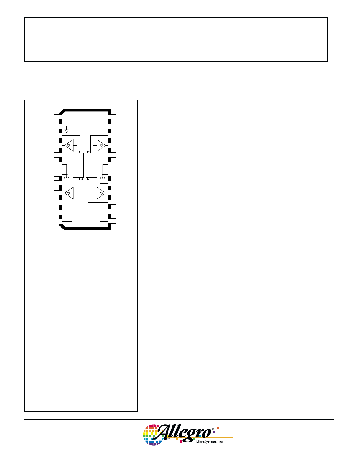
CONNECTION
LOGIC
GROUND
OUT
LOAD
SUPPLY
GROUND
GROUND
SENSE
OUT
PWM
NO
S
S
CP1
1
NC
2
10
3
4
1A
5
1
V
BB1
6
7
1
8
9
1B
9
10
11
11
1
12
LOGIC
CHARGE PUMP
LOGIC
24
DD
V
23
22
21
20
V
BB2
19
18
17
16
15
14
13
LOGIC
SUPPLY
2
PWM
S
20
OUT
2A
LOAD
SUPPLY
GROUND
GROUND
SENSE
OUT
2B
S
21
V
CP
CP2
Dwg. PP-069-2
DUAL DMOS
FULL-BRIDGE DRIVER
Designed to interface between external PWM control logic and
inductive loads such as relays, solenoids, dc motors, or stepper motors,
each full bridge can operate with output currents to ±2.5 A and operating
voltages to 50 V.
Low r
during PWM operation. Internal charge pump circuitry is used to create
a boosted voltage to fully enhance the high-side DMOS switches.
2
Three TTL-compatible logic-input terminals per bridge allow flexibility in configuring PWM control.
2
Internal circuit protection includes thermal shutdown with hysteresis,
and crossover-current protection. Special power -up sequencing is not
required.
The A3971SLB is supplied in a 24-lead plastic SOIC with a copper
batwing tab. The power tab is at ground potential and needs no electrical isolation.
DMOS output drivers provide low power dissipation
DS(on)
ABSOLUTE MAXIMUM RATINGS
at TA = +25°C
Load Supply Voltage, VBB................ 50 V
Output Current, I
Transient (<500 ns) ................... ±5 A
Logic Supply Voltage,
VDD............................................ 7.0 V
Sense Voltage, V
Logic Input Voltage Range,
VIN.................. -0.3 V to V
High-Side Gate Voltage ........... V
Package Power Dissipation,
PD............................................. 2.2 W
Operating Temperature Range,
TA............................. -20°C to +85°C
Junction Temperature, TJ............. +150°C
Storage Temperature Range,
TS........................... -55°C to +150°C
Output duty cycle, ambient temperature, and
heat sinking may limit current rating. Under
any set of conditions, do not exceed the
specified current rating or a junction temperature of 150 °C.
OUT
...................... 0.5 V
SENSE
DD
BB
+ 0.3 V
+ 8 V
FEATURES
■ ±2.5 A Load Current Capability per Bridge
■ Parallel Outputs for 5 A Load-Current Capability
■ Low r
Typically 325 mΩ source, 175 mΩ sink
■ Synchronous Rectification via Control Logic
■ Internal Undervoltage Monitor
■ Crossover-Current Protection
■ Source Connections for External Current Sensing
■ Thermal Shutdown Circuitry
Always order by complete part number: A3971SLB .
DS(on)
Outputs
Page 2
3971
DUAL DMOS
FULL-BRIDGE DRIVER
LOGIC
SUPPLY
V
DD
24
VOLTAGE
REFERENCE
FUNCTIONAL BLOCK DIAGRAM
0.22 µF/100 V
CP1CP2
12
V
REF
LOW SIDE SUPPLY
V
CP
13
CHARGE PUMP
DMOS H-BRIDGE
V
CP
14
V
BB2
20
0.22 µF
50 V
LOAD
SUPPLY
S
S
PWM
PWM
LGND
UVLO &
THERMAL
OUT
2A
21
SHUTDOWN
OUT
2B
16
3
10
10
11
11
1
BRIDGE 1
CONTROL
LOGIC
GATE
17
SENSE
(OPTIONAL)
2
RS, C
S
DRIVE
DMOS H-BRIDGE
22
S
20
15
S
21
23
2
2
BRIDGE 2
CONTROL
LOGIC
5
V
OUT
4
OUT
9
SENSE
8
BB1
1A
1B
(OPTIONAL)
1
R
,
C
S
S
GROUND
6
7
18
19
115 Northeast Cutoff, Box 15036
Worcester, Massachusetts 01615-0036 (508) 853-5000
Copyright © 2000, Allegro MicroSystems, Inc.
Dwg. FP-050
Page 3

3971
DUAL DMOS
FULL-BRIDGE DRIVER
ELECTRICAL CHARACTERISTICS at TA = +25°C, VBB = 50 V, VDD = 5.0 V (unless otherwise noted).
Limits
Characteristic Symbol Test Conditions Min. Typ. Max. Units
Load Supply Voltage Range V
Logic Supply Voltage Range V
Load Supply Current I
Logic Supply Current I
Output Drivers
Output Leakage Current I
Output ON Resistance r
DS(on)
Body Diode Forward Voltage V
High-Side Gate Voltage V
Control Logic
Logic Input Voltage V
V
Logic Input Current I
I
Propagation Delay Time t
BB
DD
BB
DD
DSS
F
CP
IN(0)
IN(1)
IN(0)
IN(1)
PD
Operating 10 — 50 V
Operating 4.5 5.0 5.5 V
Operating, each supply, no load — — 3.0 mA
Operating — — 5.0 mA
V
= V
OUT
V
OUT
High-side switch, I
Low-side switch, I
BB
= 0 V — <-1.0 -20 mA
= -2.5 A — 325 375 mΩ
OUT
= 2.5 A — 175 200 mΩ
OUT
— <1.0 20 µA
Source diode, IF = 2.5 A — 1.2 — V
Sink diode, IF = 2.5 A — 1.0 — V
C = 0.22 µF, reference V
BB
6.0 6.5 7.0 V
——0.8V
2.0 — — V
VIN = 0 V — <1.0 -5.0 µA
VIN = 5.0 V — 20 50 µA
50% to 90%:
PWM change to source off — 50 — ns
PWM change to sink off — 60 — ns
PWM change to source on — 565 — ns
PWM change to sink on — 665 — ns
Disable to source on — 150 — ns
Disable to sink on — 250 — ns
Thermal Shutdown Temperature T
Thermal Shutdown Hysteresis ∆T
UVLO Threshold V
UVLO Hysteresis ∆V
J
J
UVLO
UVLO
Increasing V
NOTES: 1. Typical Data is for design information only.
2. Negative current is defined as coming out of (sourcing) the specified device terminal.
www.allegromicro.com
DD
— 165 — °C
—15—°C
3.9 4.15 4.4 V
—0.15— V
Page 4

3971
DUAL DMOS
FULL-BRIDGE DRIVER
Logic Truth Table
PWM
x
S
x0
S
x1
OUT
xA
OUT
xB
Function
X 0 0 Z Z Disable
001LH Forward
0 1 0 H L Reverse
011LLSynchronous
101LLRectification/
111LLSlow Decay
110LL Chop
Terminal List
Terminal Name Description
1 NC No (Internal) connection
2 LGND Logic ground
3S10Control input, bridge 1
4 OUT
5V
1A
BB1
6, 7 GND Ground
8 SENSE
9 OUT
10 S
11 PWM
1
1B
11
1
12 CP1 Charge-pump capacitor
13 CP2 Charge-pump capacitor
14 V
15 S
16 OUT
17 SENSE
CP
21
2B
2
18, 19 GND Ground
20 V
21 OUT
22 S
23 PWM
24 V
BB2
2A
20
2
DD
Output A, bridge 1
Load supply voltage, bridge 1
Sense resistor, bridge 1
Output B, bridge 1
Control input, bridge 1
Control input, bridge 1
Reservoir capacitor
Control input, bridge 2
Output B, bridge 2
Sense resistor, bridge 2
Load supply voltage, bridge 2
Output A, bridge 2
Control input, bridge 2
Control input, bridge 2
Logic supply voltage
115 Northeast Cutoff, Box 15036
Worcester, Massachusetts 01615-0036 (508) 853-5000
Page 5

Functional Description
3971
DUAL DMOS
FULL-BRIDGE DRIVER
Charge Pump. The DMOS output stage requires a
charge pump to bring the high-side gate-source voltage
approximately 8 V above the V
supply. Two external
BB
components are required, a pumping capacitor connected
between CP1 and CP2 and a reservoir capacitor connected
between V
and VCP. Ceramic 0.22 µF capacitors are
BB
recommended.
Control Logic. Each bridge is controlled by three TTLcompatible inputs. The inputs are resistively pulled to
ground (via 250 kΩ). A crossover-delay circuit protects
the outputs from a shoot-thru condition when going from a
forward or reverse on state to synchronous rectification/
slow decay chop (both sink drivers on). If the logic is in
the DISABLE state and changes to an on state the 415 ns
crossover delay does not occur.
Protection Circuitry. In the event of a fault due to
excessive junction temperature, or low voltage on V
CP
or
VDD, the outputs of the device are disabled until the fault
condition is removed.
Current Sensing. If external current-sensing circuitry
is used, the sense resistor should have an independent
ground return to the ground terminal of the device. Due to
current transients during switching, a 0.1 µF capacitor
should be connected from the sense terminal to the
batwing tab connection of the package. This capacitor
reduces voltage swings at the terminal due to the fast di/dt,
which in turn ensures that the sink driver gate-source
voltage stays within the safe operating area. Allegro
MicroSystems recommends a value of R
R
S
= 0.5/I
TRIP
max.
given by:
S
Thermal protection. Circuitry turns off all drivers
when the junction temperature reaches 165°C, typically.
It is intended only to protect the device from failures due
to excessive junction temperatures and should not imply
that output short circuits are permitted. Thermal shutdown has a hysteresis of approximately 15°C.
Layout. The printed wiring board should use a heavy
ground plane. For optimum electrical and thermal performance, the driver should be soldered directly onto the
board. If external current sensing is used, the ground side
should have an individual path to the ground
of R
S
terminal(s) of the device. This path should be as short as
is possible physically and should not have any other
components connected to it. The load supply terminal
should be decoupled with an electrolytic capacitor
( >47 µF is recommended) placed as close to the device as
is possible.
Parallel Operation. For high-power applications, the
two DMOS full bridges in the A3971 may be connected in
parallel as shown below. The current will be shared
equally in each full bridge due to the positive temperature
coefficient of the DMOS
PWM
CONTROL
15–50 V
+
47 µF
0.22 µF
1
2
3
4
5
6
7
8
9
9
10
11
12
r
NC
V
BB1
CHARGE PUMP
DS(on)
LOGIC
.
LOGIC
24
V
DD
23
22
21
20
V
BB2
19
18
17
16
15
14
13
+5 V
15–50 V
+
47 µF
0.22 µF
www.allegromicro.com
Dwg. EP-069
Page 6

3971
DUAL DMOS
FULL-BRIDGE DRIVER
Dimensions in Inches
(for reference only)
0.2992
0.2914
0.020
0.013
0.0926
0.1043
24 13
1 2
0.0040
3
0.6141
0.5985
MIN.
0.050
BSC
0.0125
0.0091
0.419
0.394
0.050
0.016
0° TO 8°
Dwg. MA-008-24A in
NOTES:1. Exact body and lead configuration at vendor’s option within limits shown.
2. Lead spacing tolerance is non-cumulative
3. Webbed lead frame. Leads 6, 7, 18, and 19 are internally one piece.
115 Northeast Cutoff, Box 15036
Worcester, Massachusetts 01615-0036 (508) 853-5000
Page 7

Dimensions in Millimeters
(controlling dimensions)
3971
DUAL DMOS
FULL-BRIDGE DRIVER
7.60
7.40
0.51
0.33
2.65
2.35
24
1
0.10
2
MIN.
13
10.65
10.00
3
15.60
15.20
1.27
BSC
0° TO 8°
0.32
0.23
1.27
0.40
Dwg. MA-008-24A mm
NOTES:1. Exact body and lead configuration at vendor’s option within limits shown.
2. Lead spacing tolerance is non-cumulative
3. Webbed lead frame. Leads 6, 7, 18, and 19 are internally one piece.
www.allegromicro.com
Page 8

3971
DUAL DMOS
FULL-BRIDGE DRIVER
The products described here are manufactured under one or more
U.S. patents or U.S. patents pending.
Allegro MicroSystems, Inc. reserves the right to make, from time to
time, such departures from the detail specifications as may be
required to permit improvements in the performance, reliability, or
manufacturability of its products. Before placing an order, the user is
cautioned to verify that the information being relied upon is current.
Allegro products are not authorized for use as critical components
in life-support devices or systems without express written approval.
The information included herein is believed to be accurate and
reliable. However, Allegro MicroSystems, Inc. assumes no responsibility for its use; nor for any infringement of patents or other rights of
third parties which may result from its use.
115 Northeast Cutoff, Box 15036
Worcester, Massachusetts 01615-0036 (508) 853-5000
 Loading...