

Page 1
3968
Data Sheet
29319.29
ADVANCE INFORMATION
(subject to change without notice)
September 3, 1999
A3968SLB
OUT
INPUT
INPUT
GROUND
SENSE
OUT
SUPPLY
REFERENCE
1
1A
V
2
1A
3
1B
4
5
1
6
1B
LOAD
710
89
REF
BB
LOGICLOGIC
V
BB
ABSOLUTE MAXIMUM RATINGS
Load Supply Voltage, VBB................... 30 V
Output Current, I
(continuous) .............................. ±650 mA
Logic Supply Voltage, VCC................. 7.0 V
Input Voltage, Vin..... -0.3 V to VCC + 0.3 V
Sense Voltage, VS................................ 1.0 V
Package Power Dissipation
A3968SA ................................... 2.08 W*
A3968SLB ................................. 1.87 W*
Operating Temperature Range,
TA................................... -20°C to +85°C
Junction Temperature,
TJ................................................. +150°C
Storage Temperature Range,
TS................................. -55°C to +150°C
Output current rating may be limited by duty
cycle, ambient temperature, and heat sinking.
Under any set of conditions, do not exceed the
specified current rating or a junction temperature
of 150°C.
* Per SEMI G42-88 Specification, Thermal Test
Board Standardization for Measuring Junctionto-Ambient Thermal Resistance of Semiconductor
Packages.
(peak) .......... ±750 mA
OUT
16
15
14
13
12
11
V
CC
RC
Dwg. PP-066
(TA = 25°C)
OUT
INPUT
INPUT
GROUND
SENSE
OUT
LOGIC
SUPPLY
RCV
, P
DUAL FULL-BRIDGE PWM
MOTOR DRIVER WITH BRAKE
The A3968SA and A3968SLB are designed to bidirectionally control two
dc motors. Each device includes two H-bridges capable of continuous output
currents of ±650 mA and operating voltages to 30 V. Motor winding current
can be controlled by the internal fixed-frequency, pulse-width modulated
2A
2A
2B
2
2B
D
(PWM), current-control circuitry. The peak load current limit is set by the
user’s selection of a reference voltage and current-sensing resistors. Except
for package style and pinout, the two devices are identical.
The fixed-frequency pulse duration is set by a user-selected external
RC timing network. The capacitor in the RC timing network also determines
a user-selectable blanking window that prevents false triggering of the PWM
current-control circuitry during switching transitions.
To reduce on-chip power dissipation, the H-bridge power outputs have
been optimized for low saturation voltages. The sink drivers feature Allegro’s
patented Satlington™ output structure. The Satlington outputs combine the
low voltage drop of a saturated transistor and the high peak current capability
of a Darlington.
For each bridge, the INPUT
and INPUTB terminals determine the load
A
current polarity by enabling the appropriate source and sink driver pair.
When a logic low is applied to both INPUTs of a bridge, the braking function
is enabled. In brake mode, both source drivers are turned OFF and both sink
drivers are turned ON, thereby dynamically braking the motor. When a logic
high is applied to both INPUTs of a bridge, all output drivers are disabled.
Special power-up sequencing is not required. Internal circuit protection
includes thermal shutdown with hysteresis, ground-clamp and flyback diodes,
and crossover-current protection.
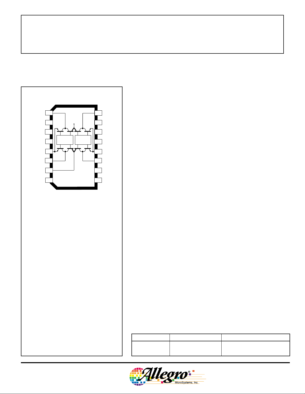
The A3968SA is supplied in a 16-pin dual in-line plastic package. The
A3968SLB is supplied in a 16-lead plastic SOIC with copper heat sink tabs.
The power tab is at ground potential and needs no electrical isolation.
FEATURES
■ ±650 mA Continuous Output Current
■ 30 V Output Voltage Rating
■ Internal Fixed-Frequency PWM Current Control
■ Satlington™ Sink Drivers
■ Brake Mode
■ User-Selectable Blanking Window
■ Internal Ground-Clamp & Flyback Diodes
■ Internal Thermal-Shutdown Circuitry
■ Crossover-Current Protection and UVLO Protection
Always order by complete part number:
Part Number Package R
θJA
A3968SA 16-pin DIP 60°C/W 38°C/W —
A3968SLB 16-lead batwing SOIC 67°C/W — 6°C/W
R
θJC
R
θJT
Page 2
3968
DUAL FULL-BRIDGE
PWM MOTOR DRIVER
WITH BRAKE
FUNCTIONAL BLOCK DIAGRAM
(one-half of circuit shown)
INPUT
UVLO
& TSD
INPUT
GROUND
A
LOGIC
SUPPLY
V
A
CC
OUT
V
BB
B
OUT
LOAD
SUPPLY
+
CONTROL LOGIC
B
R
T
SOURCE
ENABLE
RC
PWM LATCH
Q
C
T
OSC
BLANKING
GATE
R
S
CURRENT-SENSE
COMPARATOR
TO OTHER
BRIDGE
TO OTHER
BRIDGE
SENSE
+
–
TO OTHER
BRIDGE
÷4
REFERENCE
R
S
Dwg. FP-036-4
SENSE
OUT
LOAD
SUPPLY
REFERENCE
RC
LOGIC
SUPPLY
OUT
SENSE
A3968SA
TRUTH TABLE
INPUT
1
1
2
1B
3
V
4
REF
RC
5
V
6
CC
7
2B
8
2
V
LOGIC
BB
LOGIC
16
15
14
13
12
11
10
9
Dwg. PP-066-3
INPUT
OUT
1B
1A
1A
INPUTAINPUT
OUT
B
LLLLBrake mode
L H L H “Forward”
H L H L “Reverse”
H H Z Z Disable
GROUND
GROUND
OUT
2A
INPUT
2A
INPUT
2B
115 Northeast Cutoff, Box 15036
Worcester, Massachusetts 01615-0036 (508) 853-5000
Copyright © 1998, Allegro MicroSystems, Inc.
Z = High impedance
OUT
A
B
Description
Page 3
3968
DUAL FULL-BRIDGE
PWM MOTOR DRIVER
WITH BRAKE
ELECTRICAL CHARACTERISTICS at T
V
= 0 V, 56 kΩ & 680 pF RC to Ground (unless noted otherwise)
S
= +25°C, V
A
= 30 V, VCC = 4.75 V to 5.5 V, V
BB
REF
= 2 V,
Limits
Characteristic Symbol Test Conditions Min. Typ. Max. Units
Output Drivers
Load Supply Voltage Range V
Output Leakage Current I
Output Saturation Voltage V
CE(SAT)
Clamp Diode Forward Voltage V
Motor Supply Current I
(No Load)
BB(ON)
I
BB(OFF)
BB
CEX
F
Operating, I
V
= 30 V — <1.0 50 µA
OUT
V
= 0 V — <-1.0 -50 µA
OUT
Source Driver, I
Source Driver, I
Sink Driver, I
Sink Driver, I
= ±650 mA, L = 3 mH V
OUT
= -400 mA — 1.7 2.0 V
OUT
= -650 mA — 1.8 2.1 V
OUT
= +400 mA, VS = 0.5 V — 0.3 0.5 V
OUT
= +650 mA, VS = 0.5 V — 0.4 1.3 V
OUT
CC
—30 V
IF = 400 mA — 1.1 1.4 V
IF = 650 mA — 1.4 1.6 V
Both bridges ON (forward or reverse) — 3.0 5.0 mA
All INPUTs = 2.4 V — <1.0 200 µA
Control Logic
Logic Supply Voltage Range V
Logic Input Voltage V
V
Logic Input Current I
Reference Input Volt. Range V
Reference Input Current I
Reference Divider Ratio V
REF/VTRIP
Current-Sense Comparator V
IN(1)
I
IN(0)
REF
CC
IN(1)
IN(0)
REF
IO
Operating 4.75 — 5.50 V
V
IN
V
IN
Operating 0.1 – 2.0 V
V
REF
Input Offset Voltage
Current-Sense Comparator V
S
Operating -0.3 — 1.0 V
Input Voltage Range
Sense-Current Offset I
SO
IS – I
NOTES: 1. Typical Data is for design information only.
2. Negative current is defined as coming out of (sourcing) the specified device terminal.
2.4 — — V
— — 0.8 V
= 2.4 V — <1.0 20 µA
= 0.8 V — <-20 -200 µA
-2.5 0 1.0 µA
3.8 4.0 4.2 —
= 0.1 V -6.0 0 6.0 mV
, 50 mA ≤ I
OUT
≤ 650 mA 12 18 24 mA
OUT
Page 4

3968
DUAL FULL-BRIDGE
PWM MOTOR DRIVER
WITH BRAKE
ELECTRICAL CHARACTERISTICS at T
V
= 0 V, 56 kΩ & 680 pF RC to Ground (unless noted otherwise) (cont.)
S
= +25°C, V
A
= 30 V, VCC = 4.75 V to 5.5 V, V
BB
REF
= 2 V,
Limits
Characteristic Symbol Test Conditions Min. Typ. Max. Units
Control Logic (continued)
PWM RC Frequency f
PWM Propagation Delay Time t
Cross-Over Dead Time t
Propagation Delay Times t
Thermal Shutdown Temp. T
Thermal Shutdown Hysteresis ∆T
UVLO Enable Threshold V
UVLO Hysteresis V
Logic Supply Current I
osc
PWM
codt
T(UVLO)+
T(UVLO)hys
CC(ON)
I
CC(OFF)
I
CC(BRAKE)
pd
J
J
CT = 680 pF, R
Comparator Trip to Source OFF — 1.0 1.4 µs
Cycle Reset to Source ON — 0.8 1.2 µs
1 kΩ Load to 25 V 0.2 1.8 3.0 µs
I
= ±650 mA, 50% to 90%:
OUT
Disable OFF to Source ON — 100 — ns
Disable ON to Source OFF — 500 — ns
Disable OFF to Sink ON — 200 — ns
Disable ON to Sink OFF — 200 — ns
Brake Enable to Sink ON — 2200 — ns
Brake Enable to Source OFF — 200 — ns
Increasing V
Both bridges ON (forward or reverse) — — 50 mA
All INPUTs = 2.4 V — — 9.0 mA
All INPUTs = 0.8 V — — 95 mA
= 56 kΩ 22.9 25.4 27.9 kHz
T
— 165 — °C
—15—°C
CC
— 4.1 4.6 V
0.1 0.6 — V
NOTES: 1. Typical Data is for design information only.
2. Negative current is defined as coming out of (sourcing) the specified device terminal.
115 Northeast Cutoff, Box 15036
Worcester, Massachusetts 01615-0036 (508) 853-5000
Page 5

FUNCTIONAL DESCRIPTION
3968
DUAL FULL-BRIDGE
PWM MOTOR DRIVER
WITH BRAKE
Internal PWM Current Control. The A3968SA and
A3968SLB dual H-bridges are designed to bidirectionally
control two dc motors. An internal fixed-frequency PWM
current-control circuit controls the load current in each
motor. The current-control circuitry works as follows:
when the outputs of the H-bridge are turned on, current
increases in the motor winding. The load current is sensed
by the current-control comparator via an external sense
resistor (R
). Load current continues to increase until it
S
reaches the predetermined value, set by the selection of
external current-sensing resistors and reference input
voltage (V
where I
) according to the equation:
REF
= I
I
TRIP
is the sense-current error (typically 18 mA) due
SO
+ ISO = V
OUT
REF
/(4 RS)
to the base-drive current of the sink driver transistor.
At the trip point, the comparator resets the sourceenable latch, turning off the source driver of that H-bridge.
The source turn off of one H-bridge is independent of the
other H-bridge. Load inductance causes the current to
recirculate through the sink driver and ground-clamp
diode. The current decreases until the internal clock
oscillator sets the source-enable latches of both H-bridges,
turning on the source drivers of both bridges. Load current
increases again, and the cycle is repeated.
The frequency of the internal clock oscillator is set by
INPUT
A
the external timing components RTCT. The frequency can
be approximately calculated as:
= 1/(RT CT + t
f
osc
where t
is defined below.
blank
The range of recommended values for R
blank
)
and CT are
T
20 kΩ to 100 kΩ and 470 pF to 1000 pF respectively.
Nominal values of 56 kΩ and 680 pF result in a clock
frequency of 25.4 kHz.
Current-Sense Comparator Blanking. When the
source driver is turned on, a current spike occurs due to
the reverse-recovery currents of the clamp diodes and
switching transients related to distributed capacitance in
the load. To prevent this current spike from erroneously
resetting the source enable latch, the current-control
comparator output is blanked for a short period of time
when the source driver is turned on. The blanking time is
set by the timing component C
according to the equa-
T
tion:
t
= 1900 CT (µs).
blank
A nominal C
value of 680 pF will give a blanking
T
time of 1.3 µs.
The current-control comparator is also blanked when
the load current changes polarity (direction or phase
change). This internally generated blank time is approximately 1.8 µs.
INPUT
I
OUTB
B
"FORWARD" "REVERSE"
BRIDGE
+
0
–
ON
BRIDGE
INTERNAL
OSCILLATOR
ON
ALL
OFF
SOURCE
I
TRIP
OFF
t
d
R C
T T
t
blank
Dwg. WM-003-3
V
BB
BRIDGE ON
SOURCE OFF
ALL OFF
R
S
Dwg. EP-006-16
Page 6

3968
DUAL FULL-BRIDGE
PWM MOTOR DRIVER
WITH BRAKE
FUNCTIONAL DESCRIPTION (continued)
Load Current Regulation. Due to internal logic and
switching delays (t
slightly higher than the I
), the actual load current peak may be
d
value. These delays, plus the
TRIP
blanking time, limit the minimum value the current control
circuitry can regulate. To produce zero current in a
winding, the INPUTA and INPUTB terminals should be
held high, turning off all output drivers for that H-bridge.
Logic Inputs. The direction of current in the motor
winding is determined by the state of the INPUT
A
and
INPUTB terminals of each bridge (see Truth Table). An
internally generated dead time (t
) of approximately
codt
1.8 µs prevents cross-over current spikes that can occur
when switching the motor direction.
A logic high on both INPUTs turns off all four output
drivers of that H-bridge. This results in a fast current
decay through the internal ground clamp and flyback
diodes.
The appropriate INPUT
or INPUTB can be pulse-
A
width modulated for applications that require a fast current-decay PWM. The internal current-control logic can be
disabled by connecting the RTCT terminal to ground.
A logic low on the INPUTA and the INPUTB terminals
will place that H-Bridge in the brake mode. Both source
drivers are turned OFF and both sink drivers are turned
ON. This has the effect of shorting the dc motor’s backEMF voltage, resulting in a current flow that dynamically
brakes the motor.
Note that during braking the internal current-control
circuitry is disabled. Therefore, care should be taken to
ensure that the motor’s current does not exceed the absolute maximum rating of the A3968.
The REFERENCE input voltage is typically set with a
resistor divider from V
. This reference voltage is
CC
internally divided down by 4 to set up the current-comparator trip-voltage threshold. The reference input voltage
range is 0 to 2 V.
Output Drivers. To minimize on-chip power dissipation, the sink drivers incorporate a Satlington™ structure.
The Satlington output combines the low V
CE(sat)
features
of a saturated transistor and the high peak-current capability of a Darlington (connected) transistor. A graph
showing typical output saturation voltages as a function
of output current is on the next page.
Miscellaneous Information. Thermal protection
circuitry turns off all output drivers should the junction
temperature reach +165 °C (typical). This is intended
only to protect the device from failures due to excessive
junction temperatures and should not imply that output
short circuits are permitted. Normal operation is resumed
when the junction temperature has decreased about 15 °C.
The A3968 current control employs a fixed-frequency, variable duty cycle PWM technique. If the duty
cycle exceeds 50%, the current-control-regulation frequency may change.
To minimize current-sensing inaccuracies caused by
ground trace I
drops, each current-sensing resistor
R
should have a separate return to the ground terminal of
the device. For low-value sense resistors, the I•R drops
in the printed-wiring board can be significant and should
be taken into account. The use of sockets should be
avoided as their contact resistance can cause variations in
the effective value of RS.
The LOAD SUPPLY terminal, VBB, should be
decoupled with an electrolytic capacitor (47 µF recommended) placed as close to the device as physically
practical. To minimize the effect of system ground IR
drops on the logic and reference input signals, the system
ground should have a low-resistance return to the load
supply voltage.
The frequency of the clock oscillator will determine
the amount of ripple current. A lower frequency will
result in higher current ripple, but reduced heating in the
motor and driver IC due to a corresponding decrease in
hysteretic core losses and switching losses respectively.
A higher frequency will reduce ripple current, but will
increase switching losses and EMI.
115 Northeast Cutoff, Box 15036
Worcester, Massachusetts 01615-0036 (508) 853-5000
Page 7

2.5
2.0
3968
DUAL FULL-BRIDGE
PWM MOTOR DRIVER
WITH BRAKE
TA = +25°C
SOURCE DRIVER
Typical output saturation
voltages showing Satlington™
sink-driver operation.
TYPICAL APPLICATION
MOTOR
1
1
INPUT
INPUT
1A
1B
2
3
1.5
1.0
0.5
SINK DRIVER
OUTPUT SATURATION VOLTAGE IN VOLTS
0
200
OUTPUT CURRENT IN MILLIAMPERES
16
V
BB
15
14
INPUT
INPUT
2A
2B
400 700300
500
MOTOR
600
Dwg. GP-064-1
2
+5 V
4
0.5 Ω
5
6
+24 V
39 kΩ
47 µF
10 kΩ
710
V
89
REF
+
Dwg. EP-047-6
LOGICLOGIC
V
BB
13
0.5 Ω
12
11
V
CC
RC
+5 V
680 pF
56 kΩ
Page 8

3968
DUAL FULL-BRIDGE
PWM MOTOR DRIVER
WITH BRAKE
THIS PAGE INTENTIONALLY LEFT BLANK
115 Northeast Cutoff, Box 15036
Worcester, Massachusetts 01615-0036 (508) 853-5000
Page 9

0.280
0.240
3968
DUAL FULL-BRIDGE
PWM MOTOR DRIVER
WITH BRAKE
A3968SA
Dimensions in Inches
(controlling dimensions)
0.014
16
9
0.008
0.300
BSC
0.430
MAX
0.210
MAX
7.11
6.10
0.015
MIN
1
0.070
0.045
16
0.022
0.014
8
0.775
0.735
0.100
BSC
Dimensions in Millimeters
(for reference only)
0.005
MIN
0.150
0.115
Dwg. MA-001-16A in
0.355
9
0.204
7.62
BSC
10.92
MAX
8
0.13
MIN
3.81
2.93
5.33
MAX
0.39
MIN
1
1.77
1.15
0.558
0.356
19.68
18.67
2.54
BSC
NOTES: 1. Exact body and lead configuration at vendor’s option within limits shown.
2. Lead spacing tolerance is non-cumulative
3. Lead thickness is measured at seating plane or below.
Dwg. MA-001-16A mm
Page 10

3968
DUAL FULL-BRIDGE
PWM MOTOR DRIVER
WITH BRAKE
16 9
A3968SLB
Dimensions in Inches
(for reference only)
0.0125
0.0091
0.2992
0.2914
0.020
0.013
0.0926
0.1043
7.60
7.40
1 2
0.0040 MIN.
3
0.4133
0.3977
Dimensions in Millimeters
(controlling dimensions)
916
0.050
BSC
0.419
0.394
10.65
10.00
0° TO 8°
0.050
0.016
Dwg. MA-008-16A in
0.32
0.23
0.51
0.33
2.65
2.35
1 2
0.10
MIN.
3
10.50
10.10
1.27
BSC
NOTES: 1. Exact body and lead configuration at vendor’s option within limits shown.
2. Lead spacing tolerance is non-cumulative
3. Webbed lead frame. Leads 4 and 13 are internally one piece.
115 Northeast Cutoff, Box 15036
Worcester, Massachusetts 01615-0036 (508) 853-5000
0° TO 8°
1.27
0.40
Dwg. MA-008-16A mm
Page 11

3968
DUAL FULL-BRIDGE
PWM MOTOR DRIVER
WITH BRAKE
Allegro MicroSystems, Inc. reserves the right to make, from time to
time, such departures from the detail specifications as may be required
to permit improvements in the design of its products.
The information included herein is believed to be accurate and
reliable. However, Allegro MicroSystems, Inc. assumes no responsibility for its use; nor for any infringements of patents or other rights of
third parties which may result from its use.
Page 12

3968
DUAL FULL-BRIDGE
PWM MOTOR DRIVER
WITH BRAKE
MOTOR DRIVERS SELECTION GUIDE
Function Output Ratings* Part Number
INTEGRATED CIRCUITS FOR BRUSHLESS DC MOTORS
3-Phase Power MOSFET Controller — 28 V 3933
3-Phase Power MOSFET Controller — 50 V 3932
3-Phase Power MOSFET Controller — 50 V 7600
2-Phase Hall-Effect Sensor/Driver 400 mA 26 V 3626
Bidirectional 3-Phase Back-EMF Controller/Driver ±600 mA 14 V 8906
2-Phase Hall-Effect Sensor/Driver 900 mA 14 V 3625
3-Phase Back-EMF Controller/Driver ±900 mA 14 V 8902–A
3-Phase Controller/Drivers ±2.0 A 45 V 2936 & 2936-120
INTEGRATED BRIDGE DRIVERS FOR DC AND BIPOLAR STEPPER MOTORS
Dual Full Bridge with Protection & Diagnostics ±500 mA 30 V 3976
PWM Current-Controlled Dual Full Bridge ±650 mA 30 V 3966
PWM Current-Controlled Dual Full Bridge ±650 mA 30 V 3968
PWM Current-Controlled Dual Full Bridge ±750 mA 45 V 2916
PWM Current-Controlled Dual Full Bridge ±750 mA 45 V 2919
PWM Current-Controlled Dual Full Bridge ±750 mA 45 V 6219
PWM Current-Controlled Dual Full Bridge ±800 mA 33 V 3964
PWM Current-Controlled Full Bridge ±1.3 A 50 V 3953
PWM Current-Controlled Dual Full Bridge ±1.5 A 45 V 2917
PWM Current-Controlled Dual Full Bridge ±1.5 A 45 V 2918
PWM Current-Controlled Microstepping Full Bridge ±1.5 A 50 V 3955
PWM Current-Controlled Microstepping Full Bridge ±1.5 A 50 V 3957
PWM Current-Controlled Dual DMOS Full Bridge ±1.5 A 50 V 3972
Dual Full-Bridge Driver ±2.0 A 50 V 2998
PWM Current-Controlled Full Bridge ±2.0 A 50 V 3952
DMOS Full Bridge PWM Driver ±2.0 A 50 V 3958
PWM Current-Controlled Dual DMOS Full Bridge ±2.5 A 50 V 3971
UNIPOLAR STEPPER MOTOR & OTHER DRIVERS
Voice-Coil Motor Driver ±500 mA 6 V 8932–A
Voice-Coil Motor Driver ±800 mA 16 V 8958
Unipolar Stepper-Motor Quad Drivers 1 A 46 V 7024 & 7029
Unipolar Microstepper-Motor Quad Driver 1.2 A 46 V 7042
Unipolar Stepper-Motor Translator/Driver 1.25 A 50 V 5804
Unipolar Stepper-Motor Quad Driver 1.8 A 50 V 2540
Unipolar Stepper-Motor Quad Driver 1.8 A 50 V 2544
Unipolar Stepper-Motor Quad Driver 3 A 46 V 7026
Unipolar Microstepper-Motor Quad Driver 3 A 46 V 7044
* Current is maximum specified test condition, voltage is maximum rating. See specification for sustaining voltage limits
or over-current protection voltage limits. Negative current is defined as coming out of (sourcing) the output.
† Complete part number includes additional characters to indicate operating temperature range and package style.
Also, see 3175, 3177, 3235, and 3275 Hall-effect sensors for use with brushless dc motors.
†
115 Northeast Cutoff, Box 15036
Worcester, Massachusetts 01615-0036 (508) 853-5000
 Loading...