

Page 1
A3959
DMOS Full-Bridge PWM Motor Driver
Features and Benefits
▪ ±3 A, 50 V Output Rating
▪ Low r
Outputs (270 mΩ, Typical)
DS(on)
▪ Mixed, Fast, and Slow Current-Decay Modes
▪ Synchronous Rectification for Low Power Dissipation
▪ Internal UVLO and Thermal-Shutdown Circuitry
▪ Crossover-Current Protection
▪ Internal Oscillator for Digital PWM Timing
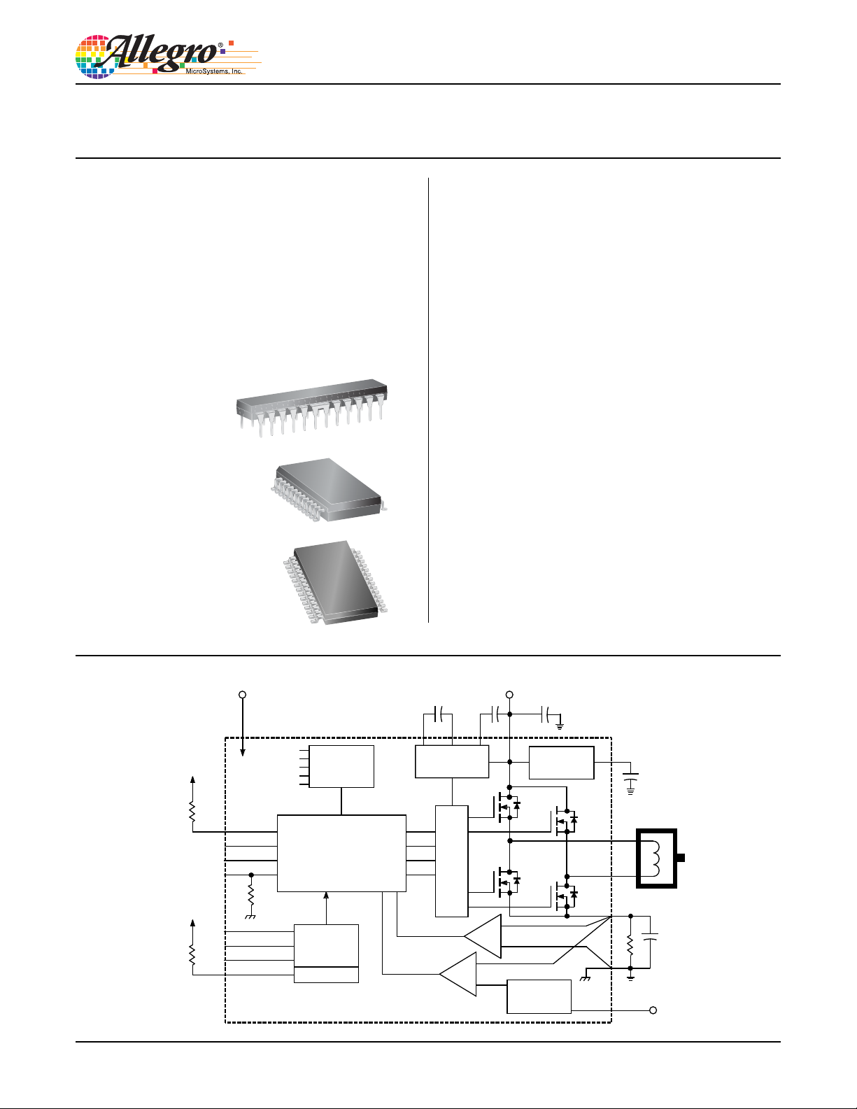
Packages:
Package B, 24-pin DIP
with exposed tabs
Package LB, 24-pin SOIC
with internally fused pins
Package LP, 28-pin TSSOP
with exposed thermal pad
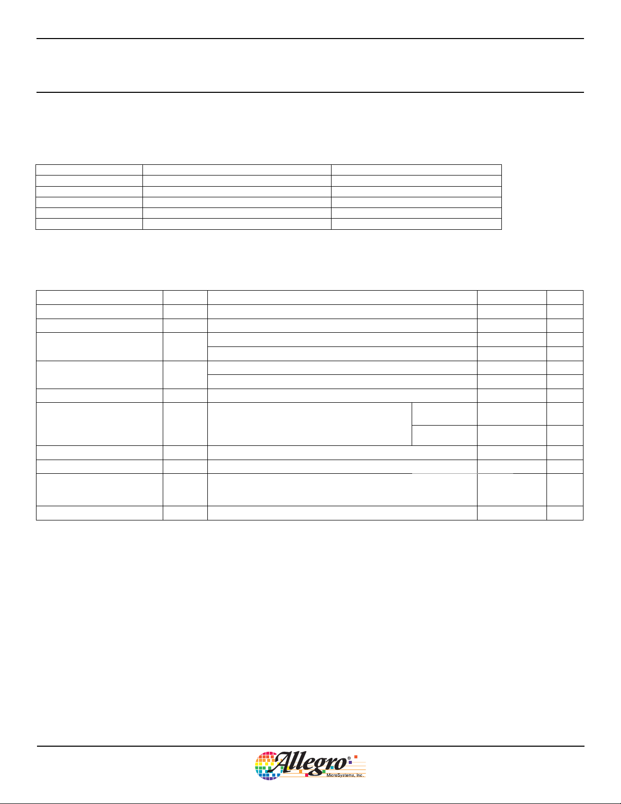
Description
Designed for pulse width modulated (PWM) current control of
DC motors, the A3959 is capable of output currents to ±3 A and
operating voltages to 50 V. Internal fixed off-time PWM currentcontrol timing circuitry can be adjusted via control inputs to
operate in slow, fast, and mixed current-decay modes.
PHASE and ENABLE input terminals are provided for use
in controlling the speed and direction of a DC motor with
externally applied PWM-control signals. Internal synchronous
rectification control circuitry is provided to reduce power
dissipation during PWM operation.
Internal circuit protection includes thermal shutdown with
hysteresis, undervoltage monitoring of supply and charge
pump, and crossover-current protection. Special power-up
sequencing is not required.
The A3959 provides a choice of three power packages, a 24-pin
DIP with batwing tabs (package suffix ‘B’), a 24-lead SOIC
with four internally-fused pins (package suffix ‘LB’), and a
thin (<1.2 mm) 28-pin TSSOP with an exposed thermal pad
(suffix ‘LP’). In all cases, the power pins and tabs are at ground
potential and need no electrical isolation. Each package is lead
(Pb) free, with 100% matte tin leadframes.
DD
TO V
SLEEP
EXT MODE
PHASE
ENABLE
TO V
DD
BLANK
PFD1
PFD2
ROSC
Not to scale
V
DD
LOGIC
SUPPLY
CHARGE PUMP
BANDGAP
V
C
REG
TSD
Functional Block Diagram
CP1
VOLTAGE &
DD
FAULT DETECT
CONTROL LOGIC
PWM
TIMER
OSC
UNDER-
CHARGE
PUMP
CURRENT
CP2
GATE DRIVE
SENSE
CP
ZERO
CURRENT
DETECT
V
BB
+
LOAD
SUPPLY
BANDGAP
REGULATOR
REFERENCE
BUFFER &
w10
V
REG
OUT
OUT
SENSE
REF
A
B
C
S
S
R
Dwg. FP-048-2A
V
REF
29319.37K
Page 2
A3959
DMOS Full-Bridge PWM Motor Driver
Selection Guide
Part Number Package Packing
A3959SB-T 24-pin DIP with exposed tabs 15 per tube
A3959SLB-T 24-pin SOIC with internally fused pins 31 per tube
A3959SLBTR-T 24-pin SOIC with internally fused pins 1000 per reel
A3959SLP-T 28-pin TSSOP with exposed thermal pad 50 per tube
A3959SLPTR-T 28-pin TSSOP with exposed thermal pad 4000 per reel
Absolute Maximum Ratings
Characteristic Symbol Notes Rating Units
Load Supply Voltage V
Logic Supply Voltage V
Input Voltage V
Sense Voltage V
Reference Voltage V
Output Current I
Package Power Dissipation P
Operating Ambient Temperature T
Maximum Junction Temperature TJ(max)
Storage Temperature T
BB
DD
IN
REF
OUT
stg
Continuous –0.3 to V
tw < 30 ns –1.0 to V
Continuous 0.5 V
S
t
< 3 μs 2.5 V
w
Output current rating may be limited by duty cycle, am-
bient temperature, and heat sinking. Under any set of
conditions, do not exceed the specifi ed current rating
or a junction temperature of 150°C.
See Thermal Characteristics – –
D
Range S –20 to 85 ºC
A
Fault conditions that produce excessive junction temperature will activate
the device’s thermal shutdown circuitry. These conditions can be toler-
ated but should be avoided.
50 V
7.0 V
+ 0.3 V
DD
+ 1.0 V
DD
V
DD
Repetitive ±3.0 A
Peak, < 3 μs ±6.0 A
150 ºC
–55 to 150 ºC
V
Allegro MicroSystems, Inc.
115 Northeast Cutoff
Worcester, Massachusetts 01615-0036 U.S.A.
1.508.853.5000; www.allegromicro.com
2
Page 3
A3959
0
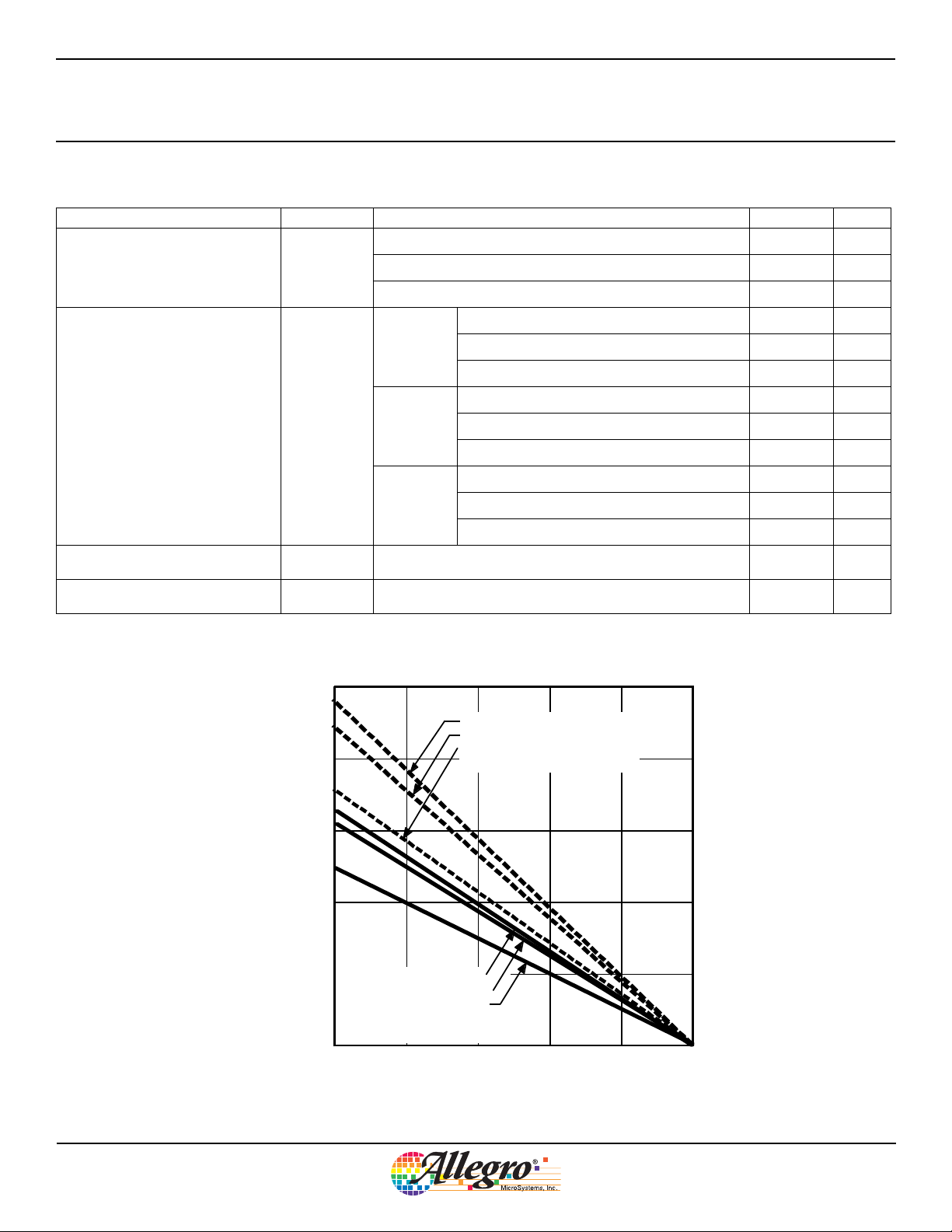
Thermal Characteristics
Characteristic Symbol Test Conditions Value Units
Package Power Dissipation P
Package Thermal Resistance, Junction
to Ambient
Package Thermal Resistance, Junction
to Tab
Package Thermal Resistance, Junction
to Pad
*Additional thermal information available on Allegro website.
D
R
θJA
R
θJT
R
θJP
DMOS Full-Bridge PWM Motor Driver
B package
LB package
LP package
1-layer PCB, minimal exposed copper area 54 ºC/W
B Package
LB Package
LP Package
B and LB packages 6 ºC/W
LP package 2 ºC/W
2-layer PCB, 1-in.2 2-oz copper exposed area 36 ºC/W
4-layer PCB, based on JEDEC standard 26 ºC/W
1-layer PCB, minimal exposed copper area 77 ºC/W
2-layer PCB, 1-in.2 2-oz copper exposed area 51 ºC/W
4-layer PCB, based on JEDEC standard 35 ºC/W
1-layer PCB, minimal exposed copper area 100 ºC/W
2-layer PCB, 1-in.2 2-oz copper exposed area 40 ºC/W
4-layer PCB, based on JEDEC standard 28 ºC/W
3.3 W
2.5 W
3.1 W
5
SUFFIX 'B', R
SUFFIX 'LP', R
4
SUFFIX 'LB', R
4-LAYER BOARD
QJA
QJA
QJA
= 26oC/W
= 28oC/W
= 35oC/W
3
2
1
SUFFIX 'B', R
SUFFIX 'LP', R
SUFFIX 'LB', R
2-LAYER BOARD,
1 SQ. IN. COPPER EA. SIDE
ALLOWABLE PACKAGE POWER DISSIPATION (W)
0
25
QJA
= 36oC/W
QJA
= 40oC/W
QJA
= 51oC/W
50 75 100 125 15
TEMPERATURE IN ooooC
Allegro MicroSystems, Inc.
115 Northeast Cutoff
Worcester, Massachusetts 01615-0036 U.S.A.
1.508.853.5000; www.allegromicro.com
3
Page 4

A3959
DMOS Full-Bridge PWM Motor Driver
Allegro MicroSystems, Inc.
115 Northeast Cutoff
Worcester, Massachusetts 01615-0036 U.S.A.
1.508.853.5000; www.allegromicro.com
4
Page 5

A3959
DMOS Full-Bridge PWM Motor Driver
ELECTRICAL CHARACTERISTICS (continued) at TA = +25°C, VBB = 50 V, VDD = 5.0 V, V
f
< 50 kHz (unless noted otherwise)
PWM
SENSE
= 0.5 V,
Characteristics Symbol Test Conditions Min. Typ. Max. Units
Reference Divider Ratio – – 10 – –
Gm Error
(Note 3)
= V
REF
E
Gm
V
0.5 Ein to 0.9 E
DD
= 0.5 V – – ±14 %
REF
:
out
– – ±4.0 %
V
PWM change to source on 600 750 1200 ns
Propagation Delay Times t
pd
PWM change to source off 50 150 350 ns
PWM change to sink on 600 750 1200 ns
PWM change to sink off 50 100 150 ns
Thermal Shutdown Temp. T
Thermal Shutdown Hysteresis ∆T
J
J
UVLO Enable Threshold UVLO Increasing V
DD
– 165 – °C
–15 – °C
3.90 4.2 4.45 V
UVLO Hysteresis ∆UVLO 0.05 0.10 – V
NOTES: 1. Typical Data is for design information only.
2. Negative current is defi ned as coming out of (sourcing) the specifi ed device terminal.
3. Gm error = ([V
REF
/10] – V
SENSE
)/(V
/10) where V
REF
SENSE
= I
TRIP•RS
.
Allegro MicroSystems, Inc.
115 Northeast Cutoff
Worcester, Massachusetts 01615-0036 U.S.A.
1.508.853.5000; www.allegromicro.com
5
Page 6

A3959
DMOS Full-Bridge PWM Motor Driver
FUNCTIONAL DESCRIPTION
V
. This internally generated voltage is used to operate
REG
the sink-side DMOS outputs. The V
be decoupled with a 0.22 μF capacitor to ground. V
terminal should
REG
REG
is
internally monitored and in the case of a fault condition,
the outputs of the device are disabled.
Charge Pump. The charge pump is used to generate a
gate-supply voltage greater than V
to drive the source-
BB
side DMOS gates. A 0.22 μF ceramic capacitor should be
connected between CP1 and CP2 for pumping purposes.
A 0.22 μF ceramic capacitor should be connected between
CP and V
to act as a reservoir to operate the high-side
BB
DMOS devices. The CP voltage is internally monitored
and, in the case of a fault condition, the source outputs of
the device are disabled.
PHASE Logic. The PHASE input terminal determines if
the device is operating in the “forward” or “reverse” state.
PHASE OUT
OUT
A
B
0 Low High
1 High Low
ENABLE Logic. The ENABLE input terminal allows
external PWM. ENABLE high turns on the selected sinksource pair. ENABLE low switches off the source driver
or the source and sink driver, depending on EXT MODE,
and the load current decays. If ENABLE is kept high, the
current will rise until it reaches the level set by the internal
current-control circuit.
ENABLE Outputs
0 Chopped
1 On
EXT MODE Logic. When using external PWM current
control, the EXT MODE input determines the current path
during the chopped cycle. With EXT MODE low, fast
decay mode, the opposite pair of selected outputs will be
enabled during the off cycle. With EXT MODE high, slow
decay mode, both sink drivers are on with ENABLE low.
EXT MODE Decay
0 Fast
1 Slow
Current Regulation. Load current is regulated by an
internal fi xed off-time PWM control circuit. When the
outputs of the DMOS H bridge are turned on, the current
increases in the motor winding until it reaches a trip value
):
) and the
S
determined by the external sense resistor (R
applied analog reference voltage (V
= V
I
TRIP
REF
REF
/10R
S
At the trip point, the sense comparator resets the sourceenable latch, turning off the source driver. The load
inductance then causes the current to recirculate for the
fi xed off-time period. The current path during recirculation
is determined by the confi guration of slow/mixed/fast
current-decay mode via PFD1 and PFD2.
Oscillator. The PWM timer is based on an internal
oscillator set by a resistor connected from the R
terminal to V
. Typical value of 4 MHz is set with a
DD
OSC
51 kΩ resistor. The allowable range of the resistor is from
20 kΩ to 100 kΩ.
If R
= 204 x 109/R
f
OSC
is not pulled up to VDD, it must be shorted to
OSC
OSC
.
ground.
Fixed Off Time. The A3959 is set for a fi xed off time of
96 cycles of the internal oscillator, typically 24 μs with a
4 MHz oscillator.
Allegro MicroSystems, Inc.
115 Northeast Cutoff
Worcester, Massachusetts 01615-0036 U.S.A.
1.508.853.5000; www.allegromicro.com
6
Page 7

A3959
DMOS Full-Bridge PWM Motor Driver
FUNCTIONAL DESCRIPTION (continued)
Internal Current-Control Mode. Inputs PFD1 and
PFD2 determine the current-decay method after an
overcurrent event is detected at the SENSE input. In slowdecay mode, both sink drivers are turned on for the fi xed
off-time period. Mixed-decay mode starts out in fast-decay
mode for a portion (15% or 48%) of the fi xed off time, and
then is followed by slow decay for the remainder of the
period.
PFD2 PFD1 % t
Decay
off
0 0 0 Slow
0 1 15 Mixed
1 0 48 Mixed
1 1 100 Fast
PWM Blank Timer. When a source driver turns on, a
current spike occurs due to the reverse-recovery currents
of the clamp diodes and/or switching transients related to
distributed capacitance in the load. To prevent this current
spike from erroneously resetting the source-enable latch,
the sense comparator is blanked. The blank timer runs
after the off-time counter to provide the blanking function.
The blank timer is reset when ENABLE is chopped or
PHASE is changed. For external PWM control, a PHASE
change or ENABLE on will trigger the blanking function.
The duration is determined by the BLANK input and the
oscilator.
BLANK t
blank
the appropriate pair of DMOS outputs during the current
decay and effectively short out the body diodes with the
low r
driver. This will reduce power dissipation
DS(on)
signifi cantly and can eliminate the need for external
Schottky diodes.
Synchronous rectifi cation will prevent reversal of load
current by turning off all outputs when a zero-current level
is detected.
Shutdown. In the event of a fault (excessive junction
temperature, or low voltage on CP or V
) the outputs of
REG
the device are disabled until the fault condition is removed.
At power up, and in the event of low V
, the UVLO
DD
circuit disables the drivers.
Braking. The braking function is implemented by
driving the device in slow-decay mode via EXTMODE
and applying an enable chop command. Because it is
possible to drive current in either direction through the
DMOS drivers, this confi guration effectively shorts out
the motor-generated BEMF as long as the ENABLE
chop mode is asserted. It is important to note that the
internal PWM current-control circuit will not limit the
current when braking, because the current does not fl ow
through the sense resistor. The maximum brake current
can be approximated by V
BEMF/RL
. Care should be taken
to ensure that the maximum ratings of the device are not
exceeded in worst-case braking situations of high speed
and high inertial loads.
0 6/f
1 12/f
osc
osc
Synchronous Rectifi cation. When a PWM off cycle
is triggered, either by an ENABLE chop command or
internal fi xed off-time cycle, load current will recirculate
according to the decay mode selected by the control logic.
The A3959 synchronous rectifi cation feature will turn on
SLEEP Logic. The SLEEP input terminal is used to
minimize power consumption when when not in use.
This disables much of the internal circuitry including the
regulator and charge pump. Logic low will put the device
into sleep mode, logic high will allow normal operation.
Note: If the sleep mode is not used,
up resistor between the SLEEP terminal and V
Allegro MicroSystems, Inc.
115 Northeast Cutoff
Worcester, Massachusetts 01615-0036 U.S.A.
1.508.853.5000; www.allegromicro.com
connect a 5 kΩ pull-
.
DD
7
Page 8

A3959
DMOS Full-Bridge PWM Motor Driver
FUNCTIONAL DESCRIPTION (continued)
Current Sensing. To minimize inaccuracies in
sensing the I
current level, which may be caused by
TRIP
ground trace IR drops, the sense resistor should have an
independent ground return to the ground terminal of the
device. For low-value sense resistors the IR drops in the
PCB sense resistor’s traces can be signifi cant and should
be taken into account. The use of sockets should be
avoided as they can introduce variation in R
due to their
S
contact resistance.
The maximum value of R
is given as RS = 0.5/I
S
TRIP
.
Thermal Protection. Circuitry turns off all drivers
when the junction temperature reaches 165°C typically. It
is intended only to protect the device from failures due to
excessive junction temperatures and should not imply that
output short circuits are permitted. Thermal shutdown has
a hysteresis of approximately 15°C.
Layout. A star ground system located close to the driver
is recommended. The printed wiring board should use a
heavy ground plane. For optimum electrical and thermal
performance, the driver should be soldered directly onto
the board. The ground side of R
should have an indi-
S
vidual path to the ground terminals of the device. This path
should be as short as is possible physically and should not
have any other components connected to it. It is recom-
mended that a 0.1 μF capacitor be placed between SENSE
and ground as close to the device as possible; the load sup-
ply terminal, V
, should be decoupled with an electrolyt-
BB
ic capacitor (> 47 μF is recommended) placed as close to
the device as is possible. On the 28-lead TSSOP package,
the copper ground plane located under the exposed thermal
pad is typically used as a star ground.
Allegro MicroSystems, Inc.
115 Northeast Cutoff
Worcester, Massachusetts 01615-0036 U.S.A.
1.508.853.5000; www.allegromicro.com
8
Page 9

A3959
DMOS Full-Bridge PWM Motor Driver
Package B (DIP)
2
1
CP
PHASE
ROSC
GROUND
GROUND
GROUND
GROUND
LOGIC
SUPPLY
ENABLE
PFD
BLANK
CHARGE PUMP
1
2
ı θ
3
4
5
6
7
8
9
V
9
DD
10
2
11
PWM TIMER
12
LOGIC
CPCP
24
V
REG
23
SLEEP
22
21
OUT
B
LOAD
V
20
BB
SUPPLY
19
GROUND
18
GROUND
17
SENSE
OUT
A
16
EXT MODE
15
÷10
14
13
REF
1
PFD
Dwg. PP-069-5A
Package LB (SOIC)
CP
1
CP
2
2
CP
1
3
ROSC
PFD
PFD
Q
4
5
6
7
V
8
DD
9
2
10
11
12
1
PHASE
GROUND
GROUND
LOGIC SUPPLY
ENABLE
BLANK
CHARGE PUMP
V
LOGIC
÷
10
PWM TIMER
Package LP (TSSOP)
CP
PHASE
ROSC
GROUND
GROUND
ENABLE
PFD
BLANK
PFD
1
CP
2
2
CP
1
3
CHARGE PUMP
NC
4
Q
5
6
7
LOGIC
8
V
9
DD
10
NC
11
12
2
13
PWM TIMER
14
1
V
24
REG
23
SLEEP
NO
NC
22
CONNECTION
21
B
OUT
20
LOAD SUPPLY
BB
GROUND
19
GROUND
18
SENSE
17
A
OUT
16
NO
NC
15
CONNECTION
EXT MODE
14
REF
13
Dwg. PP-069-4
LOGIC SUPPLY
28
GROUND
V
27
REG
SLEEP
26
NO
25
NC
CONNECTION
24
B
OUT
V
LOAD SUPPLY
BB
23
22
NC
21
SENSE
20
NC
19
NC
18
A
OUT
NO
17
NC
CONNECTION
EXT MODE
16
÷
10
REF
15
Terminal List
Terminal Name Terminal Description B (DIP) LB (SOIC) LP (TSSOP)
CP Reservoir capacitor (typically 0.22 μF) 24 1 1
CP1 & CP2 The charge pump capacitor (typically 0.22 μF) 1 & 2 2 & 3 2 & 3
NC No (internal) connection — — 4
PHASE Logic input for direction control 3 4 5
ROSC Oscillator resistor 4 5 6
GROUND Grounds 5, 6, 7, 8* 6, 7 7, 8*
LOGIC SUPPLY VDD, the low voltage (typically 5 V) supply 9 8 9
ENABLE Logic input for enable control 10 9 10
NC No (internal) connection – – 11
PFD2 Logic-level input for fast decay 11 10 12
BLANK Logic-level input for blanking control 12 11 13
PFD1 Logic-level input for fast decay 13 12 14
REF VREF, the load current reference input voltage 14 13 15
EXT MODE Logic input for PWM mode control 15 14 16
NO CONNECT No (Internal) connection — 15 17
OUTA One of two DMOS bridge outputs to the motor 16 16 18
NC No (internal) connection – – 19, 20
SENSE Sense resistor 17 17 21
NC No (internal) connection – – 22
GROUND Grounds 18, 19* 18, 19 —
LOAD SUPPLY VBB, the high-current, 9.5 V to 50 V, motor supply 20 20 23
OUTB One of two DMOS bridge outputs to the motor 21 21 24
NO CONNECT No (Internal) connection — 22 25
SLEEP Logic-level Input for sleep operation 22 23 26
VREG Regulator decoupling capacitor (typically 0.22 μF) 23 24 27
GROUND Ground — — 28*
* For the B (DIP) package only, there is an indeterminate resistance between the substrate grounds (pins 6, 7, 18, and 19) and the grounds at pins 5
and 8. Pins 5 and 8, and 6, 7, 18, or 19 must be connected together externally. For the LP (TSSOP) package, the grounds at terminals 7, 8, and 28
should be connected together at the exposed pad beneath the device.
Allegro MicroSystems, Inc.
115 Northeast Cutoff
Worcester, Massachusetts 01615-0036 U.S.A.
1.508.853.5000; www.allegromicro.com
9
Page 10

A3959
DMOS Full-Bridge PWM Motor Driver
B package 24-pin DIP
+0.25
30.10
–0.64
24
+0.76
6.35
A
2
1
–0.25
10.92
+0.38
–0.25
7.62
0.38
+0.10
–0.05
24X
C0.10
0.41 ±0.10
For Reference Only
(reference JEDEC MS-001 BE)
Dimensions in millimeters
+0.51
Dimensions exclusive of mold flash, gate burrs, and dambar protrusions
–0.38
Exact case and lead configuration at supplier discretion within limits shown
A
Terminal #1 mark area
1.27 MIN
1.52
+0.25
–0.38
0.018
0.46 ±0.12
5.33 MAX
3.30
2.54
LB package 24-pin SOICW
15.40±0.20
24
SEATING
PLANE
2.65 MAX
0.20 ±0.10
10.30±0.33
C
7.50±0.10
A
21
1.27
For reference only
Pins 6 and 7, and 18 and 19 internally fused
Dimensions in millimeters
(Reference JEDEC MS-013 AD)
Dimensions exclusive of mold flash, gate burrs, and dambar protrusions
Exact case and lead configuration at supplier discretion within limits shown
4° ±4
+0.07
0.27
–0.06
+0.44
0.84
–0.43
2.20
0.25
SEATING PLANE
GAUGE PLANE
Terminal #1 mark area
A
Reference pad layout (reference IPC SOIC127P1030X265-24M)
B
All pads a minimum of 0.20 mm from all adjacent pads; adjust as necessary
to meet application process requirements and PCB layout tolerances
1.27
PCB Layout Reference View
B
9.60
0.65
Allegro MicroSystems, Inc.
115 Northeast Cutoff
Worcester, Massachusetts 01615-0036 U.S.A.
1.508.853.5000; www.allegromicro.com
10
Page 11

A3959
DMOS Full-Bridge PWM Motor Driver
LP package 28-pin TSSOP
28X
0.25
C0.10
+0.05
–0.06
9.70 ±0.10
28
B
4.40 ±0.10 6.40 ±0.20
3.00
A
21
5.00
0.65
SEATING
PLANE
1.20 MAX
0.10 MAX
C
For reference only
(reference JEDEC MO-153 AET)
Dimensions in millimeters
Dimensions exclusive of mold flash, gate burrs, and dambar protrusions
Exact case and lead configuration at supplier discretion within limits shown
Terminal #1 mark area
A
Exposed thermal pad (bottom surface)
B
C
Reference land pattern layout (reference IPC7351 SOP65P640X120-29CM);
All pads a minimum of 0.20 mm from all adjacent pads; adjust as necessary
to meet application process requirements and PCB layout tolerances; when
mounting on a multilayer PCB, thermal vias at the exposed thermal pad land
can improve thermal dissipation (reference EIA/JEDEC Standard JESD51-5)
4° ±4
+0.05
0.15
–0.06
0.60 ±0.15
(1.00)
0.25
SEATING PLANE
GAUGE PLANE
1.65
0.45
28
21
5.00
C
PCB Layout Reference View
0.65
3.00
6.10
Copyright ©2001-2008, Allegro MicroSystems, Inc.
The products described here are manufactured under one or more U.S. patents or U.S. patents pending.
Allegro MicroSystems, Inc. reserves the right to make, from time to time, such de par tures from the detail spec i fi ca tions as may be required to permit improvements in the per for mance, reliability, or manufacturability of its products. Before placing an order, the user is cautioned to verify that the
information being relied upon is current.
Allegro’s products are not to be used in life support devices or systems, if a failure of an Allegro product can reasonably be expected to cause the
failure of that life support device or system, or to affect the safety or effectiveness of that device or system.
The in for ma tion in clud ed herein is believed to be ac cu rate and reliable. How ev er, Allegro MicroSystems, Inc. assumes no re spon si bil i ty for its use;
nor for any in fringe ment of patents or other rights of third parties which may result from its use.
For the latest version of this document, visit our website:
www.allegromicro.com
Allegro MicroSystems, Inc.
115 Northeast Cutoff
Worcester, Massachusetts 01615-0036 U.S.A.
1.508.853.5000; www.allegromicro.com
11
 Loading...