

Page 1
RF IN
RF BYPASS
RF BIAS
RF AGC
AUDIO DELAY
AUDIO BLANK
TIME (R)
NO
CONNECT
AUDIO BLANK
TIME (C)
AUDIO OUT
AUDIO IN
Data Sheet
27126B*
3845
AM NOISE BLANKER
This noise blanker integrated circuit contains all of the necessary
circuitry for adding an extremely efficient (patented) noise-blanking
CC
NC
NC
SUPPLY
20
NO
19
CONNECT
RF GATE
18
LOW
RF GATE
17
HIGH
GROUND
16
RF BLANK
15
TIME
NO
14
CONNECT
NOISE
13
DIFFERENTIATOR
AUDIO OUT
12
11
AUDIO IN
2
2
Dwg. PS-003-1A
1
2
3
4
5
6
NC
7
8
9
1
10
1
V
DET
technique to any type of AM tuner or receiver with RF input frequencies (or a first IF) to 30 MHz. The A3845ELW and A3845SLW
feature dual audio channels and are intended for AM-stereo or independent sideband applications.
A high input impedance, high-gain, broadband RF amplifier
permits these devices to be directly connected to the RF stage of a
tuner. Internal AGC circuitry ensures that the noise detection threshold
remains constant with changes in input signal level. The RF gate
response time is sufficiently fast to blank the noise pulse at the output
of the mixer before the IF filter. Short blanking times effectively
suppress most of the interfering noise. Residual audio noise is removed by an audio sample-and-hold gate. The RF blanking time,
audio gate delay time, and audio gate blanking time can all be independently adjusted to suit the particular application.
ABSOLUTE MAXIMUM RATINGS
at TA = +25°C
Supply Voltage, VCC. . . . . . . . . . . . . . 12 V
Package Power Dissipation,
. . . . . . . . . . . . . . . . . . . . . . . 1.78 W
P
D
Operating Temperature Range, T
Suffix ‘ELW’ . . . . . . . . -40°C to +85°C
Suffix ‘SLW’ . . . . . . . . -20
Storage Temperature Range,
. . . . . . . . . . . . . . . . -55°C to +125°C
T
S
A
°C to +85°C
These AM noise blankers are packaged in plastic SOICs and are
rated for operation over the a standard temperature range of -20°C to
+85°C (suffix ‘SLW’) or an extended temperature range to -40°C
(suffix ‘ELW’).
FEATURES
■ RF Blanking to 30 MHz
■ Single-Channel or Stereo Audio Blanking
■ Adjustable RF and Audio Blanking Time
■ Adjustable Audio Blanking Delay
■ Sample-and-Hold MOS Audio Gates
■ Internal Voltage Regulation
■ Minimum External Components
APPLICATIONS
■ AM and AM-Stereo Automotive Radios
■ CB Transmitter/Receivers
■ Short-Wave Receivers
■ Mobile Communications Equipment
Always order by complete part number:
Part Number Function
A3845ELW Stereo Noise Blanker, Extended Temp. Range
A3845SLW Stereo Noise Blanker, Standard Temp. Range
Page 2
3845
AM NOISE BLANKER
RF IN
RF
RF BYPASS
SUPPLY
1
2
RF BIAS
3
RF AGC
4
GROUND
16
20
19 14 7
NO CONNECTION
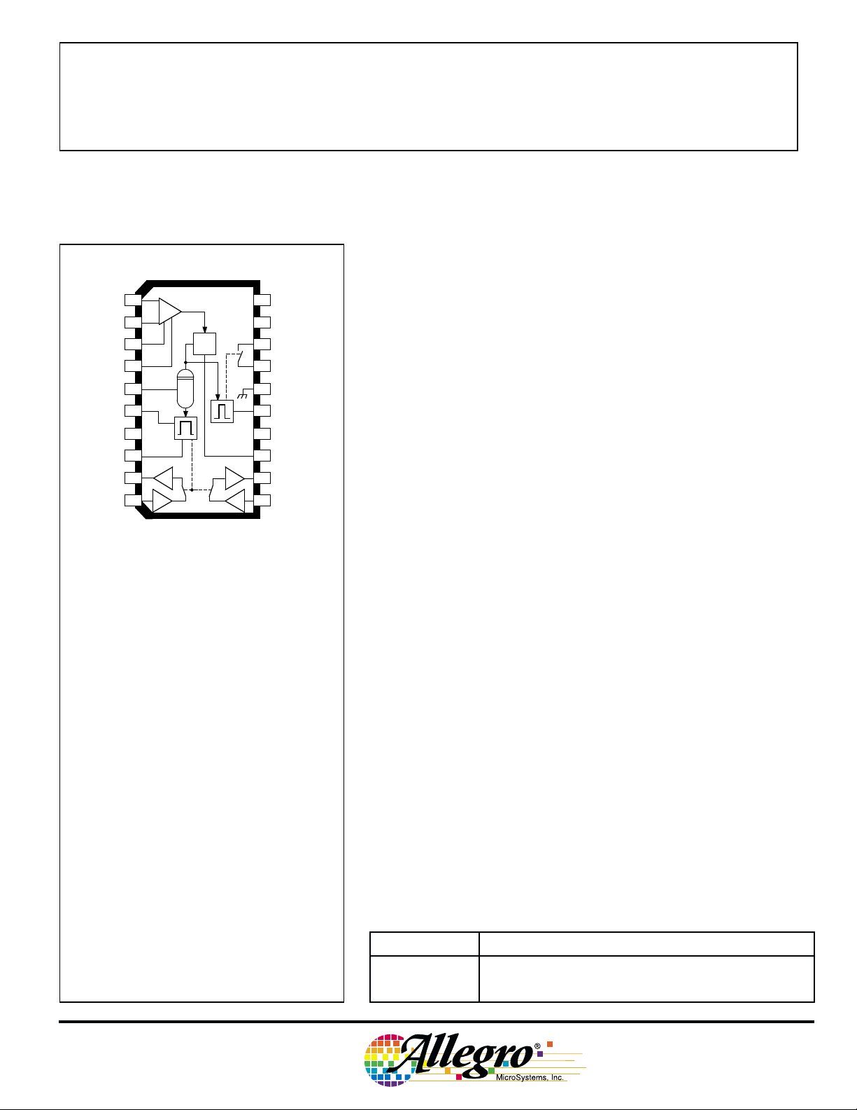
FUNCTIONAL BLOCK DIAGRAM
dV/dt DET
PEAK
DET
13
NOISE
DIFFERENTIATOR
REG
5
69 pF
AUDIO DELAY
6 8
15
RF BLANK TIME
+4 V
100 kΩ
1 kΩ
69 pF
MIXER
100 kΩ
OUT
17
RF GATE
HIGH
40 Ω
18
RF GATE
LOW
AUDIO IN
10
AUDIO OUT
9
AUDIO IN
11
IF
IN
V
CC
1
1
2
NOISE
RF
0.005
60.4 Ω
0.01 0.01
93.1 Ω
187 Ω
AUDIO OUT
AUDIO IN
AUDIO BLANK TIME
1 kΩ
12
AUDIO OUT
2
Dwg. FS-004-1A
TEST CIRCUIT
SUPPLY
267 Ω
V
1
10 µF
+
R
5
R
6
C
8
0.1
2
0.1
3
4
5
6
NC
7
8
9
10
DET
2 kΩ
0.1
1
0.1
1
20
CC
NC
19
R
15
0.001
0.1
RF BYPASS
MIXER OUT
AUDIO OUT
AUDIO IN
Dwg. ES-007-1A
2
2
18
17
16
15
NC
14
13
0.1
12
11
Note that the noise-pulse input is attenuated 20 dB by the test circuit.
115 Northeast Cutoff, Box 15036
Worcester, Massachusetts 01615-0036 (508) 853-5000
Copyright © 1988, 2000 Allegro MicroSystems, Inc.
Page 3

AM NOISE BLANKER
ELECTRICAL CHARACTERISTICS over operating temperature range, at VCC = 7.5 V to
11 V, frf = 1 MHz, Noise (f
) = 500 Hz Square Wave, faf = 1 kHz, Test Figure.
noise
3845
Test
Characteristic Leads Test Conditions Min. Typ. Max. Units
Supply Voltage Range 20 Operating 7.5 9.0 12 V
Quiescent Supply Current 20 VRF = 0 — 15 22 mA
RF INPUT AMPLIFIER:
Trigger Threshold 1 Noise Pulse Amplitude for VRF = 0 45 100 240 µV
Modulation Threshold 1 Noise Pulse Modulation for VRF = 1 mV 35 75 220 %
Detector Rise Time 13 C13 = 0 — 500 — ns
RF SWITCH:
ON Resistance 17-18 — 30 100 Ω
OFF Resistance 17-18 — 100 — kΩ
Time Delay 1-17
AUDIO SWITCHES:
Attenuation 10-9, 11-12 55 80 _ dB
Noise 9, 12 — 1.5 12 mVpp
From Beginning of RF Pulse
to Beginning of RF Blanking
— 1.5 5.0 µs
Limits
Crosstalk 9, 12 40 60 — dB
Gain 10-9, 11-12 -1.2 -0.3 0 dB
Total Harmonic Distortion 9, 12 Vaf =700 mV, V
Input Impedance 10, 11 — 100 — kΩ
Output Impedance 9, 12 — 1.0 — kΩ
BLANKING TIMERS:
RF Blanking 17 R15 = 350 kΩ 35 60 75 µs
Audio Delay 9 R5 = 350 kΩ 30 55 67 µs
Audio Blanking 9 R6 = 110 kΩ, C8 = 0.0012 µF 210 250 400 µs
= 0 — <0.1 1.0 %
noise
www.allegromicro.com
Page 4

3845
AM NOISE BLANKER
CIRCUIT DESCRIPTION
Previous attempts at suppression of impulse
noise in AM receivers have used a variety of
approaches ranging from gating the signal OFF at
the antenna to simply clipping (limiting) any
signal that was larger than the average modulation. Unfortunately, the former can generate as
much noise as it removes while the latter only
reduces the level of noise impulses and does not
remove them.
A major problem in attempting to suppress
impulse noise in an AM receiver can best be
described by looking at the shape of a noise pulse
as it passes through a typical tuner as shown in
the Figure. Here, a typical 0.5 µs pulse is applied
to the antenna input. The resulting waveforms are
essentially the impulse response of the different
selectivity sections as limited only by the dynamic range of the individual sections. Note that
the signal remains quite narrow until the IF filter
is reached. Because of the relatively narrow
bandwidth of the IF filter, the limiting of the IF
amplifier, and the filtering effect of the detector,
the audio output resulting from the impulse is
much wider than the original input pulse and is
therefore much more objectionable.
QUIESCENT DC VOLTAGES
(for circuit design information only)
Typical
Lead Number Function DC Voltage
1 RF In 3.1
2 RF Bypass 3.1
3 RFBias 3.1
4 RF AGC 0.9
5 Audio Delay 4.8
6 Audio Blank Time (R) 4.8
7 No Connection 0
8 Audio BlankTime (C) 4.8
9 Audio Out
10 Audio In
11 Audio In
12 Audio Out
13 Noise Differentiator 4.9
14 No Connection 0
15 RF Blank Time 4.8
16 Ground Reference
17 RF Gate High —
18 RF Gate Low —
19 No Connection 0
20 Supply V
1
1
2
2
4.75
4.0
4.75
4.0
CC
One blanking scheme currently in use senses
the noise pulse in the IF amplifier and blanks the
audio output. This results in a long blanking time
and poor performance at the higher frequencies
where a short blanking time is needed most.
The A3845xLW takes a different approach to
the noise suppression problem by sensing the
noise pulse in the receiver’s RF section and
blanking the pulse before it reaches the IF. This
requires a noise amplifier with a minimum
propagation delay and high-speed gating.
Blanking the noise pulse in this way is very
effective, but some of the interference can still
reach the audio output due to the loss of carrier
during the blanking interval. For this purpose, an
additional delay, blanking interval, and audio
gates are included to further suppress any residual
signal. The result is almost 100% suppression of
impulse noise including that from ignition systems and from sources producing interference at a power line rate such as light dimmers and fluorescent
lamps.
Referring to the Functional Block Diagram, the RF input stage is a
differential amplifier, so that the input impedance is high. The triggering
threshold at the RF amplifier input is about 15 µV at 1 MHz. This means that
a pulsed RF input signal of 15 µV will exceed the threshold and trigger the
blanker. The external capacitor at the dV/dt detector circuit (C13) is selected
so that audio signals do not cause triggering. At high input levels, the
threshold is internally set so that an RF burst of 50% modulation triggers the
blanker. A resistor in parallel with C15 will increase the detection threshold
level.
The RF-switching MOSFET (leads 17-18) is controlled by the RF oneshot whose gate time is determined by the value of R15.
RF Gate Time (µs) = 171 x 10
115 Northeast Cutoff, Box 15036
Worcester, Massachusetts 01615-0036 (508) 853-5000
-12
x R
15
Page 5

TYPICAL PULSE RESPONSE
3845
AM NOISE BLANKER
ANTENNA
BW = "WIDE"
0.5 µs
NOISE
PULSE
RF
20 kHz
50 µs
MIXER
IF
12 kHz
500 µs 600 µs
AUDIO
5 kHz
IF LIMITING
Dwg. OS-001A
The products described here are manufactured
under one or more U.S. patents or U.S. patents
pending.
Allegro MicroSystems, Inc. reserves the right to
make, from time to time, such departures from the
detail specifications as may be required to permit
improvements in the performance, reliability, or
manufacturability of its products. Before placing an
order, the user is cautioned to verify that the information being relied upon is current.
Allegro products are not authorized for use as
critical components in life-support devices or systems
without express written approval.
The information included herein is believed to be
accurate and reliable. However, Allegro
MicroSystems, Inc. assumes no responsibility for its
use; nor for any infringement of patents or other rights
of third parties which may result from its use.
www.allegromicro.com
where R15 should be greater than 33 kΩ. Smaller values for C
will reduce
13
the sensitivity to RF input pulses. The MOSFET turns ON within approximately 1.5 µs (shunting the RF signal to ground) after a noise pulse is
detected and then turns OFF over a 15 µs period after the end of the RF gate
time. The ON resistance of the MOSFET is about 30 Ω. The slow turn-OFF
prevents any additional transients from being introduced into the receiver by
the RF gate. The internal gate circuit also includes charge-balancing circuits
so that switching transients are canceled and do not appear at the output.
These features ensure transient-free switching even when the RF gate is
connected to the low-level input stages of a receiver. Note that the RF gate
must be connected to a supply to obtain the minimum ON-resistance of the
MOSFET gate. This makes it convenient to connect the RF gate in parallel
with the receiver mixer output transformer primary.
Blanking in the RF or mixer sections of the receiver removes most of the
noise pulse but a small amount still remains due to the hole punched in the
carrier. This residual noise is theoretically somewhere between the peak
audio and 100% negative modulation but is significantly smaller and narrower
than that which the impulse would normally produce without blanking. An
audio delay, one-shot, and audio gates are included to eliminate this residual
signal.
Page 6

3845
AM NOISE BLANKER
The audio delay is determined by the value of
R5:
Audio Gate Delay (µs) = 157 x 10
where R5 should be greater than 33 kΩ. The
amount of delay required will depend on the IF
filtering characteristics of the particular receiver
design. After the audio delay time, the audio oneshot is triggered. The audio switching MOSFETs
(leads 9-10 and leads11-12) are controlled by the
audio one-shot whose gate time is determined by
the values of R6 and C8:
Audio Gate Time (µs) = 1.9 x R6 x C
The MOSFET audio gates also include
charge-balancing circuits to eliminate switching
transients.
-12
x R
5
8
TYPICAL APPLICATION
A typical application uses the A3845xLW in a C-QUAM® AM stereo
car-radio tuner with its input from between the RF tuned circuits and the
mixer input. Although there is a 1.5 µs delay from the beginning of the noise
pulse to the start of blanking, this is small compared with the impulse response time of the receiver. It takes almost 10 µs for the RF noise burst to
reach 70% amplitude at the mixer input. The blanker RF input could be
connected to the collector of the discrete RF amplifier, but the bandwidth is
much wider there and false triggering from strong adjacent channel signals
could occur.
The A3845xLW noise blanker can also be used in dual-conversion AM
tuners. The blanker RF input would then be connected at the first IF amplifier
input and the blanker RF gate connected at the second mixer output. Because
the first IF band-width is usually relatively wide, the noise pulses are narrower, and the RF blanking time will be correspondingly less. In this case, it
may be necessary to reduce the value of capacitor C13 so that the noise
separator does not extend the RF blanking time.
TYPICAL RF FREQUENCY
RESPONSE
0
-5
-10
RELATIVE SENSITIVITY IN dB
-15
COIL INFORMATION FOR HIGH-PERFORMANCE ETR
AM STEREO RECEIVER WITH
NOISE BLANKING
Symbol Q N1:N2 N1:N3 Toko Part Number
Antenna T
RF T2, T
Local Osc. T
Mixer T
Detector L
1
120 10:1 RWOS-6A7894AO,
3
4
5
2
120 5:1 7TRS-A5609AO
100 A7BRS-T1041Z,
® Registered trademark of MOTOROLA, INC.
1:1.6 7HN-60064CY
L = 178 µH
2:1 8.9:1 7LC-502112N4,
CT = 180 pF
C
= 1000 pF
T
0.1 1.0 10
RF INPUT FREQUENCY IN MHz
Dwg. GS-006
115 Northeast Cutoff, Box 15036
Worcester, Massachusetts 01615-0036 (508) 853-5000
Page 7

3845
AM NOISE BLANKER
ETR AM-STEREO RECEIVER WITH NOISE BLANKING
www.allegromicro.com
Page 8

3845
AM NOISE BLANKER
20 11
Dimensions in Inches
(for reference only)
0.0125
0.0091
0.2992
0.2914
0.020
0.013
0.0926
0.1043
7.60
7.40
1 2
0.0040
20
MIN.
3
0.050
0.5118
0.4961
BSC
Dimensions in Millimeters
(controlling dimensions)
11
0.419
0.394
0.050
0.016
0° TO 8°
Dwg. MA-008-20 in
0.32
0.23
10.65
10.00
1.27
0.40
0.51
0.33
2.65
2.35
1
0.10
2
MIN.
3
13.00
12.60
1.27
BSC
NOTES: 1. Exact body and lead configuration at vendor’s option within limits shown.
2. Lead spacing tolerance is non-cumulative.
3. Supplied in standard sticks/tubes of 37 devices or add “TR” to part number for tape and reel.
115 Northeast Cutoff, Box 15036
Worcester, Massachusetts 01615-0036 (508) 853-5000
0° TO 8°
Dwg. MA-008-20 mm
 Loading...