

Page 1
The A3425LK dual Hall-effect switch is an extremely
temperature-stable and stress-resistant sensor especially suited for use in
digital-encoder systems in the harsh environments of automotive or
industrial applications over extended temperature ranges to +150°C.
Superior high-temperature performance is made possible through
dynamic offset cancellation, which reduces the residual offset voltage
normally caused by device overmolding, temperature dependencies, and
thermal stress. This device also eliminates the major manufacturing
hurdles encountered in fine-pitch direction-detection applications,
namely maintaining accurate mechanical location between the two active
Hall elements. Here, the two Hall elements are photolithographically
aligned to better than 1 µm, as contrasted with 100 µm or worse mechanical location tolerance when manufactured discretely. The
A3425LK is an ultra-sensitive device optimized for use with highdensity ring magnets.
The device includes on a single silicon chip a voltage regulator, two
independent chopper-stabilized Hall-voltage generators , two smallsignal amplifiers, two Schmitt triggers, and two short-circuit protected
open-collector outputs to sink up to 30 mA each. An on-board regulator
permits operation with supply voltages of 3.3 to 26.5 volts. With
suitable output pull ups, it can be used directly with bipolar or MOS
logic circuits.
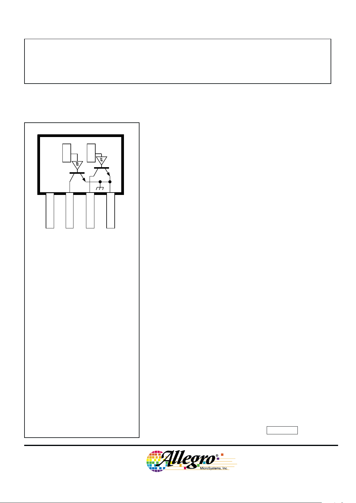
The A3425LK dual Hall-effect switch is supplied in a 4-pin plastic
SIP for operation over a temperature range of -40°C to +150°C. A
similar device, with on-chip logic processing specifically for direction
detection applications, in a 5-pin SIP, is the A3422LKA.
FEATURES
■ Two Matched Hall Switches On A Single Substrate
■ 1 mm Sensor-to-Sensor Spacing
■ Superior Temperature Stability
■ Resistant to Physical Stress
■ Output Short-Circuit Protection
■ Operation From Unregulated Supply
■ Reverse Battery Protection
■ Solid-State Reliability
■ Integrated ESD Protection on Outputs and Supply
Data Sheet
27651.20
PRELIMINARY INFORMATION
(subject to change without notice)
August 21, 2000
Pinning is shown viewed from branded side.
DUAL, CHOPPER-STABILIZED, ULTRA-SENSITIVE,
BIPOLAR HALL-EFFECT SWITCH
3425
ABSOLUTE MAXIMUM RATINGS
at TA = +25°C
Supply Voltage, VCC........................ 26.5 V
Reverse Battery Voltage, V
RCC
.......... -18 V
Zener Current, IZ............................ 100 mA
Magnetic Flux Density, B ........... Unlimited
Output Off Voltage, V
OUT
.................... V
CC
Output Current, I
OUT
........................ 30 mA
Reverse Output Current, I
OUT
........ -50 mA
Package Power Dissipation, PD. See Graph
Junction Temperature, TJ............... +170°C
Operating Temperature Range,
TA, ............................ -40°C to +150°C
Storage Temperature Range,
TS.............................. -65°C to +170°C
Always order by complete part number, e.g., A3425LK .
Dwg. PH-017
1
SUPPLY
V
CC
4
GROUND
32
X
OUTPUT
2
OUTPUT
1
X
Page 2
3425
DUAL, CHOPPER-STABILIZED,
ULTRA-SENSITIVE,
BIPOLAR HALL-EFFECT SWITCH
115 Northeast Cutoff, Box 15036
Worcester, Massachusetts 01615-0036 (508) 853-5000
2
FUNCTIONAL BLOCK DIAGRAM
Copyright © 2000, Allegro MicroSystems, Inc.
OUTPUT
1
<1Ω
X
DYNAMIC
OFFSET CANCELLATION
REG.
TO ALL
SUBCIRCUITS
SUPPLY
CONTROL
CURRENT
LIMIT
SAMPLE
& HOLD
LOW-PASS
FILTER
Dwg. FH-020-7
GROUND
OUTPUT
2
<1Ω
X
DYNAMIC
OFFSET CANCELLATION
CONTROL
CURRENT
LIMIT
SAMPLE
& HOLD
LOW-PASS
FILTER
1
2
3
4
E1
E2
75 100 125 150 175
1.0
0.2
0
ALLOWABLE PACKAGE POWER DISSIPATION IN WATTS
AMBIENT TEMPERATURE IN °C
0.8
0.6
0.4
50
Dwg. GH-001-1
250
FREE AIR, R = 177°C/W
θJA
-25
Page 3

3425
DUAL, CHOPPER-STABILIZED,
ULTRA-SENSITIVE,
BIPOLAR HALL-EFFECT SWITCH
www.allegromicro.com
3
ELECTRICAL CHARACTERISTICS over operating temperature range, each switch tested
separately (unless otherwise specified).
Limits
Characteristic Symbol Test Conditions Min. Typ. Max. Units
Supply Voltage Range V
CC
Operating, TJ < 170°C
1
3.3 – 26.5 V
Output Leakage Current I
OFF
V
OUT
= 18 V, B < B
RP
– <1.0 10 µA
Output Saturation Voltage V
OUT(SAT)
I
OUT
= 20 mA, B > B
OP
– 225 400 mV
Output Current Limit I
OM
B > B
OP
30 – 55 mA
Chopping Frequency f
C
– 340 – kHz
Output Rise Time t
r
RL = 820 Ω, CL = 10 pF – 110 – ns
Output Fall Time t
f
RL = 820 Ω, CL = 10 pF – 55 – ns
Total Supply Current I
CC
Both outputs off, VCC ≤ 26.5 V – 3.8 6.0 mA
Both outputs on, VCC ≤ 26.5 V – 7.5 10 mA
Reverse Battery Current I
CC
V
RCC
= -18 V – 2.0 15 mA
Zener Voltage VZ + V
D
ICC = 15 mA, TA = 25°C 283337 V
Zener Impedance zz + z
D
ICC = 15 mA, TA = 25°C – 50 100 Ω
NOTES:1. Supply voltage is limited by allowable package power dissipation as a function of ambient temperature.
2. BOP = operate point (output turns on); BRP = release point (output turns off).
3. Typical Data is at TA = +25°C and VCC = 12 V and is for design information only.
MAGNETIC CHARACTERISTICS over operating supply voltage and temperature ranges, each
switch tested separately (unless otherwise specified).
Limits
Characteristic Symbol Test Conditions Min. Typ. Max. Units
Operate Point B
OP1
– 8.0 24 G
B
OP2
–1124G
Release Point B
RP1
-24 -11 – G
B
RP2
-24 -8.0 – G
Hysteresis B
hys
BOP – B
RP
5.0 19 35 G
Operate Differential B
OP(dif)
B
OP1
– B
OP2
– -2.0 ±30 G
Release Differential B
RP(dif)
B
RP1
– B
RP2
– -3.3 ±30 G
Symmetry B
sym
BOP + B
RP
––±30 G
NOTES:1. As used here, negative flux densities are defined as less than zero (algebraic convention) and -50 G is less than +10 G.
2. Typical Data is at TA = +25°C and VCC = 12 V and is for design information only.
Page 4
3425
DUAL, CHOPPER-STABILIZED,
ULTRA-SENSITIVE,
BIPOLAR HALL-EFFECT SWITCH
115 Northeast Cutoff, Box 15036
Worcester, Massachusetts 01615-0036 (508) 853-5000
4
TYPICAL OPERATING CHARACTERISTICS
as a function of temperature
TOTAL SUPPLY CURRENT
OUTPUT SATURATION VOLTAGE
CHANNEL 2 SWITCH POINTS
0 50 100
AMBIENT TEMPERATURE IN °C
-50
Dwg. GH-026-7
SWITCH POINT IN GAUSS
0
5
150-25 25 75 125
10
15
20
25
-25
-20
-15
-10
-5
RELEASE POINT
VCC = 18-26.5 V
V
CC
= 3.3-5 V
VCC = 5 V
V
CC
= 3.3 V
V
CC
= 18 V
V
CC
= 26.5 V
OPERATE POINT
0 50 100
AMBIENT TEMPERATURE IN °C
-50
Dwg. GH-026-8
SWITCH POINT IN GAUSS
0
5
OPERATE POINT
150-25 25 75 125
10
15
20
25
-25
-20
-15
-10
-5
RELEASE POINT
VCC = 26.5 V
V
CC = 18 V
V
CC = 3.3-5 V
VCC = 26.5 V
V
CC = 5 V
V
CC = 18 V
V
CC = 3.3 V
CHANNEL 1 SWITCH POINTS
0 25 50 75 100
300
0
AMBIENT TEMPERATURE IN °C
200
100
-50
Dwg. GH-029-5
SATURATION VOLTAGE IN mV
150-25 125
I
OUT
= 20 mA
VCC = 26.5 V
VCC = 3.3 V
0
SUPPLY CURRENT IN mA
8
6
4
2
0 255075100
AMBIENT TEMPERATURE IN °C
-50
Dwg. GH-028-8
125-25 150
B ≥ B
OP
VCC = 18 V
VCC = 18 V
VCC = 3.3 V
VCC = 3.3 V
B ≤ B
RP
Page 5

3425
DUAL, CHOPPER-STABILIZED,
ULTRA-SENSITIVE,
BIPOLAR HALL-EFFECT SWITCH
www.allegromicro.com
5
SENSOR LOCATIONS
(±0.005" [0.13 mm] die placement)
Although sensor location is accurate to three sigma for a
particular design, product improvements may result in small
changes to sensor location.
A
1 432
Dwg. MH-001-4
0.015"
0.38 mm
NOM
0.053"
1.34 mm
BRANDED
SURFACE
ACTIVE AREA DEPTH
0.083"
2.11 mm
0.039"
1.00 mm
E1 E2
Allegro
TYPICAL OPERATING CHARACTERISTICS (cont'd)
as a function of supply voltage
OPERATE AND RELEASE DIFFERENTIALS
0 50 100
AMBIENT TEMPERATURE IN °C
-50
Dwg. GH-026-9
B
OP
/B
RP
DIFFERENTIAL IN GAUSS
0
5
150-25 25 75 125
10
15
20
25
-25
-20
-15
-10
-5
BOP
V
CC
= 3.3 V
V
CC
= 5-18 V
BRP
V
CC
= 3.3 V
V
CC
= 5 V
V
CC
= 18 V
Page 6

3425
DUAL, CHOPPER-STABILIZED,
ULTRA-SENSITIVE,
BIPOLAR HALL-EFFECT SWITCH
115 Northeast Cutoff, Box 15036
Worcester, Massachusetts 01615-0036 (508) 853-5000
6
CRITERIA FOR DEVICE QUALIFICATION
Qualification Test Test Method and Test Conditions Test Length Samples Comments
Biased Humidity (HAST) JESD22-A101, 1000 hrs 77 VCC = V
OUT
= 3.3 V
TA = 85°C, RH = 85%
High-Temperature JESD22-A108, 1000 hrs 77
Operating Life (HTOL) TA = 150°C, TJ = 165°C
Accelerated HTOL TA = 170°C, TJ = 180°C 168 hrs 77
Autoclave, Unbiased JESD22-A102, Condition C, 96 hrs 77
High-Temperature MIL-STD-883, Method 1008, 1000 hrs 77
(Bake) Storage Life TA = 170°C
Temperature Cycle MIL-STD-883, Method 1010, 1000 cycles 77
-55°C to +150°C
ESD, CDF-AEC-Q100-002 Pre/Post x per Test to failure,
Human Body Model Reading test All leads > TBD
All Allegro sensors are subjected to stringent qualification requirements prior to being released to production.
To become qualified, except for the destructive ESD tests, no failures are permitted.
Page 7

3425
DUAL, CHOPPER-STABILIZED,
ULTRA-SENSITIVE,
BIPOLAR HALL-EFFECT SWITCH
www.allegromicro.com
7
FUNCTIONAL DESCRIPTION
Chopper-Stabilized Technique. These devices use a
proprietary dynamic offset cancellation technique, with an
internal high-frequency clock to reduce the residual offset
voltage of the Hall element that is normally caused by
device overmolding, temperature dependencies, and
thermal stress. This technique produces devices that have
an extremely stable quiescent Hall output voltage, are
immune to thermal stress, and have precise recoverability
after temperature cycling. This technique will also
slightly degrade the device output repeatability.
The Hall element can be considered as a resistor array
similar to a Wheatstone bridge. A large portion of the
offset is a result of the mismatching of these resistors.
The chopper-stabilizing technique cancels the mismatching of the resistors by changing the direction of the current
flowing through the Hall plate and Hall voltage measurement taps, while maintaining the Hall-voltage signal that
is induced by the external magnetic flux. The signal is,
then, captured by a sample-and-hold circuit.
More detailed descriptions of the circuit operation can
be found in: Technical Paper STP 97-10, Monolithic
Magnetic Hall Sensor Using Dynamic Quadrature Offset
Cancellation and Technical Paper STP 99-1, ChopperStabilized Amplifiers With A Track-and-Hold Signal
Demodulator.
Operation. The output of these devices switches low
(turns on) when a magnetic field perpendicular to the Hall
sensor exceeds the operate point threshold (B
OP
). After
turn-on, the output is capable of sinking 30 mA and the
output voltage is V
OUT(SAT)
. When the magnetic field is
reduced below the release point (B
RP
), the device output
switches high (turns off). Note especially that release can
occur when the magnetic field is removed but to ensure
release, a field reversal is required. The difference in the
magnetic operate and release points is the hysteresis (B
hys
)
of the device. This built-in hysteresis allows clean
switching of the output even in the presence of external
mechanical vibration and electrical noise.
Dwg. EH-012
REG
SAMPLE
& HOLD
X
+V
HALL
VOLTAGE
B
+
—
Dwg. AH-011-2
0 +B
0
OUTPUT VOLTAGE
FLUX DENSITY
Dwg. GH-034-5
-B
RP
B
V
OUT(SAT)
CC
V
OP
B
+V
Page 8

3425
DUAL, CHOPPER-STABILIZED,
ULTRA-SENSITIVE,
BIPOLAR HALL-EFFECT SWITCH
115 Northeast Cutoff, Box 15036
Worcester, Massachusetts 01615-0036 (508) 853-5000
8
Quadrature/Direction Detection. External logic
circuitry can be used to determine the direction of movement of the magnetic field across the face of the package.
For the direction signal to be appropriately updated, a
quadrature relationship must be maintained between the
ring magnet pole width*, the sensor-to-sensor spacing,
and, to a lesser extent, the magnetic switch points. For
optimal design, the sensor should be actuated with a ring
magnet pole width* two times the sensor-to-sensor
spacing. This will produce a sinusoidal magnetic field
whose period (denoted as
Τ
) is then four times the sensorto-sensor spacing. A quadrature relationship can also be
maintained for a ring magnet that has a period that satisfies the relationship n
Τ
/4 = 1.0 mm, where n is any odd
integer. Therefore, ring magnets with pole-pair spacings
equal to 4 mm (n = 1), 1.3 mm (n = 3), etc. are permitted.
The response of the device to the magnetic field
produced by a rotating ring magnet is shown above. Note
the desired phase shift between the two integrated sensors.
* “Pole” refers to a single pole (North or South)
unless stated as “pole pair” (North
and South).
BOP1
BRP1
Dwg. WH-012-1
+B
-B
+B
-B
BRP2
OUTE1
OUTE2
BOP2
APPLICATIONS INFORMATION
Over-Current Protection. Current through each output
transistor is sensed with a low-value (<1 Ω) on-chip
aluminum resistor. The voltage drop across this resistor is
fed back to control the base drive of that output. This
feedback prevents the output transistor from exceeding its
maximum current-density rating by limiting the output
current to between 30 mA and 55 mA. In this mode, the
device will come out of saturation and dissipate an increased amount of power
P
D
= V
OUT
x I
OM
where V
OUT
= VCC - (IOM x RL)
and the output transistor will be thermally stressed. This
stress, unless protected against, will cause the device
junction temperature to rise until it fails catastrophically.
Over-current limiting is intended to protect the device
from transient overloads and should not imply that output
short circuits are permitted.
Page 9

3425
DUAL, CHOPPER-STABILIZED,
ULTRA-SENSITIVE,
BIPOLAR HALL-EFFECT SWITCH
www.allegromicro.com
9
Rotated sensor for
fine-pitch ring
magnets
A
12 43
Dwg. MH-024-1
α
TARGET FACE WIDTH, F
>1.00 SIN α (mm)
>0.039 SIN
α
(inch)
1.00 COS
α
(mm)
0.039 COS
α
(inch)
0.039"
1.00 mm
A
1
2
4
3
APPLICATIONS INFORMATION (cont'd)
Power Dissipation and Junction Temperature.
Operating characteristics are limited by allowable package
power dissipation (P
D
) as a function of ambient tempera-
ture (T
A
), which is defined by the maximum internal
junction temperature (T
J
= 170°C) and the package
thermal resistance (R
θJA
= 177°C/W).
P
D
= (TJ – TA)/R
θJA
= (170 – TA)/177
This is shown in the graph on page 2.
Actual or required package power dissipation is the
sum of the two output powers (d.c. x I
OUT1
x V
OUT(SAT)1
) +
(d.c. x I
OUT2
x V
OUT(SAT)2
) and the sensor power (ICC x
V
CC
).
At high ambient operating temperatures (above about
120°C), it is easy to exceed the allowable package power
dissipation. In this case, the output currents or the supply
voltage must be reduced.
Operation with Fine-Pitch Ring Magnets. For
targets with a circular pitch of less than 4 mm, a performance improvement can be observed by rotating the front
face of the sensor subassembly (see below). This sensor
rotation decreases the effective sensor-to-sensor spacing,
provided that the Hall elements are not rotated beyond the
width of the target.
Applications. It is strongly recommended that an
external 0.01 µF bypass capacitor be connected (in close
proximity to the Hall sensor) between the supply and
ground of the device to reduce both external noise and
noise generated by the internal logic.
The simplest form of magnet that will operate these
devices is a ring magnet. Other methods of operation,
such as linear magnets, are possible. Extensive applications information on magnets and Hall-effect sensors is
also available in the “Hall-Effect IC Applications Guide”
which can be found in the latest issue of the Allegro
MicroSystems Electronic Data Book, AMS-702 or Application Note 27701, or at
www.allegromicro.com
Page 10

3425
DUAL, CHOPPER-STABILIZED,
ULTRA-SENSITIVE,
BIPOLAR HALL-EFFECT SWITCH
115 Northeast Cutoff, Box 15036
Worcester, Massachusetts 01615-0036 (508) 853-5000
10
Dimensions in Inches
(controlling dimensions)
Dimensions in Millimeters
(for reference only)
NOTES: 1. Tolerances on package height and width represent allowable mold offsets. Dimensions given are measured at the widest point
(parting line).
2. Exact body and lead configuration at vendor’s option within limits shown.
3. Height does not include mold gate flash.
4. Recommended minimum PWB hole diameter to clear transition area is 0.035" (0.89 mm).
5. Where no tolerance is specified, dimension is nominal.
SURFACE-MOUNT LEAD FORM (order A3425LK-TL)
2.41
±0.13
0.51
MIN
FLAT
Dwg. MH-015 mm
0.10
MAX
0.051
MAX
0°–8°
0.095
±0.005
0.020
MIN
FLAT
Dwg. MH-015 in
0.004
MAX
0.002
MAX
0°–8°
45°
Dwg. MH-009D in
0.063
0.059
0.033
0.0173
0.0138
0.0189
0.0142
0.050
BSC
1234
45°
SEE NOTE
0.208
0.203
0.138
0.133
0.600
0.560
0.085
MAX
45°
Dwg. MH-009D mm
1.60
1.50
0.84
0.44
0.35
0.48
0.36
1.27
BSC
1234
45°
SEE NOTE
5.28
5.16
3.51
3.38
15.24
14.23
2.16
MAX
Page 11

3425
DUAL, CHOPPER-STABILIZED,
ULTRA-SENSITIVE,
BIPOLAR HALL-EFFECT SWITCH
www.allegromicro.com
11
This page is intentionally left blank.
Page 12

3425
DUAL, CHOPPER-STABILIZED,
ULTRA-SENSITIVE,
BIPOLAR HALL-EFFECT SWITCH
115 Northeast Cutoff, Box 15036
Worcester, Massachusetts 01615-0036 (508) 853-5000
12
The products described herein are manufactured under one or
more of the following U.S. patents: 5,045,920; 5,264,783; 5,442,283;
5,389,889; 5,581,179; 5,517,112; 5,619,137; 5,621,319; 5,650,719;
5,686,894; 5,694,038; 5,729,130; 5,917,320; and other patents
pending.
Allegro MicroSystems, Inc. reserves the right to make, from time to
time, such departures from the detail specifications as may be
required to permit improvements in the performance, reliability, or
manufacturability of its products. Before placing an order, the user is
cautioned to verify that the information being relied upon is current.
Allegro products are not authorized for use as critical components
in life-support appliances, devices, or systems without express written
approval.
The information included herein is believed to be accurate and
reliable. However, Allegro MicroSystems, Inc. assumes no responsibility for its use; nor for any infringements of patents or other rights of
third parties that may result from its use.
HALL-EFFECT SENSORS
Partial Part Avail. Oper. Characteristics at TA = +25°C
Number Temp. B
OP
max B
RP
min B
hys
typ Features Notes
GEARTOOTH/RING MAGNET (DUAL ELEMENT) HALL-EFFECT SENSORS in order of B
OP
3060 K/S +35 -35 30 ac coupled
3422 E/L +75 -75 46 direction detection
3059 K/S +100 -100 130 ac coupled
3056 E/L +150 -150 50 zero-speed
3058 E/L +250 -250 200 zero-speed
3421 E/L +280 -280 335 direction detection
SPECIAL-PURPOSE HALL-EFFECT SENSORS
3054 K/S +300 +5.0 50 unipolar switch, multiplexed 6
3209 E ±60 ±5.0 7.7 400 µW, chopper stabilized
3210 E ±60 ±5.0 7.7 25 µW, chopper stabilized
3421 E/L +280 -280 335 direction detection
3422 E/L +85 -85 46 direction detection
3425 L +24 -24 19 dual, chopper stabilized 1
Operating Temperature Ranges:
S = -20°C to +85°C, E = -40°C to +85°C, J = -40°C to +115°C, K = -40°C to +125°C, L = -40°C to +150°C
Notes 1. Protected.
6. Multiplexed two-wire sensor; after proper address, power/signal bus current indicates magnetic field condition.
 Loading...