

Page 1
Always order by complete part number, e.g., A3197LU .
3197
PROTECTED, HIGH-TEMPERATURE,
OPEN-COLLECTOR HALL-EFFECT LATCH
These open-collector Hall-effect latches are capable of sensing magnetic
fields while using an unprotected power supply. The A3197LLT and A3197LU
can provide position and speed information by providing a digital output for
magnetic fields that exceed their predefined switch points. These devices
operate down to zero speed and have switch points that are designed to be
extremely stable over a wide operating temperature and voltage range. The
latching characteristics make them ideal for use in pulse counting applications
when used with a multi-pole ring magnet. Thermal and output short-circuit
protection allow an increased wiring harness fault tolerance. The temperature
compensated switch points, the wide operating voltage range, and the integrated
protection make these devices ideal for use in automotive applications such as
transmission speed sensors and integrated wheel bearing speed sensors.
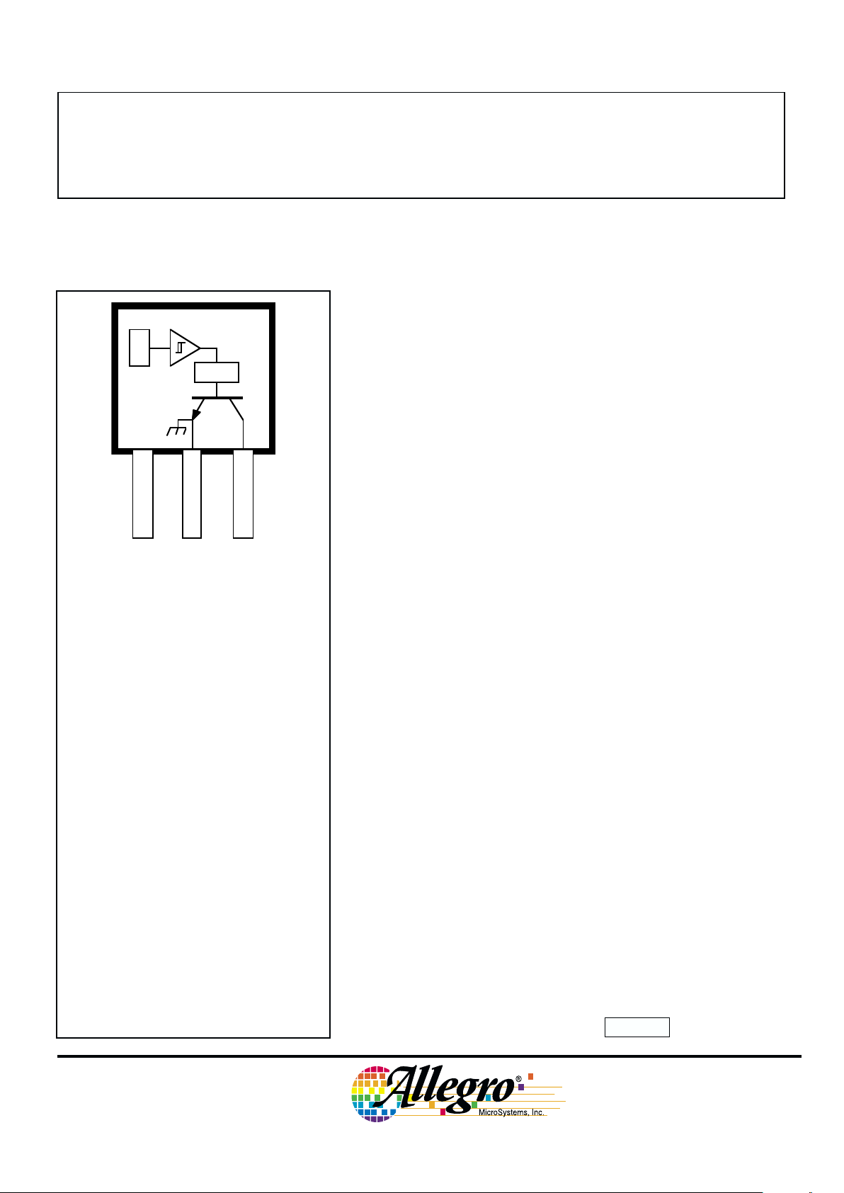
Each monolithic device contains an integrated Hall-effect transducer, a
temperature-compensated comparator, a voltage regulator, and a buffered 35 mA
output sink stage. Supply protection is made possible by the integration of
overvoltage and undervoltage shutdown circuitry that monitor supply fault
conditions and shut down the IC. Noise shutdown circuitry (patent applied for)
prevents the propagation of supply transients to the logic load. Output protection circuitry includes a current limit loop that limits the maximum output sink
current, and thermal protection circuitry that shuts down the device during an
over-heating condition such as with a shorted load.
The A3197LLT and A3197LU are rated for operation over an extended
temperature range of -40°C to +150°C. They are supplied in a three-lead SIP
(suffix ‘U’) or a surface-mount SOT-89 (suffix ‘LT’).
FEATURES
■ Internal Protection For Automotive (ISO/DIN) Transients
■ Operation From Unregulated Supply
■ Reverse Battery Protection
■ Undervoltage Lockout
■ Supply Noise-Suppression Circuitry
■ Output Short-Circuit Protection
■ Output Zener Clamp
■ Thermal Protection
■ Symmetrical Latching Switch Points
■ Operable with Multipole Ring Magnets
Data Sheet
27609.10A
ABSOLUTE MAXIMUM RATINGS
Supply Voltage, V
CC
(100 ms) ................................... 115 V*
(continuous) ............................... 28 V*
Reverse Battery Voltage, V
RCC
(100 ms) ................................... -100 V
(continuous) ............................... -35 V
Magnetic Flux Density, B .......... Unlimited
Output OFF Voltage, V
OUT
................. 26 V
Reverse Output Voltage V
OUT
......... -0.5 V
Continuous Output Current,
I
OUT
.......................................... 35 mA*
Reverse Output Current,
I
OUT
........................................ -100 mA
Package Power Dissipation,
PD....................................... See Graph
Junction Temperature, TJ................. 170°C
Operating Temperature Range,
T
A
..........................................
-40°C to +150°C
Storage Temperature, TS.................. 170°C
*Fault condition, internal overvoltage shutdown
above 28 V; output current limited above 35 mA.
Dwg. PH-003-2
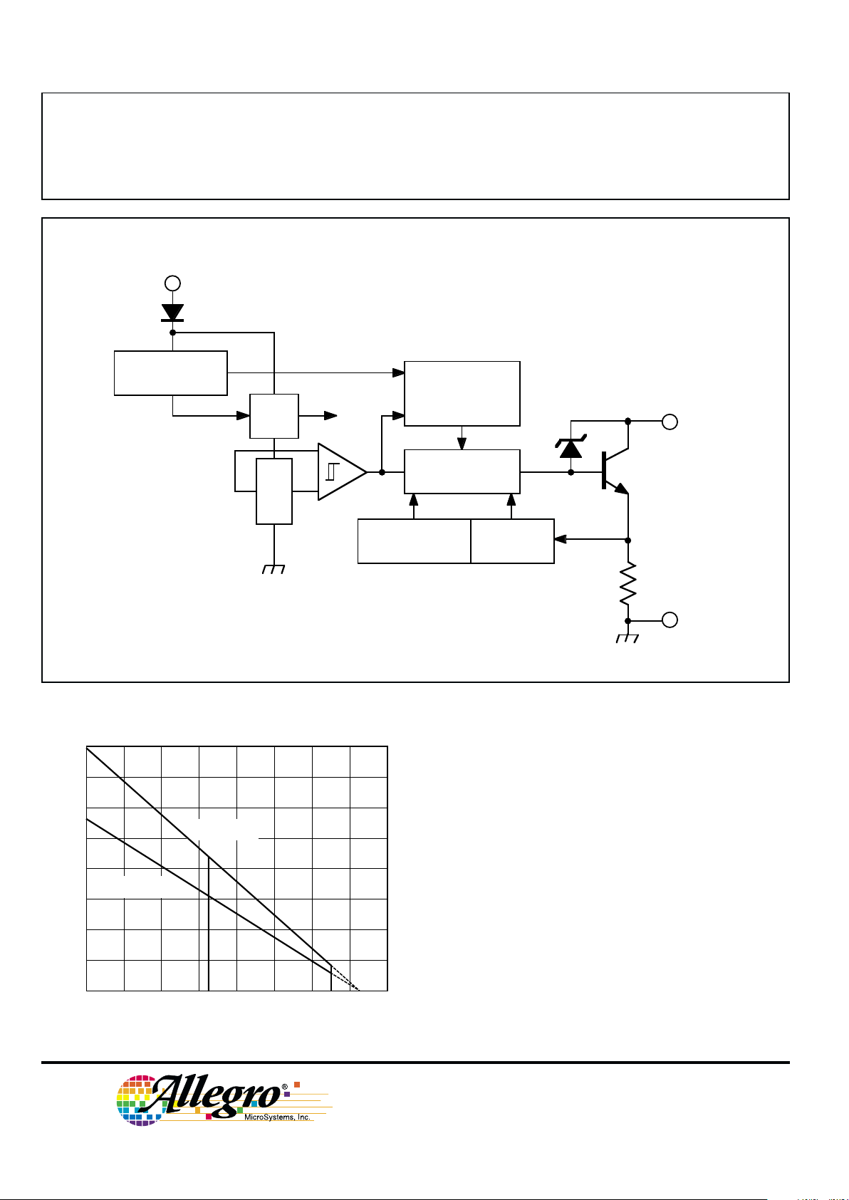
1
SUPPLY
V
CC
GROUND
32
OUTPUT
X
PTCT
Page 2
3197
PROTECTED, HIGH-TEMP.,
OPEN-COLLECTOR
HALL-EFFECT LATCH
115 Northeast Cutoff, Box 15036
Worcester, Massachusetts 01615-0036 (508) 853-5000
FUNCTIONAL BLOCK DIAGRAM
REG.
OUTPUT
3
X
Dwg. FH-012A
GROUND
V
CC
1
<1Ω
POWER UP &
TRANSIENT
PROTECTION
CURRENT
LIMIT
2
OVERVOLT.
LOCKOUT
THERMAL
SHUTDOWN
CONTROL
600
400
200
40 80 120
160
0
AMBIENT TEMPERATURE IN °C
ALLOWABLE PACKAGE POWER DISSIPATION IN mW
Dwg. GH-054A
"U" PACKAGE
R
θJA
= 183°C/W
"LT" PACKAGE
R
θJA
= 258°C/W
60 100 140 180
700
500
300
100
20
800
NOTE – Permitted duty cycle will be less than 100%
at maximum ambient temperature with high supply
voltages, i.e., TA ≥ 140°C, VCC ≥ 12 V, and the “LT”
package. The thermal shutdown circuitry does not
protect the device from these stresses (see Internal
Protective Features).
Copyright © 1995, 1999, Allegro MicroSystems, Inc.
Page 3
3197
PROTECTED, HIGH-TEMP.,
OPEN-COLLECTOR
HALL-EFFECT LATCH
www.allegromicro.com
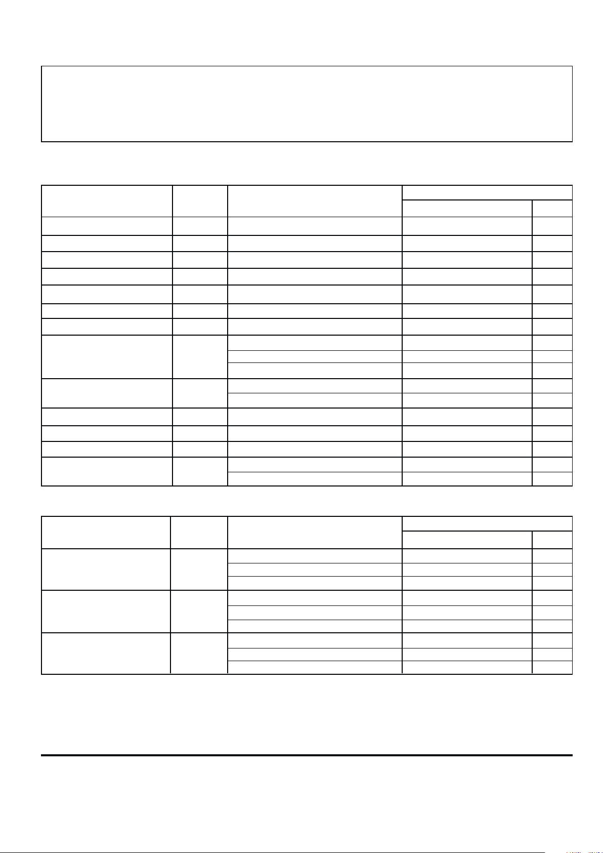
Limits
Characteristic Symbol Test Conditions Min. Typ. Max. Units
Operate Point B
OP
TA = -40°C 60 130 200 G
T
A
= +25°C 50 110 160 G
TA = +150°C 40 105 150 G
Release Point B
RP
TA = -40°C -200 -140 -60 G
TA = +25°C -160 -120 -50 G
TA = +150°C -150 -100 -40 G
Hysteresis B
hys
TA = -40°C 150 270 — G
(BOP - BRP)T
A
= +25°C 130 230 — G
T
A
= +150°C 110 205 — G
ELECTRICAL CHARACTERISTICS
over operating voltage and temperature range
(unless otherwise specified).
MAGNETIC CHARACTERISTICS over operating voltage range
(unless otherwise specified).
NOTES:BOP = magnetic operate point (output turns ON); BRP = magnetic release point (output turns OFF).
As used here, negative flux densities are defined as less than zero (algebraic convention).
Typical values are at TA = +25°C and VCC = 12 V (unless otherwise specified).
* Fault condition. Device is shut down and operation is not possible.
Limits
Characteristic Symbol Test Conditions Min. Typ. Max. Units
Supply Voltage V
CC
Operating (but VCC x ICC vs TA limited) V
CC(UV)
12 26 V
Overvoltage Shutdown* V
CC(OV)
B > B
OP
28 — 55 V
Undervoltage Shutdown* V
CC(UV)
B > B
OP
3.7 — 4.5 V
Output Voltage, On V
OUT(SAT)
B > B
OP, IOUT
= 30 mA, VCC = 16 V — 0.2 0.5 V
Output Leakage Current I
OFF
V
OUT
= 26 V — — 5.0 µA
Output Clamp Voltage V
OUT(CLMP)
B < BRP, VCC = 115 V*, I
OUT
= 0 28 32 40 V
Output Current Limit I
OUTMAX
B > BOP, V
OUT
= 12 V 355070mA
Supply Current I
CC
B < BRP, VCC = 24 V, I
OUT
= 0 — 5.2 9.0 mA
B > BOP, VCC = 24 V, I
OUT
= 20 mA — 7.8 12 mA
V
CC
= +115 V* — 8.0 17 mA
Reverse Battery Current* I
RCC
V
RCC
= -35 V* — -0.5 -5.0 mA
V
RCC
= -100 V* — -2.0 -10 mA
Output Rise Time t
r
CL = 20 pF, RL = 330 Ω, VBB = 12 V — 0.05 2.0 µs
Output Fall Time t
f
CL = 20 pF, RL = 330 Ω, VBB = 12 V — 0.30 5.0 µs
Thermal Shutdown Temp.* T
J
165 — 190 °C
Package Thermal Resist. R
θJA
“LT” Package — 258 — °C/W
“U” Package — 183 — °C/W
Page 4
3197
PROTECTED, HIGH-TEMP.,
OPEN-COLLECTOR
HALL-EFFECT LATCH
115 Northeast Cutoff, Box 15036
Worcester, Massachusetts 01615-0036 (508) 853-5000
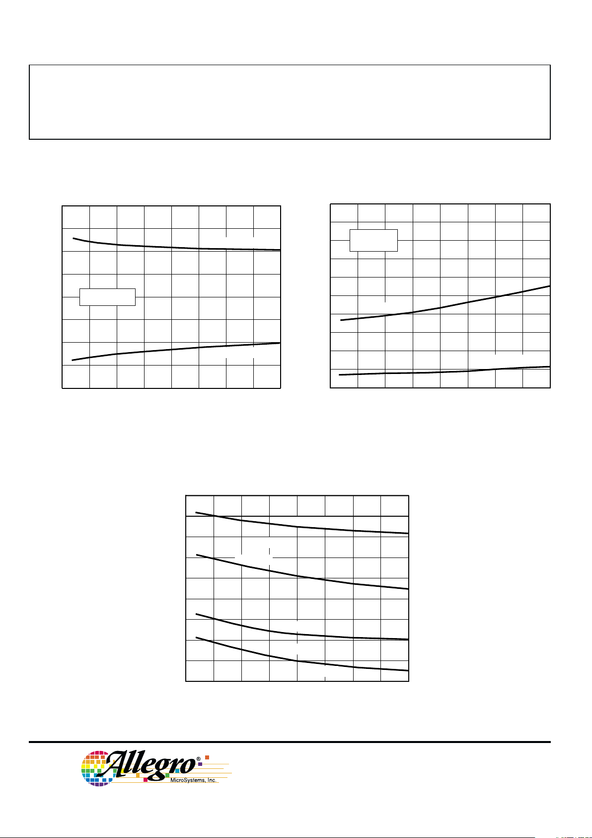
TYPICAL OPERATING CHARACTERISTICS
Output Saturation Voltage
Supply Current
0 25 50 75 100
AMBIENT TEMPERATURE IN °C
-50
Dwg. GH-052-2
125-25
SWITCH POINTS IN GAUSS
200
100
0
-100
-200
RELEASE POINT
OPERATE POINT
150
V = 5 V–24
V
CC
Switch Points
4.0
SUPPLY CURRENT IN mA
8.0
7.0
6.0
5.0
0 255075100
AMBIENT TEMPERATURE IN °C
-50
Dwg. GH-028-3
125-25 150
V = 5 V
CC
V = 5 V
CC
B ≥ B
OP
B ≤ B
RP
V = 24 V
CC
V = 24 V
CC
0 25 50 75
100
500
0
AMBIENT TEMPERATURE IN °C
400
200
-50
Dwg. GH-040-3
SATURATION VOLTAGE IN mV
150
-25
125
I = 30 m
A
OUT
300
100
CC
V = 12
V
I = 5 m
A
OUT
B ≥ B
OP
Page 5

3197
PROTECTED, HIGH-TEMP.,
OPEN-COLLECTOR
HALL-EFFECT LATCH
www.allegromicro.com
26 V
MAX
0+B
0
OUTPUT VOLTAGE IN VOLTS
FLUX DENSITY
Dwg. GH-034-2A
-B
RP
B
V
OUT(SAT)
BB
V
OP
B
OPERATION
In operation, the output transistor is OFF
until the strength of the magnetic field
perpendicular to the surface of the chip
exceeds the threshold or operate point (B
OP
).
When the field strength exceeds B
OP
, the
output transistor switches ON
(a logic low) and is capable of sinking
35 mA of current.
The output transistor switches OFF (a
logic high) when magnetic field reversal
results in a magnetic flux density below the
OFF threshold (B
RP
). This is illustrated in
the transfer characteristics graph. Note that
the device latches; that is, a south pole of
sufficient strength will turn the device ON.
Removal of the south pole will leave the
device ON. The presence of a north pole of
sufficient strength is required to turn the
device OFF.
The switch points increase in sensitivity
with increasing temperature to compensate
for the typical ferrite magnet temperature
characteristic. The simplest form of magnet
that will operate these devices is a ring
magnet. Other methods of operation are
possible.
TEST CIRCUIT AND TYPICAL APPLICATION
TO µP
3
X
Dwg. EH-006A
V
CC(UV)
TO 26 V
WITH TRANSIENTS
L
R
L
C
REGULATED
< 26 V
V
BB
V
CC
BYPASS
C
2
1
Page 6

3197
PROTECTED, HIGH-TEMP.,
OPEN-COLLECTOR
HALL-EFFECT LATCH
115 Northeast Cutoff, Box 15036
Worcester, Massachusetts 01615-0036 (508) 853-5000
Power Supply Transients (Noise);
Overvoltage and Undervoltage Lockout.
Even in protected devices, positive and
negative power supply transients that would
not normally cause physical damage can cause
logic errors in control systems. The A3197LT
and A3197LU include noise suppression
features to prevent this.
In a typical application, where the output
is externally pulled up to a regulated voltage
<28 V, the effects of power supply transients
on the device output are suppressed by turning
the output driver OFF during the first
undervoltage, V
CC(UV)
, (or negative) condition,
or first overvoltage (positive) condition,
V
CC(OV)
, and maintaining a power up reset
mode until normal power is restored. Note
that after the initial transient, the output does
not change logic state during subsequent
power supply noise pulses.
An external 0.1 µF to 0.5 µF capacitor,
with good high-frequency characteristics,
should be connected between terminals 1 and 2
to bypass high-voltage noise and reduce EMI
susceptibility.
B
OP
B
RP
V
CC
V
OUT
FIRST BOP AFTER
TRANSIENT(S)
Dwg. WH-007-2A
0
0
V
OUT
CLASSICAL OUTPUT RESPONSE
A3197– OUTPUT RESPONSE
Power Up Reset. These devices are designed to power up with the output OFF
without regard to any magnetic field applied.
The output will remain OFF until the flux is
reduced to below BRP (S-N transition) and then
BOP is exceeded, depending on the turn-on
state of the internal latches.
B
OP
B
RP
V
CC
V
OUT
FIRST BOP AFTER
POWER UP
Dwg. WH-006
0
0
V
OUT(SAT)
+B
-B
B
OP
B
RP
0
V
CC
V
OUT
FIRST BOP AFTER
TRANSIENT(S)
Dwg. WH-007-1A
0
V
OUT
CLASSICAL OUTPUT RESPONSE
A3197– OUTPUT RESPONSE
Page 7

3197
PROTECTED, HIGH-TEMP.,
OPEN-COLLECTOR
HALL-EFFECT LATCH
www.allegromicro.com
ISO
Pulse No. Test Test Conditions (over operating temperature range)
1 Inductive Turn Off (Negative) V
S
= -100 V, RS = 10 Ω, tr = 1 µs, td = 2 ms
2 Inductive Turn Off (Positive) V
S
= 100 V, RS = 10 Ω, tr = 1 µs, td = 50 µs
3a Capacitive/Inductive Coupling (Neg) V
S
= -150 V, RS = 50 Ω, tr = 50 ns, td = 100 ns
3b Capacitive/Inductive Coupling (Pos) V
S
= 100 V, RS = 50 Ω, tr = 50 ns, td = 100 ns
4 Reverse Battery V
S
= -14 V, td = 20 s
5 Load Dump (ISO) V
S
= 86.5 V, RS = 0.5 Ω, tr = 5 ms, td = 400 ms
(DIN) V
S
= 120 V, RS = 0.5 Ω, tr = 100 ns, td = 400 ms
6 Ignition Coil Disconnect V
S
= -300 V, RS = 30 Ω, tr = 60 µs, td = 300 µs
EXTERNAL PROTECTION REQ’D
7 Field Decay (Negative) V
S
= -80 V, RS = 10 Ω, tr = 5 ms, td = 100 ms
INTERNAL PROTECTIVE FEATURES
Power supply voltage transients, or device output short circuits,
may be caused by faulty connectors, crimped wiring harnesses, or
service errors. To prevent catastrophic failure, internal protection
against overvoltage, reverse voltage, output overloads, and thermal
stress have been incorporated to meet the automotive 12 volt system
protection requirements of ISO DP7637/1 and DIN 40839-1. A seriesblocking diode or current-limiting resistor is required in order to
survive pulse number six.
0
12 V
V
S
t
r
t
d
0.9 V
0.1 V
S
S
Dwg. WH-008
Page 8

3197
PROTECTED, HIGH-TEMP.,
OPEN-COLLECTOR
HALL-EFFECT LATCH
115 Northeast Cutoff, Box 15036
Worcester, Massachusetts 01615-0036 (508) 853-5000
Test Method and No. of Samples
Qualification Test Test Conditions Lots Test Length Per Lot Comments
Biased Humidity JESD22-A101 3 1200 hrs 116 Device biased for
T
A
= 85°C, RH = 85% minimum power
High-Temperature JESD22-A108 3 1200 hrs 116
Operating Life T
A
= 150°C, TJ = 165°C
Surge Operating Life JESD22-A108 1 504 hrs 116
T
A
= 175°C, TJ = 190°C
Pressure Cooker, JESD22-A102, Method C 3 96 hrs 77
Unbiased
Storage Life MIL-STD-883, Method 1008 1 1200 hrs 77
T
A
= 170°C
Temperature Cycle MIL-STD-883, Method 1010 3 1000 cycles 153
ESD MIL-STD-883, Method 3015 1 Pre/Post 3 per Test to failure
Human Body Model Reading test HBM > 16 kV
ESD 1 Pre/Post 3 per Test to failure
Machine Model Reading test MM > 800 V
Output Overloads. Current through the output transistor is sensed with a low-value on-chip aluminum resistor.
The voltage drop across this resistor is fed back to control
the base drive of the output stage. This feedback prevents
the output transistor from exceeding its maximum current
density rating by limiting the output current to between
35 mA and 70 mA. Under short-circuit conditions, the
device will dissipate an increased amount of power (P
D
=
V
OUT
x I
LIMIT
) and the output transistor will be thermally
stressed.
Thermal Stress. When thermal stresses (either internal
or external) cause the junction temperature to exceed
+165°C, thermal shutdown of the output transistor is
activated. The thermal shutdown circuitry only provides
protection against thermal stresses caused by increased
power dissipation of the output transistor.
Overvoltage. The device protects itself against highvoltage transients by shutting OFF all supply-referenced
active components, reducing the supply current, and
minimizing device power dissipation. Overvoltage
shutdown can occur anywhere between 28 V and 55 V and
device operation above 28 V cannot be recommended.
Under a sustained overvoltage, the device may be required
to dissipate an increased amount of power (PD = VCC x
ICC) and the device may be thermally stressed (see above).
Output Voltage. The output is clamped with an on-chip
Zener diode to limit the maximum output voltage that can
occur during overvoltage faults or when switching an
inductive load.
When any fault condition is removed, the device returns to
normal operating mode.
CRITERIA FOR DEVICE QUALIFICATION
All Allegro sensors are subjected to stringent qualification requirements prior to being released to production. To
become qualified, except for the destructive ESD tests, no failures are permitted.
Page 9

3197
PROTECTED, HIGH-TEMP.,
OPEN-COLLECTOR
HALL-EFFECT LATCH
www.allegromicro.com
APPLICATIONS INFORMATION
The A3197LLT and A3197LU latches have been optimized for
use in automotive ring magnet sensing applications. Such applications
include transmission speed sensors, motor position encoders, and wheel
bearing speed sensors. Special care has been taken to optimize the
operation of these devices in automotive subsystems that require ISO
DP9637 protection but NOT operation. Undervoltage lockout is included to prevent propagation of false logic pulses during low battery,
cold-start conditions. Noise suppression is included to prevent false
switching of the device when subjected to ISO transients. Short-circuit
protection is included to prevent damage caused by pinched wiring
harnesses.
A typical application consists of a ferrite ring magnet located on a
rotating shaft. Typically, this shaft is attached to the transmission, the
sensor is mounted on a board, with care being taken to keep a tight
tolerance on the air gap between the package face and the magnet. The
device will provide a change in digital state at the transition of every
magnetic pole and, thus, give an indication of the transmission speed.
The high magnetic hysteresis allows the device to be immune to vibration of the magnet shaft and relatively good duty cycles can be obtained.
Hall effect applications information is available in the “Hall-Effect
IC Applications Guide”, which can be found in the Allegro
MicroSystems Electronic Data Book, AMS-702, or Application Note
2770, or at
www.allegromicro.com.
SENSOR LOCATIONS
(±0.005" [0.13 mm] die placement)
SUFFIX “LT”
SUFFIX “U”
A
1 32
Dwg. MH-008-5A
0.030"
0.76 mm
NOM
ACTIVE AREA DEPTH
0.051"
1.30 mm
0.092"
2.35 mm
A
1 3
Dwg. MH-002-12A
0.015"
0.38 mm
NOM
0.073"
1.85 mm
BRANDED
SURFACE
ACTIVE AREA DEPTH
2
0.094"
2.40 mm
Page 10

3197
PROTECTED, HIGH-TEMP.,
OPEN-COLLECTOR
HALL-EFFECT LATCH
115 Northeast Cutoff, Box 15036
Worcester, Massachusetts 01615-0036 (508) 853-5000
A3197ELT and A3197LLT
Dimensions in Inches
(for reference only)
Dimensions in Millimeters
(controlling dimensions)
NOTE — Exact body and lead configuration at vendor’s option within limits shown.
Dwg. MA-009-3A mm
1
23
4.60
4.40
1.83
1.62
4.25
3.94
1.50
BSC
0.48
0.36
1.20
0.89
2.60
2.29
1.60
1.40
0.44
0.35
2.29
2.13
0.56
0.44
3.00
BSC
Dwg. MA-009-3A in
1
23
0.072
0.064
0.167
0.155
0.059
BSC
0.0189
0.0142
0.047
0.035
0.102
0.090
0.063
0.055
0.0173
0.0138
0.090
0.084
0.0221
0.0173
0.118
BSC
0.181
0.173
Page 11

3197
PROTECTED, HIGH-TEMP.,
OPEN-COLLECTOR
HALL-EFFECT LATCH
www.allegromicro.com
A3197EU and A3197LU
Dimensions in Inches Dimensions in Millimeters
(controlling dimensions) (for reference only)
NOTES:1. Tolerances on package height and width represent allowable mold offsets.
Dimensions given are measured at the widest point (parting line).
2. Exact body and lead configuration at vendor’s option within limits shown.
3. Height does not include mold gate flash.
4. Recommended minimum PWB hole diameter to clear transition area is 0.035" (0.89 mm).
5. Where no tolerance is specified, dimension is nominal.
Dwg. MH-003E in
0.063
0.059
0.018
0.0173
0.0138
0.0189
0.0142
0.050
1 2 3
0.100
45°
SEE NOTE
0.183
0.178
0.181
0.176
0.600
0.560
0.086
MAX
Dwg. MH-003E mm
1.60
1.50
0.46
0.44
0.35
0.48
0.36
1.27
1 2 3
2.54
45°
SEE NOTE
4.65
4.52
4.60
4.47
15.24
14.23
2.18
MAX
Page 12

3197
PROTECTED, HIGH-TEMP.,
OPEN-COLLECTOR
HALL-EFFECT LATCH
115 Northeast Cutoff, Box 15036
Worcester, Massachusetts 01615-0036 (508) 853-5000
The products described herein are manufactured under one or more
of the following U.S. patents: 5,045,920; 5,264,783; 5,442,283;
5,389,889; 5,581,179; 5,517,112; 5,619,137; 5,621,319; 5,650,719;
5,686,894; 5,694,038; 5,729,130; 5,917,320; and other patents
pending.
Allegro MicroSystems, Inc. reserves the right to make, from time to
time, such departures from the detail specifications as may be required
to permit improvements in the performance, reliability, or
manufacturability of its products. Before placing an order, the user is
cautioned to verify that the information being relied upon is current.
Allegro products are not authorized for use as critical components
in life-support appliances, devices, or systems without express written
approval.
The information included herein is believed to be accurate and
reliable. However, Allegro MicroSystems, Inc. assumes no responsibility for its use; nor for any infringements of patents or other rights of
third parties that may result from its use.
 Loading...