

Datasheet A3054SU-30, A3054SU-29, A3054SU-28, A3054SU-27, A3054SU-26 Datasheet (Allegro)
...Page 1
3054
MULTIPLEXED
TWO-WIRE
HALL-EFFECT SENSOR ICs
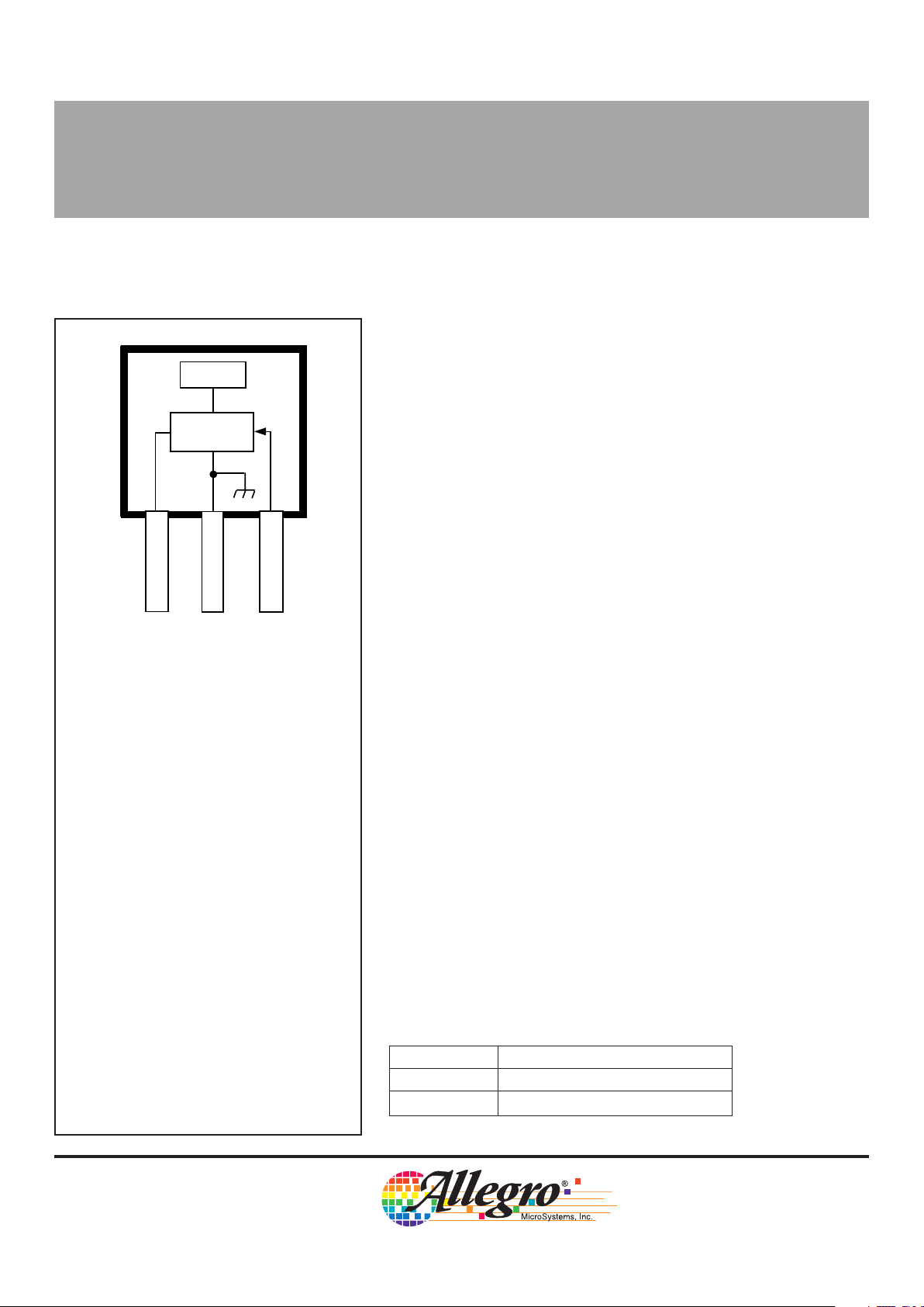
The A3054KU and A3054SU Hall-effect sensors are digital magnetic sensing ICs capable of communicating over a two-wire power/
signal bus. Using a sequential addressing scheme, the device responds to a signal on the bus and returns the diagnostic status of the
IC, as well as the status of each monitored external magnetic field.
As many as 30 sensors can function on the same two-wire bus. This
IC is ideal for multiple sensor applications where minimizing the wiring
harness size is desirable or essential.
Each device consists of high-resolution bipolar Hall-effect switching circuitry, the output of which drives high-density CMOS logic
stages. The logic stages decode the address pulse and enable a
response at the appropriate address. The combination of magneticfield or switch-status sensing, low-noise amplification of the Halltransducer output, and high-density decoding and control logic is made
possible by the development of a new sensor DABiC™ (digital analog
bipolar CMOS) fabrication technology. The A3054SU is an improved
replacement for the original UGN3055U.
These unique magnetic sensing ICs are available in two temperature ranges; the A3054SU operates within specifications between
-20°C and +85°C, while the A3054KU is rated for operation between
-40°C and +125°C. Alternative magnetic and temperature specifications are available on special order. Both versions are supplied in
0.060" (1.54 mm) thick, three-pin plastic SIPs. Each device is clearly
marked with a two-digit device address (XX).
3054
MULTIPLEXED TWO-WIRE
HALL-EFFECT SENSOR ICs
FEATURES
■ Complete Multiplexed Hall-Effect ICs with
Simple Sequential Addressing Protocol
■ Allows Power and Communication Over a
Two-Wire Bus (Supply/Signal and Ground)
■ Up to 30 Hall-Effect Sensors Can Share a Bus
■ Sensor Diagnostic Capabilities
■ Magnetic-Field or Switch-Status Sensing
■ Low Power of DABiC Technology Favors
Battery-Powered and Mobile Applications
■ Ideal for Automotive, Consumer, and Industrial Applications
Always order by complete part number:
Part Number Operating Temperature Range
A3054KU-XX -40°C to +125°C
A3054SU-XX -20°C to +85°C
where XX = address (01, 02, … 29, 30).
Pinning is shown viewed from branded side.
ABSOLUTE MAXIMUM RATINGS
at T
A
= +25°C
Supply Voltage, V
BUS
. . . . . . . . . . . . . . 18 V
Magnetic Flux Density, B . . . . . . . Unlimited
Operating Temperature Range, T
A
A3054KU . . . . . . . . . . . -40°C to +125°C
A3054SU . . . . . . . . . . . . -20°C to +85°C
Storage Temperature Range,
TS. . . . . . . . . . . . . . . . . -55°C to +150°C
Package Power Dissipation,
PD. . . . . . . . . . . . . . . . . . . . . . . 635 mW
Data Sheet
27680.1
Dwg. PH-005
1
BUS
GROUND
32
SWITCH IN
X
LOGIC
Page 2

3054
MULTIPLEXED
TWO-WIRE
HALL-EFFECT SENSOR ICs
115 Northeast Cutoff, Box 15036
Worcester, Massachusetts 01615-0036 (508) 853-5000
Limits
Characteristic Symbol Test Conditions Min Typ Max Units
Power Supply Voltage V
BUS
——15 V
Signal Current I
S
DUT Addressed, B > 300 G 12 15 20 mA
Quiescent Current I
QL
V
BUS
= 6 V — 1.5 2.5 mA
I
QH
V
BUS
= 9 V — 1.4 2.5 mA
∆I
Q
I
QL
– I
QH
— 100 300 µA
Address Range Addr Factory Specified 1 — 30 —
Clock Thresholds V
CLH
LOW to HIGH — — 8.5 V
V
CHL
HIGH to LOW 6.5 — — V
V
CHYS
Hysteresis — 0.8 — V
Max. Clock Frequency* f
CLK
50% Duty Cycle 2.5 — — kHz
Address LOW Voltage V
L
V
RST
6.0 V
CHL
V
Address HIGH Voltage V
H
V
CLH
9.0 V
BUS
V
Reset Voltage V
RST
2.5 3.5 5.5 V
Propagation Delay* t
plh
LOW to HIGH 10 20 30 µs
t
phl
HIGH to LOW — 5.0 10 µs
Pin 3-2 Resistance R
SWH
DUT Addressed, B < 5 G — 50 — kΩ
R
SWL
DUT Addressed, B > 300 G — 200 — Ω
Pin 3-2 Output Voltage V
SWH
DUT Addressed, B < 5 G — 3.9 — V
V
SWL
DUT Addressed, B> 300 G — 30 — mV
MAGNETIC CHARACTERISTICS over operating temperature range.
Limits
Characteristic Symbol Test Conditions Min. Typ. Max. Units
Magnetic Threshold† B
OP
Turn-On 50 150 300 G
B
RP
Turn-Off 5.0 100 295 G
Hysteresis B
HYS
B
OP
– B
RP
5.0 50 — G
ELECTRICAL CHARACTERISTICS over operating temperature range.
Typical Data is at TA = +25°C and is for design information only.
*This parameter, although warranteed, is not production tested.
†Alternative magnetic switch point specifications are available on special order. Please contact the factory.
W
Copyright © 1995 Allegro MicroSystems, Inc.
Page 3
3054
MULTIPLEXED
TWO-WIRE
HALL-EFFECT SENSOR ICs
FUNCTIONAL BLOCK DIAGRAMSENSOR LOCATION
(±0.005” [0.13 mm] die placement)
CLOCK
Dwg. FH-009
BUS
SWITCH IN
(OPTIONAL)
GROUND
CMOS LOGIC
REG
COMP COMP
RESET
1
3
2
1 32
Dwg. MH-002-10A
0.015"
0.38 mm
NOM
BRANDED
SURFACE
ACTIVE AREA DEPTH
0.073"
1.85 mm
A
0.090"
2.29 mm
DEFINITION OF TERMS
Sensor Address
Each bus sensor has a factory-specified predefined
address. At present, allowable sensor addresses are
integers from 01 to 30.
LOW-to-HlGH Clock Threshold (V
CLH
)
Minimum voltage required during the positive-going
transition to increment the bus address and trigger a
diagnostic response from the bus sensors. This is also
the maximum threshold of the on-chip comparator that
monitors the supply voltage, V
BUS
.
HlGH-to-LOW Threshold (VHL)
Maximum voltage required during the negative-going
transition to trigger a
signal
current response from the bus
sensors. This is also the maximum threshold of the
on-chip comparator that monitors the supply voltage,
V
BUS
.
Bus HIGH Voltage (VH)
Bus HIGH voltage during addressing. Voltage should
be greater than V
CLH
.
Address LOW Voltage (VL)
Bus LOW voltage during addressing. Voltage should
be greater than V
RST
and less than V
CHL
.
Bus Reset Voltage (V
RST
)
Voltage level while resetting sensors.
Sensor Quiescent Current Drain (IQ)
The current drain of bus sensors when active but not
addressed. IQH is the quiescent current drain when the
sensor is not addressed and is at VH IQL is the quiescent
current drain when the sensor is not addressed and is at
VL. Note that IQL is greater than IQH.
Diagnostic Phase
Period on the bus when the address voltage is at VH.
During this period, a correctly addressed sensor responds
by increasing its current drain on the bus. This response
from the sensor is called the diagnostic response and
the bus current
increase
is called the diagnostic current.
Signal Phase
Period on the bus when the address voltage is at VL.
During this period, a correctly addressed sensor that
detects a magnetic field greater than the magnetic operate point, BOP, responds by maintaining a current drain of
IS on the bus. This response from the sensor is called the
signal response and the bus current is called the signal
current.
Sensor Address Response Current (IS)
Sensor current during the
diagnostic
and the
signal
responses of the bus sensor. This is accomplished by
enabling an internal constant-current source.
Page 4
3054
MULTIPLEXED
TWO-WIRE
HALL-EFFECT SENSOR ICs
115 Northeast Cutoff, Box 15036
Worcester, Massachusetts 01615-0036 (508) 853-5000
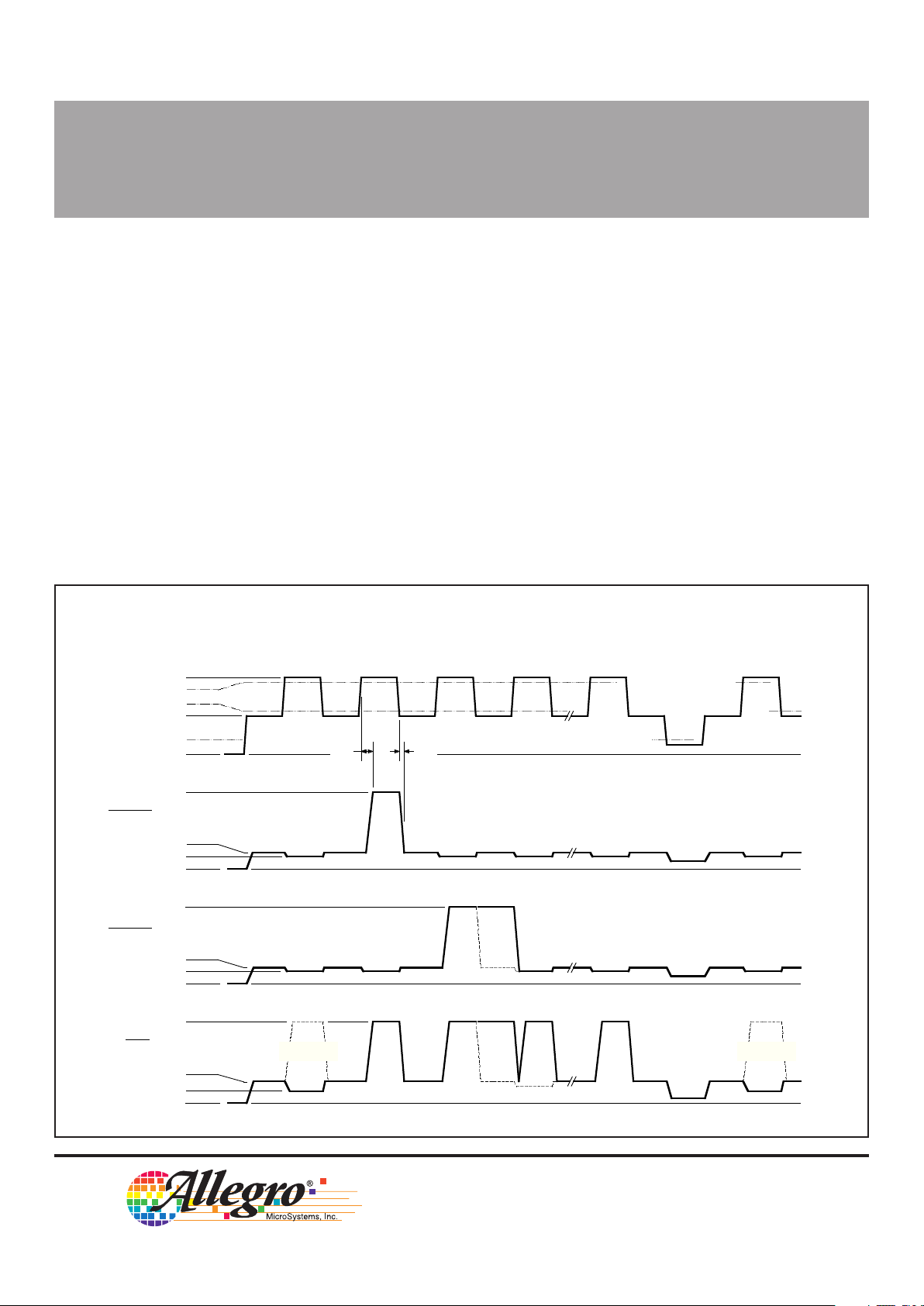
A device may be addressed by changing the supply
voltage as shown in Figure 1. A preferred addressing
protocol is as follows: the bus supply voltage is brought
low (<2.5 V) so that all devices on the bus are reset. The
voltage is then raised to the address LOW voltage (VL) and
the bus quiescent current is measured. The bus is then
toggled between VL and VH (address HIGH voltage), with
each positive transition representing an increment in the
bus address. After each voltage transition, the bus current
may be monitored to check for diagnostic and signal
responses from sensor ICs.
Sensor Addressing
When a sensor detects a bus address equal to its
factory-programmed address, it responds with an increase
in its supply current drain ( IS) during the next HIGH portion
ADDRESSING PROTOCOL
Magnetic Operate Point (BOP)
Minimum magnetic field required to switch ON the
Hall amplifier and switching circuitry of the addressed
sensor. This circuitry is only active when the sensor is
addressed.
Magnetic Release Point (BRP)
Magnetic field required to switch OFF the Hall
amplifier and switching circuitry after the output has been
switched ON. When a device is deactivated by changing
the bus address, all magnetic memory is lost.
Magnetic Hysteresis (B
HYS
)
Difference between the BOP and BRP magnetic field
thresholds.
FIGURE 1
BUS TIMING
SENSOR 03 — DIAGNOSTIC
AND SIGNAL CURRENTS
DIAGNOSTIC
ADDRESS 01
DIAGNOSTIC
ADDRESS 02
DIAGNOSTIC
ADDRESS 04
DIAGNOSTIC
ADDRESS
n
RESET
DIAGNOSTIC
ADDRESS 01
SENSOR 02 —
DIAGNOSTIC CURRENT
DIAGNOSTIC
ADDRESS 03
SENSOR 01
NOT PRESENT
V
H
V
L
V
RST
0
I
S
I
QL
I
QH
0
I
S
0
I
S
n • I
QL
n • I
QH
0
t
phl
t
plh
V
CLH
V
CHL
Dwg. WH-005
BUS
VOLTAGE
SENSOR 02
CURRENT
WITH NO
MAGNETIC
FIELD
SENSOR 03
CURRENT
WITH
MAGNETIC
FIELD
TOTAL
BUS CURRENT
WITH
MAGNETIC
FIELD AT
SENSOR 03
RESET
I
QL
I
QH
SENSOR 01
NOT PRESENT
Page 5

3054
MULTIPLEXED
TWO-WIRE
HALL-EFFECT SENSOR ICs
ofthe address cycle. This response may be
used as an indication that the sensor is "alive
and well" on the bus and is called the
diag-
nostic
response. If the sensor detects an
ambient magnetic field, it continues with I
S
during the low portion of the address cycle.
This response from the sensor is called the
signal
response. When the next positive
(address) transition is detected, the sensor
becomes disabled, and its contribution to the
bus signal current returns to IQ.
Bus Current
Figure 1 shows the addressing protocol.
The top trace represents the bus voltage
transitions as controlled by the bus driver
(see Applications Notes for an optimal bus
driver schematic). The second trace represents the bus current contribution of Sensor
02. The
diagnostic
response from the sensor
indicates that it detected its address on the
bus. However, no
signal
current is shown,
which indicates that sufficient magnetic field
is not detected at the chip surface and that
pin 3 is open circuited. The third trace
represents the current drain of Sensor 03
when a magnetic field is detected. Note both
the
diagnostic
and
signal
currents from the
sensor. The last trace represents the overall
bus current drain. When no sensors are
addressed, the net bus current is the sum of
quiescent currents of all sensors on the bus
(for 'n' sensors, the bus current drain is
n • IQ).
Bus Issues
After a reset, while at the address LOW
voltage (VL), and before the first address
pulse, bus current calibration may be performed. This feature allows for fail-safe
detection of signal current and eliminates
detection problems caused by low signal
current (IS), the operation of sensors at
various ambient temperatures, lot-to-lot
variation of quiescent current, and the
addition or replacement of sensors to the bus
while in the field. At present, a maximum of
30 active sensors can coexist on the same
bus, each with a different address. Address
TYPICAL DEVICE QUIESCENT CURRENT
FIGURE 2
SENSOR CONNECTIONS
Dwg. EH-004
1 32
1 32
NC
SWITCH
POSITIVE BUS SUPPLY
BUS RETURN
X
X
6
91215
SUPPLY VOLTAGE, V IN VOLTS
0
Dwg. GH-045
3
QUIESCENT CURRENT, I IN mA
0
0.5
1.0
1.5
2.0
T = +25°C
A
BUS
Q
Page 6

3054
MULTIPLEXED
TWO-WIRE
HALL-EFFECT SENSOR ICs
115 Northeast Cutoff, Box 15036
Worcester, Massachusetts 01615-0036 (508) 853-5000
ADDRESS
RESET
ANALOG OUT
(POSITIVE) BUS SUPPLY
BUS RETURN
MICROPROCESSOR
INTERFACE
01 02 28 29 30
Dwg. EH-005
31 is designed to be inactive to allow for
further address expansion of the bus (to 62
maximum addresses). In order to repeat the
address cycle, the bus must be reset, as
shown in Figure 1, by bringing the supply
voltage to below V
RST
. Sensors have been
designed not to ‘wrap-around’.
Magnetic Sensing
The sensor IC has been designed to
respond to an external magnetic field whose
magnetic strength is greater than BOP. It
accomplishes this by amplifying the output of
an on-chip Hall transducer and applying it to
a threshold detector. In order that bus
current is kept to a minimum, the transducer
and amplification circuitry is kept powered
down until the sensor is addressed. Hence,
the magnetic status is evaluated only when
the sensor is addressed.
External Switch Sensing
Pin 3 of the IC may be used to detect the
status of an external switch when magnetic
field sensing is not desired (and in the
absence of a magnetic field). The allowable
states for the switch are ‘open’ or ‘closed’
(shorted to sensor ground).
APPLICATIONS NOTES
Magnetic Actuation
The left side of Figure 2 shows the wiring of an A3054KU or
A3054SU when used as a magnetic threshold detector. Pin 1 of the
sensor is wired to the positive terminal of the bus, pin 2 is connected to
the bus negative terminal, and
pin 3 has no connection.
Mechanical Actuation
The right side of Figure 2 shows the wiring of an A3054KU or
A3054SU when used to detect the status of a mechanical switch.
In this case, pin 3 is connected to the switch. The other side of the
switch is connected to the bus return (negative bus supply or ground).
When the mechanical switch is closed, and the correct bus address is
detected by the IC, the sensor responds with a signal current. If the
switch is open, only the diagnostic current is returned.
Bus Configuration
A maximum of 30 individually addresable sensors may be connected across the same two-wire bus as shown in Figure 3. It is
recommended that the sensors use a dedicated digital ground wire to
minimize the effects of changing ground potential (as in the case of
chassis ground in the automotive industry).
The bus was not designed to require two-wire twisted pair wiring to
the sensors. However, in areas of extreme electromagnetic interference, it may be advisable to install a small bypass capacitor (0.01 µF
for example) between the supply and ground terminals of each sensor
instead of using the more expensive wiring.
FIGURE 3
BUS INTERCONNECTION
Page 7

3054
MULTIPLEXED
TWO-WIRE
HALL-EFFECT SENSOR ICs
Bus Driver
It is recommended that the bus be controlled
by microprocessor-based hardware for the
following reasons:
• Sensor address information may be stored
in ROM in the form of a look-up table.
• Bus faults can be pinpointed by the
microprocessor by comparing the diagnostic response to the expected response in
the ROM look-up table.
• The microprocessor, along with an A/D
converter, can also be used to self calibrate the quiescent currents in the bus and
hence be able to easily detect a signal
response.
• The microprocessor can also be used to filter out random line noise
by digitally filtering the bus responses.
• The microprocessor can easily keep track of the signal responses
and initiate the appropriate action (e.g., light a lamp or sound an
alarm, and also pinpoint the location of the signal).
Optimally, the microprocessor is used to control bus-driving
circuitry that will accept TTL-level inputs to drive the bus and will return
an analog voltage representation of the bus current.
Interface Schematic
The bus driver is easily designed using a few operational amplifiers, resistors, and transistors. Figure 4 shows a schematic of a
recommended bus driver circuit that is capable of providing 6 V to 9 V
transitions, resetting the bus, and providing an analog measurement of
the bus current for the A/D input of the microprocessor.
FIGURE 4
BUS INTERFACE SCHEMATIC
50 kΩ
Dwg. EH-003A
1 32
1 32
+15 V
1 kΩ
10 kΩ
9 V
20 kΩ
5 kΩ
5 kΩ
ADDRESS
RESET
1 kΩ
50 Ω
50 kΩ
100 kΩ
100 kΩ
NC
SWITCH
BUS SUPPLY
BUS RETURN
X
X
ANALOG OUT
0.001
µF
R
5
R
8
R
9
R
10
R
7
R
6
Q
1
Q
2
Z
1
R
4
OP
1
OP
2
Q
3
Page 8

3054
MULTIPLEXED
TWO-WIRE
HALL-EFFECT SENSOR ICs
115 Northeast Cutoff, Box 15036
Worcester, Massachusetts 01615-0036 (508) 853-5000
In Figure 4, the ADDRESS input provides a TTL-compatible input
to control the bus supply. A HIGH (5 V) input switches Q1 ON and sets
the bus voltage to 6 V through the resistor divider R4, R5, and Zener
Z1. A LOW input switches Q1 OFF and sets the bus voltage to 9 V
(Z1). This voltage is fed into the positive input of the operational
amplifier OP1 and is buffered and made available at BUS SUPPLY (or
sensor supply). Bus reset control is also available in the form of a TTLcompatible input. When the RESET input is HIGH, Q2 is switched ON
and the positive input of the operational amplifier is set to the saturation voltage of the transistor (approximately 0 V). This resets the bus.
A linear reading of the bus current is made possible by amplifying
the voltage generated across R6 (which is I
BUS
• R6). The amplifier,
OP2, is a standard differential amplifier of gain R9/R7 (provided that R
7
= R8, R9 = R10). The gain of the total transim-pedance amplifier is
given by:
V
OUT
= I
BUS
• R6 • R9/R
7
This voltage is available at the ANALOG OUT terminal.
Bus Control Software
The processing of the bus current (available at ANALOG OUT) is
best done by feeding it into the A/D input of a microprocessor. If the
flexibility provided by a microprocessor is not desired, this signal could
be fed into threshold detection circuitry; e.g., comparator, and the
output used to drive a display.
Related References
1. G. AVERY, “Two-Terminal Hall Sensor,”
ASSIGNEE: Sprague
Electric Company, North Adams, MA, United States. Patent number
4,374,333; Feb. 1983.
2. T. WROBLEWSKI and F. MEISTERFIELD, “Switch Status
Monitoring System, Single-Wire Bus, Smart Sensor Arrangement
There Of,”
ASSIGNEE: Chrysler Motor Corporation, Highland Park, Ml,
United States. Patent number 4,677,308; June 1987.
Page 9

3054
MULTIPLEXED
TWO-WIRE
HALL-EFFECT SENSOR ICs
Dimensions in Inches
(controlling dimensions)
Dimensions in Millimeters
(for reference only)
NOTES: 1. Tolerances on package height and width represent allowable mold offsets.
Dimensions given are measured at the widest point (parting line).
2. Exact body and lead configuration at vendor’s option within limits shown.
3. Height does not include mold gate flash.
4. Recommended minimum PWB hole diameter to clear transition area is
0.035” (0.89 mm).
5. Where no tolerance is specified, dimension is nominal.
6. Minimum lead length was 0.500” (12.70 mm). If existing product to the
original specifications is not acceptable, contact sales office before
ordering.
Dwg. MH-003D mm
1.60
1.50
0.46
0.38
0.41
1.27
1 2 3
2.54
45°
SEE NOTE
4.65
4.52
4.60
4.47
15.24
14.23
2.18
MAX
Dwg. MH-003D in
0.063
0.059
0.018
0.015
0.016
0.050
1 2 3
0.100
45°
SEE NOTE
0.183
0.178
0.181
0.176
0.600
0.560
0.086
MAX
Page 10

3054
MULTIPLEXED
TWO-WIRE
HALL-EFFECT SENSOR ICs
115 Northeast Cutoff, Box 15036
Worcester, Massachusetts 01615-0036 (508) 853-5000
This page intentionally left blank
Page 11

3054
MULTIPLEXED
TWO-WIRE
HALL-EFFECT SENSOR ICs
Allegro MicroSystems, Inc. reserves the right to make, from time to time, such departures from
the detail specifications as may be required to permit improvements in the design of its products.
The information included herein is believed to be accurate and reliable. However, Allegro
MicroSystems, Inc. assumes no responsibility for its use; nor for any infringements of patents or
other rights of third parties which may result from its use.
Page 12

3054
MULTIPLEXED
TWO-WIRE
HALL-EFFECT SENSOR ICs
115 Northeast Cutoff, Box 15036
Worcester, Massachusetts 01615-0036 (508) 853-5000
HALL-EFFECT SENSORS SELECTION GUIDE
Partial Part Avail. Oper. ␣ Operate Limits Over Temp.␣
Number Temp. B
OP
max B
RP
min B
hys
min Function† Notes
3046 E/L +200 -200 15 Gear-Tooth Sensor
3054 K/S +300 +5 5.0 Unipolar Multiplex 1
3056 E/L +225 -225 15 Gear-Tooth Sensor
3058 E/L +300 -300 150 Gear-Tooth Sensor
3059 K/S +100 -100 20 AC Gear-Tooth Sensor
3060 K/S +35 -35 10 AC Gear-Tooth Sensor
3121 E/L +500 +80 60 Unipolar Switch
3122 E/L +430 +120 70 Unipolar Switch
3123 E/L +470 +160 70 Unipolar Switch
3132 K/L/S +95 -95 30 Bipolar Switch
3133 K/L/S +75 -75 30 Bipolar Switch
3134 E/L +50 -40 10 Bipolar Switch
3141 E/L +175 +10 20 Unipolar Switch
3142 E/L +245 +60 30 Unipolar Switch
3143 E/L +355 +150 30 Unipolar Switch
3144 E/L +450 +25 20 Unipolar Switch
3161 E +160 +30 5.0 2-Wire Unipolar Switch
3175 S +180 -180 80 Bipolar Latch
3177 S +150 -150 50 Bipolar Latch
3185 E/L +300 -300 280 Bipolar Latch
3187 E/L +175 -175 100 Bipolar Latch
3188 E/L +200 -200 160 Bipolar Latch
3189 E/L +250 -250 100 Bipolar Latch
3195 E/L +200 -200 110 Bipolar Latch 2, 3
3197 L +200 -200 110 Bipolar Latch 3
3235 S +200 +15 15 Unipolar Switch 4
-200 -15 15 Unipolar Switch
3275 S +250 -250 100 Bipolar Latch 5
3421 E/L +300 -300 240 Direction Detection
3422 E/L +85 -85 10 Direction Detection
3503 S Typ. 1.3 mV/G – Linear Sensor
3515 E/L Typ. 5.0 mV/G – Chopper-Stabilized Linear Sensor
3516 E/L Typ. 2.5 mV/G – Chopper-Stabilized Linear Sensor
3517 L/S Typ. 5.0 mV/G – Chopper-Stabilized Linear Sensor
3518 L/S Typ. 2.5 mV/G – Chopper-Stabilized Linear Sensor
3625 S +150 -150 200* 900 mA Bipolar Latch 3, 5, 6
3626 S +150 -150 200* 400 mA Bipolar Latch 3, 5, 6
5140 E +240 +25 20 300 mA Unipolar Switch 3, 6
Operating Temperature Ranges:
C = 0°C to +70°C, S = -20°C to +85°C, E = -40°C to +85°C, K = -40°C to +125°C, L = -40°C to +150°C
Notes 1. Multiplexed two-wire sensor; after proper address, power/signal bus current indicates magnetic field condition.
2. Active pull down.
3. Protected.
4. Output 1 switches on south pole, output 2 switches on north pole for 2-phase, bifilar-wound, unipolar-driven brushless dc motor control.
5. Complementary outputs for 2-phase bifilar-wound, unipolar-driven brushless dc motor control.
6. Power driver output.
* Typical.
† Latches will not switch on removal of magnetic field; bipolar switches may switch on removal of field but require field reversal for reliable operation
over operating temperature range.
 Loading...