

Page 1
2919
DUAL FULL-BRIDGE
MOTOR DRIVER
DUAL FULL-BRIDGE
PWM MOTOR DRIVER
A2919SB
1
2
3
4
5
6
7
8
9
24
23
22
21
20
19
18
17
16
15
14
13
12
11
10
9
θ
2
θ
1
V
CC
PWM 2
PWM 1
2
V
BB
1
GROUND
GROUND
GROUND
GROUND
02
I
12
I
PHASE
2
V
REF 2
2
RC
1
RC
V
REF 1
PHASE
1
11
I
2B
OUT
SENSE
2
2
E
2A
OUT
1A
OUT
1
E
SENSE
1
1B
OUT
01
I
LOAD
SUPPLY
LOGIC
SUPPLY
Dwg. PP-005
Data Sheet
29319.21
ABSOLUTE MAXIMUM RATINGS
at T
J ≤
150°C
Motor Supply Voltage, VBB................... 45 V
Output Current, I
OUT
(Peak, tw ≤ 20 µs)........................ ±1.0 A
(Continuous) ..........................
±750 mA
Logic Supply Voltage, V
CC
................... 7.0 V
Logic Input Voltage Range,
V
IN
............................... -0.3 V to +7.0 V
Output Emitter Voltage, V
E
.................. 1.5 V
Package Power Dissipation,
P
D
....................................... See Graph
Operating Temperature Range,
T
A
................................. -20°C to +85°C
Storage Temperature Range,
T
S
............................... -55°C to +150°C
Output current rating may be limited by duty cycle,
ambient temperature, and heat sinking. Under any
set of conditions, do not exceed the specified peak
current rating or a junction temperature of +150°C.
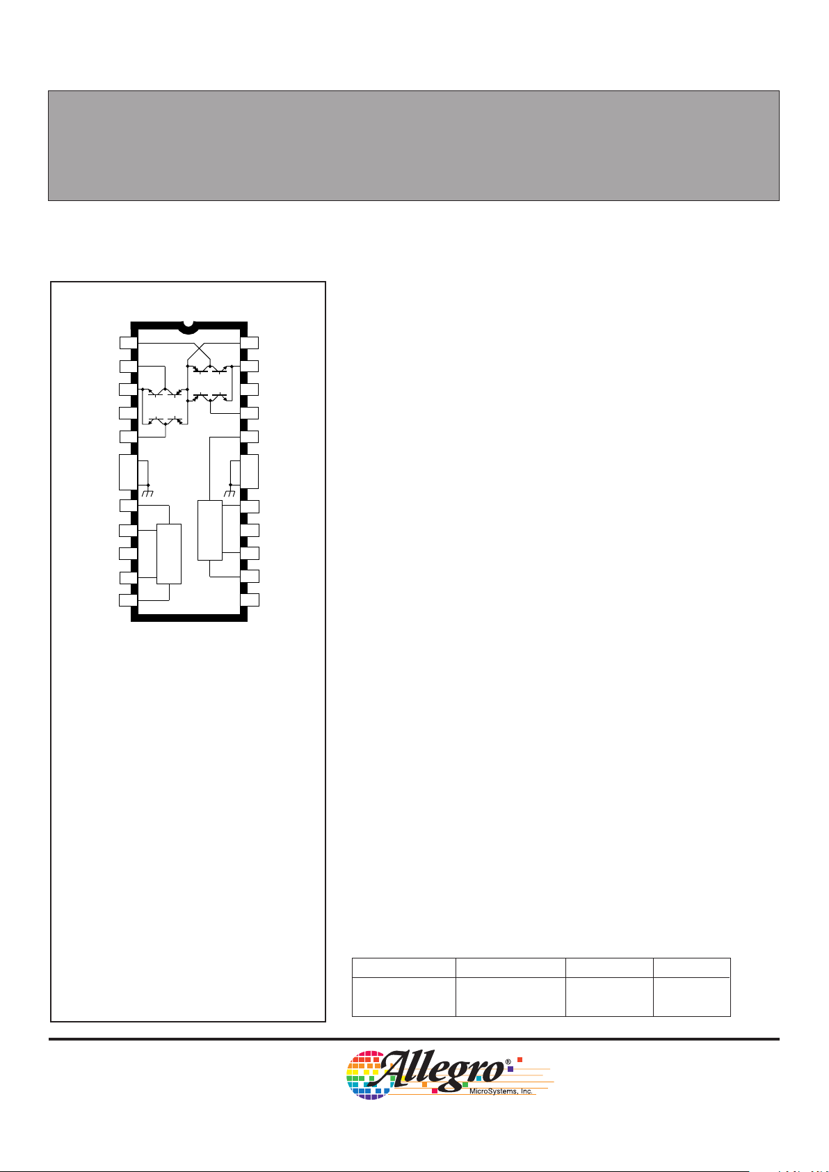
The A2919SB and A2919SLB motor drivers are designed to drive
both windings of a bipolar stepper motor or bidirectionally control two
dc motors. Both bridges are capable of sustaining 45 V and include
internal pulse-width modulation (PWM) control of the output current to
750 mA. The outputs have been optimized for a low output-saturation
voltage drop (less than 1.8 V total source plus sink at 500 mA).
For PWM current control, the maximum output current is determined by the user’s selection of a reference voltage and sensing
resistor. Two logic-level inputs select output current limits of 0%, 41%,
67%, or 100% of the maximum level. A PHASE input to each bridge
determines load current direction.
The bridges include both ground clamp and flyback diodes for
protection against inductive transients. Internally generated delays
prevent cross-over currents when switching current direction. Special
power-up sequencing is not required. Thermal protection circuitry
disables the outputs if the chip temperature exceeds safe operating
limits.
The A2919SB is supplied in a 24-pin dual in-line plastic batwing
package with a copper lead-frame and heat sinkable tabs for improved
power dissipation capabilities. The A2919SLB is supplied in a 24-lead
surface-mountable SOIC. Their batwing construction provides for
maximum package power dissipation in the smallest possible construction. The A2919SB/SLB are available for operation from -40°C to
+85°C. To order, change the suffix from 'S–' to 'E–'. These devices
are also available on special order for operation to +125°C. For
applications not requiring quarter-step operation, but desire lower
detent or running current, the similar UDN2916B/EB/LB may be preferred.
FEATURES
■ 750 mA Continuous Output Current
■ 45 V Output Sustaining Voltage
■ Internal Clamp Diodes
■ Internal PWM Current Control
■ Low Output Saturation Voltage
■ Internal Thermal Shutdown Circuitry
■ Half- or Quarter-Step Operation of Bipolar Stepper Motors
Always order by complete part number:
Part Number Package R
θJA
R
θJT
A2919SB 24-Pin DIP 40°C/W 6.0°C/W
A2919SLB 24-Lead SOIC 55°C/W 6.0°C/W
2919
Page 2
2919
DUAL FULL-BRIDGE
MOTOR DRIVER
115 Northeast Cutoff, Box 15036
Worcester, Massachusetts 01615-0036 (508) 853-5000
A2919SLB
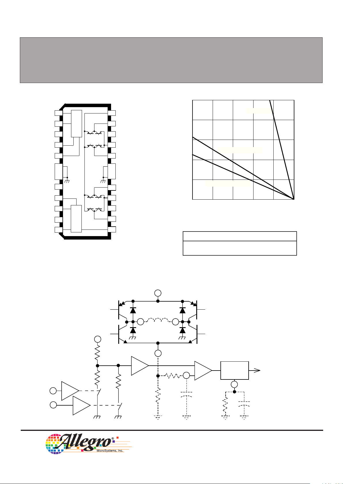
PWM CURRENT-CONTROL CIRCUITRY
V
BB
1
2
3
4
5
6
7
8
9
24
23
22
21
20
19
18
17
16
15
14
13
12
11
10
9
GROUND
GROUND
GROUND
GROUND
02
I
12
I
PHASE
2
V
REF 2
2
RC
V
CC
1
RC
V
REF 1
PHASE
1
11
I
2B
OUT
SENSE
2
2
E
2A
OUT
1A
OUT
1
E
SENSE
1
1B
OUT
01
I
LOAD SUPPLY
LOGIC SUPPLY
PWM 2
PWM 1
θ
1
θ
2
Dwg. PP-047
2
1
50 75 100 125 150
5
1
0
ALLOWABLE PACKAGE POWER DISSIPATION IN WATTS
TEMPERATURE IN °C
4
3
2
25
Dwg. GP-049A
R = 6.0°C/W
θJT
SUFFIX 'B', R = 40°C/W
θJA
SUFFIX 'LB', R = 55°C/W
θJA
TRUTH TABLE
PHASE OUT
A
OUT
B
HHL
LLH
V
REF
Dwg. EP-007-3
V
BB
SENSE
ONE
SHOT
SOURCE
DISABLE
RC
–
+
I
0
I
1
÷10
E
OUT
A
OUT
B
'B' PACKAGE,
CHANNEL 1
PIN NUMBERS
SHOWN.
R
C
R
S
R
T
C
C
C
T
24
60 kΩ
120 kΩ
42 kΩ
211232214
20
17
15
W
Copyright © 1994 Allegro MicroSystems, Inc.
Page 3

2919
DUAL FULL-BRIDGE
MOTOR DRIVER
ELECTRICAL CHARACTERISTICS at T
A
= +25°C, TJ ≤ 150°C, V
BB
= 45 V, VCC = 4.75 V to 5.25 V,
V
REF
= 5.0 V (unless otherwise noted).
(at trip point)
Limits
Characteristic Symbol Test Conditions Min. Typ. Max. Units
Output Drivers (OUTA or OUTB)
Motor Supply Range V
BB
Operating 10 — 45 V
Output Leakage Current I
CEX
V
OUT
= V
BB
— < 1.0 50 µA
V
OUT
= 0 — <-1.0 -50 µA
Output Sustaining Voltage V
CE(sus)
I
OUT
= ±750 mA, L = 3.0 mH 45 + V
F
——V
Output Saturation Voltage V
CE(SAT)
Sink Driver, I
OUT
= +500 mA — 0.4 0.6 V
Sink Driver, I
OUT
= +750 mA — 1.0 1.2 V
Source Driver, I
OUT
= -500 mA — 1.0 1.2 V
Source Driver, I
OUT
= -750 mA — 1.3 1.5 V
Clamp Diode Leakage Current I
R
VR = 45 V — < 1.0 50 µA
Clamp Diode Forward Voltage V
F
IF = 750 mA — 1.6 2.0 V
Driver Supply Current I
BB(ON)
Both Bridges ON, No Load — 20 25 mA
I
BB(OFF)
Both Bridges OFF — 5.0 10 mA
Control Logic
Input Voltage V
IN(1)
All inputs 2.4 — — V
V
IN(0)
All inputs — — 0.8 V
Input Current I
IN(1)
VIN = 2.4 V — <1.0 20 µA
V
IN
= 0.8 V — - 3.0 -200 µA
Reference Voltage Range V
REF
1.0 — 7.5 V
Current Limit Threshold V
REF/VSENSEI0
= I1 = 0.8 V, V
REF
= 1.0 V to 7.5 V 9.5 10 10.5 —
I
0
= 2.4 V, I1 = 0.8 V, 13.5 15 16.5 —
V
REF
= 1.5 V to 7.5 V
I
0
= 0.8 V, I1 = 2.4 V, 20.7 24.4 28.0 —
V
REF
= 1.5 V to 7.5 V
Thermal Shutdown Temperature T
J
— 170 — °C
Total Logic Supply Current I
CC(ON)
I0 = I1 = 0.8 V, No Load — 40 50 mA
I
CC(OFF)
I0 = I1 = 2.4 V, No Load — 10 12 mA
Total Reference Current I
REF1
+ I
REF2
V
REF1
= V
REF2
= 7.5 V, I0 = I1 = 2.4 V 140 185 250 µA
Page 4

2919
DUAL FULL-BRIDGE
MOTOR DRIVER
115 Northeast Cutoff, Box 15036
Worcester, Massachusetts 01615-0036 (508) 853-5000
APPLICATIONS INFORMATION
PWM CURRENT CONTROL
The A2919SB/SLB dual bridges are
designed to drive both windings of a bipolar
stepper motor. Output current is sensed and
controlled independently in each bridge by
an external sense resistor (RS), internal
comparator, and monostable multivibrator.
When the bridge is turned ON, current
increases in the motor winding and flows
through the external sense resistor until the
sense voltage (VS) reaches the level set at
the comparator’s input:
I
TRIP
= V
REF
/10 R
S
The comparator then triggers the
monostable, which turns OFF the source
driver of the bridge. The actual load current
peak will be slightly higher than the trip point
(especially for low-inductance loads) because of the internal logic and switching
delays. This delay (td) is typically 2 µs. After
turn-off, the motor current decays, circulating
through the ground-clamp diode and sink
transistor. The source driver’s OFF time
(and therefore the magnitude of the current
decrease) is determined by the monostable’s
external RC timing components, where
t
off
= RTCT within the range of 20 kΩ to
100 kΩ and 100 pF to 1000 pF.
When the source driver is re-enabled,
the winding current (the sense voltage) is
again allowed to rise to the comparator’s
threshold. This cycle repeats itself, maintaining the average motor winding current at the
desired level.
Loads with high distributed capacitances
may cause current spikes capable of tripping
the comparator, resulting in erroneous
current control. An external RCCC time delay
should be used to delay the action of the
comparator. Depending on load type, many
applications will not require these external
components (SENSE connected to E).
PWM OUTPUT CURRENT WAVE FORM
LOAD CURRENT PATHS
+
–
0
Dwg. WM-003-1A
V
PHASE
I
OUT
t
d
t
off
I
TRIP
Dwg. EP-006-1
R
S
BB
V
BRIDGE ON
SOURCE OFF
ALL OFF
Page 5

2919
DUAL FULL-BRIDGE
MOTOR DRIVER
LOGIC CONTROL OF OUTPUT CURRENT
Two logic level inputs (l0 and I1) allow digital selection
of the motor winding current at 100%, 67%, 41%, or 0% of
the maximum level per the table. The 0% output current
condition turns OFF all drivers in the bridge and can be
used as an OUTPUT ENABLE function.
CURRENT-CONTROL TRUTH TABLE
l
0
I
1
Output Current
LL V
REF
/10 RS = 100% I
TRIP
HLV
REF
/15 RS = 67% I
TRIP
LHV
REF
/24.4 RS = 41% I
TRIP
HH 0
These logic level inputs greatly enhance the implementation of µP-controlled drive formats.
During half-step operations, l0 and l
1
allow the µP to
control the motor at a constant torque between all positions in an eight-step sequence. This is accomplished by
digitally selecting 100% drive current when only one phase
is ON and 67% drive current when two phases are ON.
Logic highs on both l0 and l
1
turn OFF all drivers to allow
rapid current decay.
During quarter-step operation, I0 and I1 allow the µP to
control the motor position in a sixteen-step sequence.
This is accomplished by digitally selecting drive current as
shown in the table (for one quadrant of operation). Logic
highs on both I0 and I1 turn OFF all drivers to allow rapid
current decay.
The logic control inputs can also be used to select a
reduced current level (and reduced power dissipation) for
‘hold’ conditions and/or increased current (and available
torque) for start-up conditions.
QUARTER-STEPPING CURRENT CONTROL
Phase 1 Phase 2
Current Level Current Level
100% 0%
100% 41%
67% 67%
41% 100%
0% 100%
GENERAL
The PHASE input to each bridge determines the
direction motor winding current flows. An internally
generated deadtime (approximately 2 µs) prevents crossover currents that can occur when switching the PHASE
input.
All four drivers in the bridge output can be turned OFF
between steps (l0 = l1 ≥ 2.4 V) resulting in a fast current
decay through the internal output clamp and flyback
diodes. The fast current decay is desirable in half-step and
high-speed applications. The PHASE, l0, and I1 inputs
float high.
Varying the reference voltage (V
REF
) provides continuous control of the peak load current for micro-stepping
applications.
Thermal protection circuitry turns OFF all drivers when
the junction temperature reaches +170°C. It is only
intended to protect the device from failures due to excessive junction temperature and should not imply that output
short circuits are permitted. The output drivers are reenabled when the junction temperature cools to +145°C.
The A2919SB/SLB output drivers are optimized for
low output saturation voltages—less than 1.8 V total
(source plus sink) at 500 mA. Under normal operating
conditions, when combined with the excellent thermal
properties of the batwing package design, this allows
continuous operation of both bridges simultaneously at
500 mA.
Page 6

2919
DUAL FULL-BRIDGE
MOTOR DRIVER
115 Northeast Cutoff, Box 15036
Worcester, Massachusetts 01615-0036 (508) 853-5000
TYPICAL APPLICATION
FROM
µP
V
REF
Dwg. EP-008B
V
BB
FROM
µP
1
2
3
4
5
6
7
8
9
24
23
22
21
20
19
18
17
16
15
14
1312
11
10
9
θ
2
θ
1
V
CC
PWM 2
PWM 1
2
V
BB
1
V
REF
+5 V
STEPPER
MOTOR
R
S
R
S
R
C
R
C
R
T
R
T
C
T
C
T
C
C
C
C
+
Page 7

2919
DUAL FULL-BRIDGE
MOTOR DRIVER
0.014
0.008
0.300
BSC
Dwg. MA-001-25A in
0.430
MAX
24
16
12
0.280
0.240
0.210
MAX
0.070
0.045
0.015
MIN
0.022
0.014
0.100
BSC
0.005
MIN
0.150
0.115
13
1.280
1.230
NOTE 1
7
0.355
0.204
7.62
BSC
Dwg. MA-001-25A mm
10.92
MAX
24
1
12
7.11
6.10
5.33
MAX
1.77
1.15
0.39
MIN
0.558
0.356
2.54
BSC
0.13
MIN
3.81
2.93
13
32.51
31.24
NOTE 1
67
A2919SB
Dimensions in Inches
(controlling dimensions)
Dimensions in Millimeters
(for reference only)
NOTES: 1. Webbed lead frame. Leads 6, 7, 18, and 19 are internally one piece.
2. Lead thickness is measured at seating plane or below.
3. Lead spacing tolerance is non-cumulative.
4. Exact body and lead configuration at vendor’s option within limits shown.
Page 8

2919
DUAL FULL-BRIDGE
MOTOR DRIVER
115 Northeast Cutoff, Box 15036
Worcester, Massachusetts 01615-0036 (508) 853-5000
A2919SLB
Dimensions in Inches
(for reference only)
Dimensions in Millimeters
(controlling dimensions)
NOTES: 1. Webbed lead frame. Leads 6, 7, 18, and 19 are internally
one piece.
2. Lead spacing tolerance is non-cumulative.
3. Exact body and lead configuration at vendor’s option
within limits shown.
0° TO 8
°
1 2
3
0.2992
0.2914
0.6141
0.5985
0.491
0.394
0.020
0.013
0.0926
0.1043
0.0040
MIN
.
0.0125
0.0091
Dwg. MA-008-25 in
0.050
BSC
24 13
NOTE 1
NOTE 3
0.050
0.016
0° TO 8
°
1 2
3
7.60
7.40
15.60
15.20
10.65
10.00
0.51
0.33
2.65
2.35
0.10 MIN
.
0.32
0.23
Dwg. MA-008-25A mm
1.27
BSC
24 13
NOTE 1
NOTE 3
1.27
0.40
Allegro MicroSystems, Inc. reserves the right to make, from time to time, such
departures from the detail specifications as may be required to permit improvements
in the design of its products.
The information included herein is believed to be accurate and reliable.
However, Allegro MicroSystems, Inc. assumes no responsibility for its use; nor for
any infringements of patents or other rights of third parties which may result from its
use.
 Loading...